Document Outline
- Cover Sheet
- Am29DL32xD
- Distinctive Characteristics
- General Description
- Product Selector Guide
- Block Diagram
- Connection Diagrams
- Pin Description
- Logic Symbol
- Ordering Information
- Device Bus Operations
- Common Flash Memory Interface (CFI)
- Command Definitions
- Write Operation Status
- Absolute Maximum Ratings
- DC Characteristics
- Test Conditions
- AC Characteristics
- Erase And Programming Performance
- Latchup Characteristics
- TSOP And SO Pin Capacitance
- Data Retention
- Physical Dimensions
- Revision Summary
- Revision B (October 1998)
- Revision B+1 (October 1998)
- Revision C (January 1999)
- Revision C+1 (January 1999)
- Revision C+2 (March 17, 1999)
- Revision C+3 (June 14, 1999)
- Revision C+4 (July 2, 1999)
- Revision C+5 (September 27, 1999)
- Revision D (December 17, 1999)
- Revision D+1 (June 21, 2000)
- Revision D+2 (August 3, 2000)
- Revision D+3 (October 6, 2000)
- Revision D+4 (April 27, 2001)
- Revision D+5 (May 8, 2001)
- Revision D+6 (June 10, 2003)

-XO\
7KH IROORZLQJ GRFXPHQW VSHFLILHV 6SDQVLRQ PHPRU\ SURGXFWV WKDW DUH QRZ RIIHUHG E\ ERWK $GYDQFHG
0LFUR 'HYLFHV DQG )XMLWVX $OWKRXJK WKH GRFXPHQW LV PDUNHG ZLWK WKH QDPH RI WKH FRPSDQ\ WKDW RULJ
LQDOO\ GHYHORSHG WKH VSHFLILFDWLRQ WKHVH SURGXFWV ZLOO EH RIIHUHG WR FXVWRPHUV RI ERWK $0' DQG
)XMLWVX
Continuity of Specifications
7KHUH LV QR FKDQJH WR WKLV GDWDVKHHW DV D UHVXOW RI RIIHULQJ WKH GHYLFH DV D 6SDQVLRQ SURGXFW $Q\
FKDQJHV WKDW KDYH EHHQ PDGH DUH WKH UHVXOW RI QRUPDO GDWDVKHHW LPSURYHPHQW DQG DUH QRWHG LQ WKH
GRFXPHQW UHYLVLRQ VXPPDU\ ZKHUH VXSSRUWHG )XWXUH URXWLQH UHYLVLRQV ZLOO RFFXU ZKHQ DSSURSULDWH
DQG FKDQJHV ZLOO EH QRWHG LQ D UHYLVLRQ VXPPDU\
Continuity of Ordering Part Numbers
$0' DQG )XMLWVX FRQWLQXH WR VXSSRUW H[LVWLQJ SDUW QXPEHUV EHJLQQLQJ ZLWK ≥$P¥ DQG ≥0%0¥ 7R RUGHU
WKHVH SURGXFWV SOHDVH XVH RQO\ WKH 2UGHULQJ 3DUW 1XPEHUV OLVWHG LQ WKLV GRFXPHQW
For More Information
3OHDVH FRQWDFW \RXU ORFDO $0' RU )XMLWVX VDOHV RIILFH IRU DGGLWLRQDO LQIRUPDWLRQ DERXW 6SDQVLRQ
PHPRU\ VROXWLRQV
Am29DL322D/323D/324D
Data Sheet
Publication Number 21534 Revision
D
Amendment +6 Issue
Date
June 10, 2003

Publication# 21534
Rev: D Amendment/+6
Issue Date: June 10, 2003
Refer to AMD's Website (www.amd.com) for the latest information.
Am29DL322D/323D/324D
32 Megabit (4 M x 8-Bit/2 M x 16-Bit)
CMOS 3.0 Volt-only, Simultaneous Operation Flash Memory
DISTINCTIVE CHARACTERISTICS
ARCHITECTURAL ADVANTAGES
Simultaneous Read/Write operations
-- Data can be continuously read from one bank while
executing erase/program functions in other bank.
-- Zero latency between read and write operations
Multiple bank architectures
-- Three devices available with different bank sizes
(refer to Table 3)
SecSi
(Secured Silicon) Sector
-- Current version of device has 64 Kbytes; future
versions will have 256 bytes
-- Factory locked and identifiable: 16 bytes available for
secure, random factory Electronic Serial Number;
verifiable as factory locked through autoselect
function. ExpressFlash option allows entire sector to
be available for factory-secured data
-- Customer lockable: Can be read, programmed, or
erased just like other sectors. Once locked, data
cannot be changed
Zero Power Operation
-- Sophisticated power management circuits reduce
power consumed during inactive periods to nearly
zero.
Package options
-- 63-ball FBGA
-- 48-pin TSOP
Top or bottom boot block
Manufactured on 0.23 µm process technology
Compatible with JEDEC standards
-- Pinout and software compatible with
single-power-supply flash standard
PERFORMANCE CHARACTERISTICS
High performance
-- Access time as fast 70 ns
-- Program time: 7 µs/word typical utilizing Accelerate
function
Ultra low power consumption (typical values)
-- 2 mA active read current at 1 MHz
-- 10 mA active read current at 5 MHz
-- 200 nA in standby or automatic sleep mode
Minimum 1 million write cycles guaranteed per
sector
20 year data retention at 125
∞
C
-- Reliable operation for the life of the system
SOFTWARE FEATURES
Data Management Software (DMS)
-- AMD-supplied software manages data programming,
enabling EEPROM emulation
-- Eases historical sector erase flash limitations
Supports Common Flash Memory Interface (CFI)
Erase Suspend/Erase Resume
-- Suspends erase operations to allow programming in
same bank
Data# Polling and Toggle Bits
-- Provides a software method of detecting the status of
program or erase cycles
Unlock Bypass Program command
-- Reduces overall programming time when issuing
multiple program command sequences
HARDWARE FEATURES
Any combination of sectors can be erased
Ready/Busy# output (RY/BY#)
-- Hardware method for detecting program or erase
cycle completion
Hardware reset pin (RESET#)
-- Hardware method of resetting the internal state
machine to the read mode
WP#/ACC input pin
-- Write protect (WP#) function allows protection of two
outermost boot sectors, regardless of sector protect
status
-- Acceleration (ACC) function accelerates program
timing
Sector protection
-- Hardware method of locking a sector, either
in-system or using programming equipment, to
prevent any program or erase operation within that
sector
-- Temporary Sector Unprotect allows changing data in
protected sectors in-system
2
Am29DL322D/323D/324D
June 10, 2003
GENERAL DESCRIPTION
The Am29DL322D/323D/324D family consists of
32 megabit, 3.0 volt-only flash memory devices, orga-
nized as 2,097,152 words of 16 bits each or 4,194,304
bytes of 8 bits each. Word mode data appears on
DQ0≠DQ15; byte mode data appears on DQ0≠DQ7.
The device is designed to be programmed in-system
with the standard 3.0 volt V
CC
supply, and can also be
programmed in standard EPROM programmers.
The devices are available with an access time of 70,
90 or 120 ns. The devices are offered in 48-pin TSOP
and 63-ball FBGA packages. Standard control
pins--chip enable (CE#), write enable (WE#), and out-
put enable (OE#)--control normal read and write oper-
ations, and avoid bus contention issues.
The devices requires only a single 3.0 volt power
supply for both read and write functions. Internally
generated and regulated voltages are provided for the
program and erase operations.
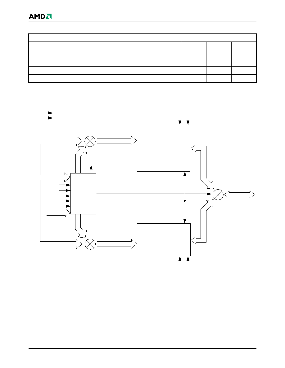
Simultaneous Read/Write Operations with
Zero Latency
The Simultaneous Read/Write architecture provides
simultaneous operation by dividing the memory
space into two banks. The device can improve overall
system performance by allowing a host system to pro-
gram or erase in one bank, then immediately and si-
multaneously read from the other bank, with zero
latency. This releases the system from waiting for the
completion of program or erase operations.
The Am29DL32xD device family uses multiple bank
architectures to provide flexibility for different applica-
tions. Three devices are available with the following
bank sizes:
Am29DL322D/323D/324D Features
The
SecSi
(Secured Silicon) Sector
is an extra sector
capable of being permanently locked by AMD or cus-
tomers. The SecSi Indicator Bit (DQ7) is perma-
nently set to a 1 if the part is factory locked, and set
to a 0 if customer lockable. This way, customer lock-
able parts can never be used to replace a factory
locked part. Current version of device has 64
Kbytes; future versions will have only 256 bytes.
This should be considered during system design.
Factory locked parts provide several options. The
SecSi Sector may store a secure, random 16 byte
ESN (Electronic Serial Number), customer code (pro-
grammed through AMD's ExpressFlash service), or
both. Customer Lockable parts may utilize the SecSi
Sector as bonus space, reading and writing like any
other flash sector, or may permanently lock their own
code there.
DMS (Data Management Software) allows systems
to easily take advantage of the advanced architecture
of the simultaneous read/write product line by allowing
removal of EEPROM devices. DMS will also allow the
system software to be simplified, as it will perform all
functions necessary to modify data in file structures,
as opposed to single-byte modifications. To write or
update a particular piece of data (a phone number or
configuration data, for example), the user only needs
to state which piece of data is to be updated, and
where the updated data is located in the system. This
is an advantage compared to systems where
user-written software must keep track of the old data
location, status, logical to physical translation of the
data onto the Flash memory device (or memory de-
vices), and more. Using DMS, user-written software
does not need to interface with the Flash memory di-
rectly. Instead, the user's software accesses the Flash
memory by calling one of only six functions. AMD pro-
vides this software to simplify system design and soft-
ware integration efforts.
The device offers complete compatibility with the
JEDEC single-power-supply Flash command set
standard. Commands are written to the command
register using standard microprocessor write timings.
Reading data out of the device is similar to reading
from other Flash or EPROM devices.
The host system can detect whether a program or
erase operation is complete by using the device sta-
tus bits: RY/BY# pin, DQ7 (Data# Polling) and
DQ6/DQ2 (toggle bits). After a program or erase cycle
has been completed, the device automatically returns
to the read mode.
The sector erase architecture allows memory sec-
tors to be erased and reprogrammed without affecting
the data contents of other sectors. The device is fully
erased when shipped from the factory.
Hardware data protection measures include a low
V
CC
detector that automatically inhibits write opera-
tions during power transitions. The hardware sector
protection feature disables both program and erase
operations in any combination of the sectors of mem-
ory. This can be achieved in-system or via program-
ming equipment.
The device offers two power-saving features. When
addresses have been stable for a specified amount of
time, the device enters the automatic sleep mode.
The system can also place the device into the
standby mode. Power consumption is greatly re-
duced in both modes.
Device
Bank 1
Bank 2
DL322
4
28
DL323
8
24
DL324
16
16

June 10, 2003
Am29DL322D/323D/324D
3
TABLE OF CONTENTS
Product Selector Guide . . . . . . . . . . . . . . . . . . . . . 4
Block Diagram . . . . . . . . . . . . . . . . . . . . . . . . . . . . 4
Connection Diagrams . . . . . . . . . . . . . . . . . . . . . . . 5
Special Handling Instructions for FBGA Package ..........................6
Pin Description . . . . . . . . . . . . . . . . . . . . . . . . . . . . 6
Logic Symbol . . . . . . . . . . . . . . . . . . . . . . . . . . . . . 6
Ordering Information . . . . . . . . . . . . . . . . . . . . . . . 7
Device Bus Operations . . . . . . . . . . . . . . . . . . . . . . 8
Word/Byte Configuration ................................................................ 8
Requirements for Reading Array Data ...........................................8
Writing Commands/Command Sequences ....................................9
Simultaneous Read/Write Operations
with Zero Latency ...........................................................................9
Standby Mode ................................................................................ 9
Automatic Sleep Mode ...................................................................9
RESET#: Hardware Reset Pin .....................................................10
Output Disable Mode ...................................................................10
Autoselect Mode .......................................................................... 15
Sector/Sector Block Protection and Unprotection ........................ 16
Write Protect (WP#) .....................................................................17
Temporary Sector Unprotect ........................................................17
Figure 1. Temporary Sector Unprotect Operation................................. 17
Figure 2. In-System Sector Protection/
Sector Unprotection Algorithms ............................................................ 18
SecSi (Secured Silicon) Sector
Flash Memory Region ..................................................................19
Hardware Data Protection ............................................................20
Common Flash Memory Interface (CFI) . . . . . . . 20
Command Definitions . . . . . . . . . . . . . . . . . . . . . . 22
Reading Array Data ......................................................................22
Reset Command ..........................................................................23
Autoselect Command Sequence ..................................................23
Enter SecSi Sector/Exit SecSi Sector
Command Sequence ...................................................................23
Byte/Word Program Command Sequence ...................................23
Figure 3. Program Operation ................................................................ 24
Chip Erase Command Sequence .................................................24
Sector Erase Command Sequence ..............................................25
Erase Suspend/Erase Resume Commands ................................25
Figure 4. Erase Operation..................................................................... 26
Write Operation Status . . . . . . . . . . . . . . . . . . . . . 28
DQ7: Data# Polling ......................................................................28
Figure 5. Data# Polling Algorithm ......................................................... 28
RY/BY#: Ready/Busy# ................................................................. 29
DQ6: Toggle Bit I .......................................................................... 29
Figure 6. Toggle Bit Algorithm .............................................................. 29
DQ2: Toggle Bit II ......................................................................... 30
Reading Toggle Bits DQ6/DQ2 .................................................... 30
DQ5: Exceeded Timing Limits ...................................................... 30
DQ3: Sector Erase Timer ............................................................. 30
Absolute Maximum Ratings . . . . . . . . . . . . . . . . 32
Figure 7. Maximum Negative Overshoot Waveform............................. 32
Figure 8. Maximum Positive Overshoot Waveform .............................. 32
DC Characteristics . . . . . . . . . . . . . . . . . . . . . . . . 33
Figure 9. I
CC1
Current vs. Time (Showing Active and
Automatic Sleep Currents).................................................................... 34
Figure 10. Typical I
CC1
vs. Frequency................................................... 34
Test Conditions . . . . . . . . . . . . . . . . . . . . . . . . . . 35
Figure 11. Test Setup .......................................................................... 35
Figure 12. Input Waveforms and Measurement Levels ........................ 35
AC Characteristics . . . . . . . . . . . . . . . . . . . . . . . . 36
Figure 13. Read Operation Timings...................................................... 36
Figure 14. Reset Timings...................................................................... 37
Word/Byte Configuration (BYTE#) ............................................... 38
Figure 15. BYTE# Timings for Read Operations .................................. 38
Figure 16. BYTE# Timings for Write Operations .................................. 38
Erase and Program Operations ................................................... 39
Figure 17. Program Operation Timings ................................................ 40
Figure 18. Accelerated Program Timing Diagram ................................ 40
Figure 19. Chip/Sector Erase Operation Timings ................................. 41
Figure 20. Back-to-back Read/Write Cycle Timings ............................. 42
Figure 21. Data# Polling Timings (During Embedded Algorithms) ....... 42
Figure 22. Toggle Bit Timings (During Embedded Algorithms) ............ 43
Figure 23. DQ2 vs. DQ6 ....................................................................... 43
Temporary Sector Unprotect ........................................................ 44
Figure 24. Temporary Sector Unprotect Timing Diagram..................... 44
Figure 25. Sector/Sector Block Protect and Unprotect Timing Diagram 45
Alternate CE# Controlled Erase and Program Operations ........... 46
Figure 26. Alternate CE# Controlled Write (Erase/Program)
Operation Timings ................................................................................ 47
Erase And Programming Performance . . . . . . . 48
Latchup Characteristics . . . . . . . . . . . . . . . . . . . . 48
TSOP And SO Pin Capacitance . . . . . . . . . . . . . . 48
Data Retention. . . . . . . . . . . . . . . . . . . . . . . . . . . . 48
Physical Dimensions . . . . . . . . . . . . . . . . . . . . . . 49
FBD063--63-ball Fine-Pitch Ball Grid Array (FBGA) 8 x 14 mm . 49
TS 048--48-Pin Standard TSOP ................................................. 50
Revision Summary . . . . . . . . . . . . . . . . . . . . . . . . 51
4
Am29DL322D/323D/324D
June 10, 2003
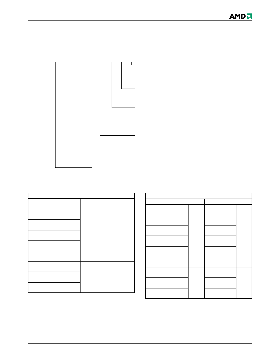
PRODUCT SELECTOR GUIDE
BLOCK DIAGRAM
Part Number
Am29DL322D/323D/324D
Speed Option
Regulated Voltage Range: V
CC
= 3.0≠3.6 V
70R
Standard Voltage Range: V
CC
= 2.7≠3.6 V
90
120
Max Access Time (ns)
70
90
120
CE# Access (ns)
70
90
120
OE# Access (ns)
30
40
50
V
CC
V
SS
Upper Bank Address
A20≠A0
RESET#
WE#
CE#
BYTE#
DQ15≠DQ0
WP#/ACC
STATE
CONTROL
&
COMMAND
REGISTER
RY/BY#
Upper Bank
X-Decoder
Y-Decoder
Latches and Control Logic
OE#
BYTE#
DQ15≠DQ0
Lower Bank
Y-Decoder
X-Decoder
Latches and
Control Logic
Lower Bank Address
OE#
BYTE#
Status
Control
A20≠A0
A20≠A0
A20≠A0
A20≠A0
DQ15≠DQ0
DQ15≠DQ0
June 10, 2003
Am29DL322D/323D/324D
5
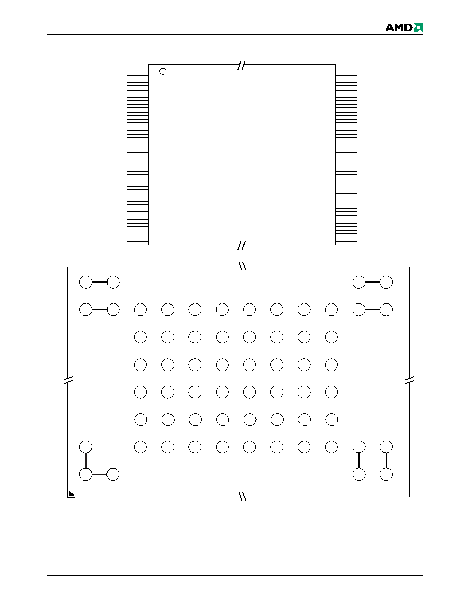
CONNECTION DIAGRAMS
1
16
2
3
4
5
6
7
8
17
18
19
20
21
22
23
24
9
10
11
12
13
14
15
48
33
47
46
45
44
43
42
41
40
39
38
37
36
35
34
25
32
31
30
29
28
27
26
A15
A18
A14
A13
A12
A11
A10
A9
A8
A19
A20
WE#
RESET#
NC
WP#/ACC
RY/BY#
A1
A17
A7
A6
A5
A4
A3
A2
A16
DQ2
BYTE#
V
SS
DQ15/A-1
DQ7
DQ14
DQ6
DQ13
DQ9
DQ1
DQ8
DQ0
OE#
V
SS
CE#
A0
DQ5
DQ12
DQ4
V
CC
DQ11
DQ3
DQ10
48-Pin Standard TSOP
C2
D2
E2
F2
G2
H2
J2
K2
C3
D3
E3
F3
G3
H3
J3
K3
C4
D4
E4
F4
G4
H4
J4
K4
C5
D5
E5
F5
G5
H5
J5
K5
C6
D6
E6
F6
G6
H6
J6
K6
C7
D7
A7
B7
A8
B8
A1
B1
A2
E7
F7
G7
H7
J7
K7
L7
L8
M7
M8
L1
L2
M1
M2
NC*
NC*
NC*
NC*
NC*
NC*
NC*
NC*
NC*
NC*
NC*
NC
NC
NC
NC
DQ15/A-1
V
SS
BYTE#
A16
A15
A14
A12
A13
DQ13
DQ6
DQ14
DQ7
A11
A10
A8
A9
V
CC
DQ4
DQ12
DQ5
A19
NC
RESET#
WE#
DQ11
DQ3
DQ10
DQ2
A20
A18
WP#/ACC
RY/BY#
DQ9
DQ1
DQ8
DQ0
A5
A6
A17
A7
OE#
V
SS
CE#
A0
A1
A2
A4
A3
* Balls are shorted together via the substrate but not connected to the die.
63-Ball FBGA
Top View, Balls Facing
Down
6
Am29DL322D/323D/324D
June 10, 2003
Special Handling Instructions for FBGA
Package
Special handling is required for Flash Memory products
in FBGA packages.
Flash memory devices in FBGA packages may be
damaged if exposed to ultrasonic cleaning methods.
The package and/or data integrity may be compromised
if the package body is exposed to temperatures above
150
∞
C for prolonged periods of time.
PIN DESCRIPTION
A0≠A20
= 21 Addresses
DQ0≠DQ14 = 15 Data Inputs/Outputs
DQ15/A-1
= DQ15 (Data Input/Output, word
mode), A-1 (LSB Address Input, byte
mode)
CE#
= Chip Enable
OE#
= Output Enable
WE#
= Write Enable
WP#/ACC
= Hardware Write Protect/
Acceleration Pin
RESET#
= Hardware Reset Pin, Active Low
BYTE#
= Selects 8-bit or 16-bit mode
RY/BY#
= Ready/Busy Output
V
CC
= 3.0 volt-only single power supply
(see Product Selector Guide for speed
options and voltage supply toler-
ances)
V
SS
= Device Ground
NC
= Pin Not Connected Internally
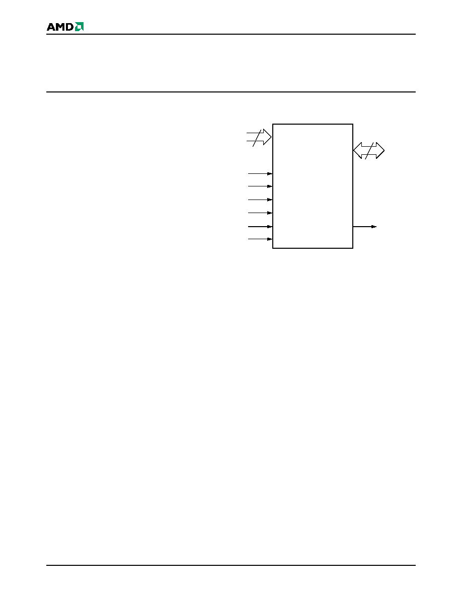
LOGIC SYMBOL
21
16 or 8
DQ0≠DQ15
(A-1)
A0≠A20
CE#
OE#
WE#
RESET#
BYTE#
RY/BY#
WP#/ACC
June 10, 2003
Am29DL322D/323D/324D
7
ORDERING INFORMATION
Standard Products
AMD standard products are available in several packages and operating ranges. The order number (Valid Combination) is
formed by a combination of the following:
Valid Combinations
Valid Combinations list configurations planned to be supported in
volume for this device. Consult the local AMD sales office to con-
firm availability of specific valid combinations and to check on
newly released combinations.
Am29DL322D/323D/324D
T
70R
E
I
OPTIONAL PROCESSING
Blank =
Standard Processing
N
=
16-byte ESN devices
(Contact an AMD representative for more information)
TEMPERATURE RANGE
I =
Industrial
(≠40
∞
C to +85
∞
C)
E =
Extended
(≠55
∞
C to +125
∞
C)
PACKAGE TYPE
E
=
48-Pin Thin Small Outline Package
(TSOP) Standard Pinout (TS 048)
WD
=
63-Ball Fine-Pitch Ball Grid Array (FBGA)
0.80 mm pitch, 8 x 14 mm package (FBD063)
SPEED OPTION
See Product Selector Guide and Valid Combinations
BOOT CODE SECTOR ARCHITECTURE
T
=
Top sector
B
=
Bottom sector
DEVICE NUMBER/DESCRIPTION
Am29DL322D/323D/324D
32 Megabit (4 M x 8-Bit/2 M x 16-Bit) CMOS Flash Memory
3.0 Volt-only Read, Program, and Erase
Valid Combinations for TSOP Packages
AM29DL322DT70R,
AM29DL322DB70R
EI, EIN
AM29DL323DT70R,
AM29DL323DB70R
AM29DL324DT70R,
AM29DL324DB70R
AM29DL322DT90,
AM29DL322DB90
AM29DL323DT90,
AM29DL323DB90
AM29DL324DT90,
AM29DL324DB90
AM29DL322DT120,
AM29DL322DB120
EI, EIN, EE, EEN
AM29DL323DT120,
AM29DL323DB120
AM29DL324DT120,
AM29DL324DB120
Valid Combinations for FBGA Packages
Order Number
Package Marking
AM29DL322DT70R,
AM29DL322DB70R
WDI,
WDIN
D322DT70R,
D322DB70R
I
AM29DL323DT70R,
AM29DL323DB70R
D323DT70R,
D323DB70R
AM29DL324DT70R,
AM29DL324DB70R
D324DT70R,
D324DB70R
AM29DL322DT90,
AM29DL322DB90
D322DT90V,
D322DB90V
AM29DL323DT90,
AM29DL323DB90
D323DT90V,
D323DB90V
AM29DL324DT90,
AM29DL324DB90
D324DT90V,
D324DB90V
AM29DL322DT120,
AM29DL322DB120
WDI,
WDIN,
WDE,
WDEN
D322DT12V,
D322DB12V
I, E
AM29DL323DT120,
AM29DL323DB120
D323DT12V,
D323DB12V
AM29DL324DT120,
AM29DL324DB120
D324DT12V,
D324DB12V
8
Am29DL322D/323D/324D
June 10, 2003
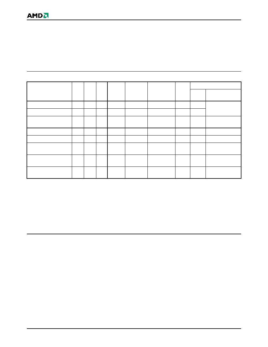
DEVICE BUS OPERATIONS
This section describes the requirements and use of
the device bus operations, which are initiated through
the internal command register. The command register
itself does not occupy any addressable memory loca-
tion. The register is a latch used to store the com-
mands, along with the address and data information
needed to execute the command. The contents of the
register serve as inputs to the internal state machine.
The state machine outputs dictate the function of the
device. Table 1 lists the device bus operations, the in-
puts and control levels they require, and the resulting
output. The following subsections describe each of
these operations in further detail.
Table 1. Device Bus Operations
Legend: L = Logic Low = V
IL
, H = Logic High = V
IH
, V
ID
= 8.5≠12.5
V, V
HH
= 9.0 ± 0.5 V, X = Don't Care, SA = Sector Address,
A
IN
= Address In, D
IN
= Data In, D
OUT
= Data Out
Notes:
1. Addresses are A20:A0 in word mode (BYTE# = V
IH
), A20:A-1 in byte mode (BYTE# = V
IL
).
2. The sector protect and sector unprotect functions may also be implemented via programming equipment. See the "Sector/Sector
Block Protection and Unprotection" section.
3. If WP#/ACC = V
IL
, the two outermost boot sectors remain protected. If WP#/ACC = V
IH
, the two outermost boot sector
protection depends on whether they were last protected or unprotected using the method described in "Sector/Sector Block
Protection and Unprotection". If WP#/ACC = V
HH
, all sectors will be unprotected.
Word/Byte Configuration
The BYTE# pin controls whether the device data I/O
pins operate in the byte or word configuration. If the
BYTE# pin is set at logic `1', the device is in word con-
figuration, DQ0≠DQ15 are active and controlled by
CE# and OE#.
If the BYTE# pin is set at logic `0', the device is in byte
configuration, and only data I/O pins DQ0≠DQ7 are
active and controlled by CE# and OE#. The data I/O
pins DQ8≠DQ14 are tri-stated, and the DQ15 pin is
used as an input for the LSB (A-1) address function.
Requirements for Reading Array Data
To read array data from the outputs, the system must
drive the CE# and OE# pins to V
IL
. CE# is the power
control and selects the device. OE# is the output con-
trol and gates array data to the output pins. WE#
should remain at V
IH
. The BYTE# pin determines
whether the device outputs array data in words or
bytes.
The internal state machine is set for reading array data
upon device power-up, or after a hardware reset. This
ensures that no spurious alteration of the memory
content occurs during the power transition. No com-
mand is necessary in this mode to obtain array data.
Standard microprocessor read cycles that assert valid
Operation
CE#
OE#
WE# RESET#
WP#/ACC
Addresses
(Note 2)
DQ0≠
DQ7
DQ8≠DQ15
BYTE#
= V
IH
BYTE#
= V
IL
Read
L
L
H
H
L/H
A
IN
D
OUT
D
OUT
DQ8≠DQ14 =
High-Z, DQ15 = A-1
Write
L
H
L
H
(Note 3)
A
IN
D
IN
D
IN
Standby
V
CC
±
0.3 V
X
X
V
CC
±
0.3 V
H
X
High-Z
High-Z
High-Z
Output Disable
L
H
H
H
L/H
X
High-Z
High-Z
High-Z
Reset
X
X
X
L
L/H
X
High-Z
High-Z
High-Z
Sector Protect (Note 2)
L
H
L
V
ID
L/H
SA, A6 = L,
A1 = H, A0 = L
D
IN
X
X
Sector Unprotect (Note 2)
L
H
L
V
ID
(Note 3)
SA, A6 = H,
A1 = H, A0 = L
D
IN
X
X
Temporary Sector
Unprotect
X
X
X
V
ID
(Note 3)
A
IN
D
IN
D
IN
High-Z

June 10, 2003
Am29DL322D/323D/324D
9
addresses on the device address inputs produce valid
data on the device data outputs. Each bank remains
enabled for read access until the command register
contents are altered.
See "Requirements for Reading Array Data" for more
information. Refer to the AC Read-Only Operations
table for timing specifications and to Figure 13 for the
timing diagram. I
CC1
in the DC Characteristics table
represents the active current specification for reading
array data.
Writing Commands/Command Sequences
To write a command or command sequence (which in-
cludes programming data to the device and erasing
sectors of memory), the system must drive WE# and
CE# to V
IL
, and OE# to V
IH
.
For program operations, the BYTE# pin determines
whether the device accepts program data in bytes or
words. Refer to "Word/Byte Configuration" for more in-
formation.
The device features an Unlock Bypass mode to facil-
itate faster programming. Once a bank enters the Un-
lock Bypass mode, only two write cycles are required
to program a word or byte, instead of four. The
"Word/Byte Configuration" section has details on pro-
gramming data to the device using both standard and
Unlock Bypass command sequences.
An erase operation can erase one sector, multiple
sectors, or the entire device. Tables 3≠6 indicate the
address space that each sector occupies. The device
address space is divided into two banks: Bank 1 con-
tains the boot/parameter sectors, and Bank 2 contains
the larger, code sectors of uniform size. A "bank ad-
dress" is the address bits required to uniquely select a
bank. Similarly, a "sector address" is the address bits
required to uniquely select a sector.
I
CC2
in the DC Characteristics table represents the ac-
tive current specification for the write mode. The AC
Characteristics section contains timing specification
tables and timing diagrams for write operations.
Accelerated Program Operation
The device offers accelerated program operations
through the ACC function. This is one of two functions
provided by the WP#/ACC pin. This function is prima-
rily intended to allow faster manufacturing throughput
at the factory.
If the system asserts V
HH
on this pin, the device auto-
matically enters the aforementioned Unlock Bypass
mode, temporarily unprotects any protected sectors,
and uses the higher voltage on the pin to reduce the
time required for program operations. The system
would use a two-cycle program command sequence
as required by the Unlock Bypass mode. Removing
V
HH
from the WP#/ACC pin returns the device to nor-
mal operation. Note that the WP#/ACC pin must not
be at V
HH
for operations other than accelerated pro-
gramming, or device damage may result. In addition,
the WP#/ACC pin must not be left floating or uncon-
nected; inconsistent behavior of the device may result.
Autoselect Functions
If the system writes the autoselect command se-
quence, the device enters the autoselect mode. The
system can then read autoselect codes from the inter-
nal register (which is separate from the memory array)
on DQ7≠DQ0. Standard read cycle timings apply in
this mode. Refer to the Autoselect Mode and Autose-
lect Command Sequence sections for more informa-
tion.
Simultaneous Read/Write Operations
with Zero Latency
This device is capable of reading data from one bank
of memory while programming or erasing in the other
bank of memory. An erase operation may also be sus-
pended to read from or program to another location
within the same bank (except the sector being
erased). Figure 20 shows how read and write cycles
may be initiated for simultaneous operation with zero
latency. I
CC6
and I
CC7
in the DC Characteristics table
represent the current specifications for read-while-pro-
gram and read-while-erase, respectively.
Standby Mode
When the system is not reading or writing to the de-
vice, it can place the device in the standby mode. In
this mode, current consumption is greatly reduced,
and the outputs are placed in the high impedance
state, independent of the OE# input.
The device enters the CMOS standby mode when the
CE# and RESET# pins are both held at V
CC
± 0.3 V.
(Note that this is a more restricted voltage range than
V
IH
.) If CE# and RESET# are held at V
IH
, but not within
V
CC
± 0.3 V, the device will be in the standby mode,
but the standby current will be greater. The device re-
quires standard access time (t
CE
) for read access
when the device is in either of these standby modes,
before it is ready to read data.
If the device is deselected during erasure or program-
ming, the device draws active current until the
operation is completed.
I
CC3
in the DC Characteristics table represents the
standby current specification.
Automatic Sleep Mode
The automatic sleep mode minimizes Flash device en-
ergy consumption. The device automatically enables
10
Am29DL322D/323D/324D
June 10, 2003
this mode when addresses remain stable for t
ACC
+
30 ns. The automatic sleep mode is independent of
the CE#, WE#, and OE# control signals. Standard ad-
dress access timings provide new data when ad-
dresses are changed. While in sleep mode, output
data is latched and always available to the system.
I
CC5
in the DC Characteristics table represents the
automatic sleep mode current specification.
RESET#: Hardware Reset Pin
The RESET# pin provides a hardware method of re-
setting the device to reading array data. When the RE-
SET# pin is driven low for at least a period of t
RP
, the
device immediately terminates any operation in
progress, tristates all output pins, and ignores all
read/write commands for the duration of the RESET#
pulse. The device also resets the internal state ma-
chine to reading array data. The operation that was in-
terrupted should be reinitiated once the device is
ready to accept another command sequence, to en-
sure data integrity.
Current is reduced for the duration of the RESET#
pulse. When RESET# is held at V
SS
±0.3 V, the device
draws CMOS standby current (I
CC4
). If RESET# is held
at V
IL
but not within V
SS
±0.3 V, the standby current will
be greater.
The RESET# pin may be tied to the system reset cir-
cuitry. A system reset would thus also reset the Flash
memory, enabling the system to read the boot-up firm-
ware from the Flash memory.
If RESET# is asserted during a program or erase op-
eration, the RY/BY# pin remains a "0" (busy) until the
internal reset operation is complete, which requires a
time of t
READY
(during Embedded Algorithms). The
system can thus monitor RY/BY# to determine
whether the reset operation is complete. If RESET# is
asserted when a program or erase operation is not ex-
ecuting (RY/BY# pin is "1"), the reset operation is com-
pleted within a time of t
READY
(not during Embedded
Algorithms). The system can read data t
RH
after the
RESET# pin returns to V
IH
.
I
CC4
in the DC Characteristics table represents the
reset current. Also refer to AC Characteristics tables
for RESET# timing parameters and to Figure 14 for
the timing diagram.
Output Disable Mode
When the OE# input is at V
IH
, output from the device is
disabled. The output pins are placed in the high
impedance state.
Table 2. Device Bank Divisions
Device
Part Number
Bank 1
Bank 2
Megabits
Sector Sizes
Megabits
Sector Sizes
Am29DL322D
4 Mbit
Eight 8 Kbyte/4 Kword,
seven 64 Kbyte/32 Kword
28 Mbit
Fifty-six
64 Kbyte/32 Kword
Am29DL323D
8 Mbit
Eight 8 Kbyte/4 Kword,
fifteen 64 Kbyte/32 Kword
24 Mbit
Forty-eight
64 Kbyte/32 Kword
Am29DL324D
16 Mbit
Eight 8 Kbyte/4 Kword,
thrity-one 64 Kbyte/32 Kword
16 Mbit
Thirty-two
64 Kbyte/32 Kword
June 10, 2003
Am29DL322D/323D/324D
11
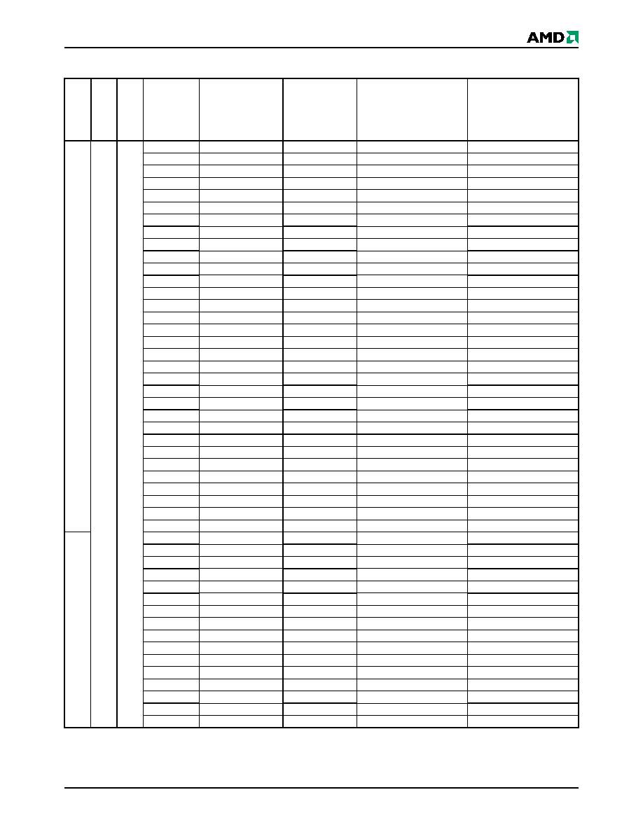
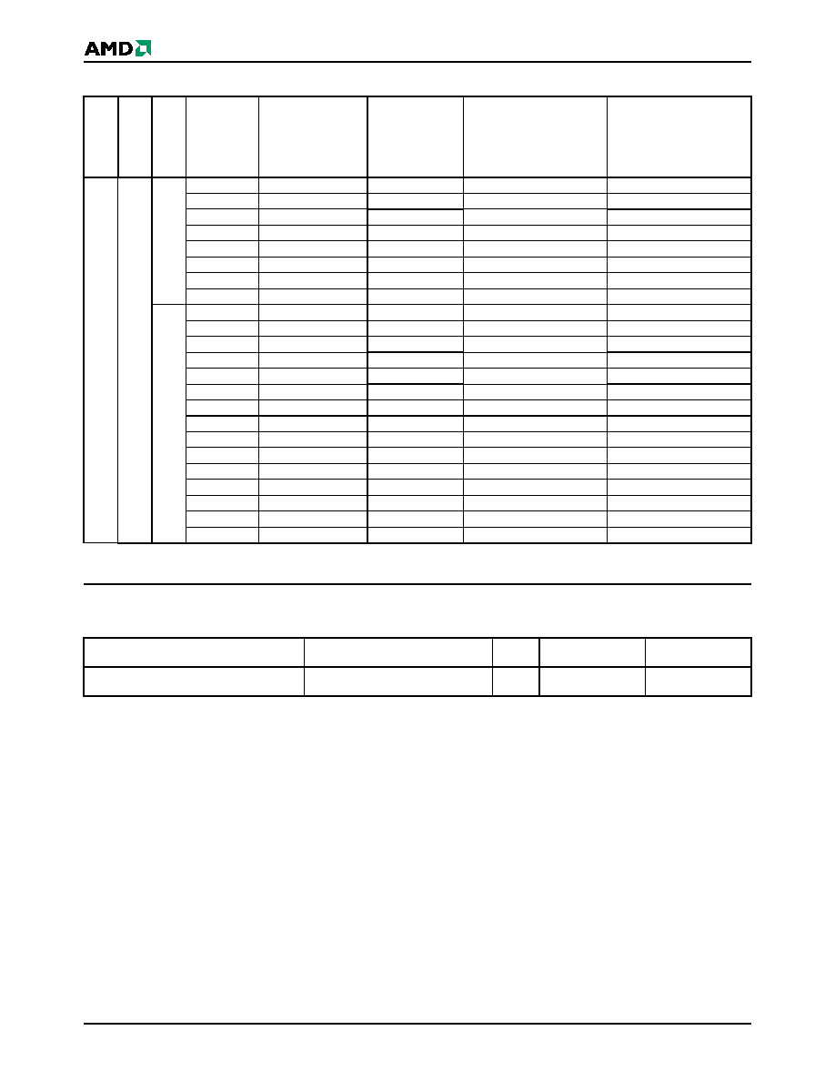
Table 3. Top Boot Sector Addresses
Am2
9
DL32
4DT
Am2
9
DL32
3DT
Am2
9
DL32
2DT
Sector
Sector Address
A20≠A12
Sector Size
(Kbytes/Kwords)
(x8)
Address Range
(x16)
Address Range
Bank
2
Ban
k
2
Ban
k
2
SA0
000000xxx
64/32
000000h≠00FFFFh
000000h≠07FFFh
SA1
000001xxx
64/32
010000h≠01FFFFh
008000h≠0FFFFh
SA2
000010xxx
64/32
020000h≠02FFFFh
010000h≠17FFFh
SA3
000011xxx
64/32
030000h≠03FFFFh
018000h≠01FFFFh
SA4
000100xxx
64/32
040000h≠04FFFFh
020000h≠027FFFh
SA5
000101xxx
64/32
050000h≠05FFFFh
028000h≠02FFFFh
SA6
000110xxx
64/32
060000h≠06FFFFh
030000h≠037FFFh
SA7
000111xxx
64/32
070000h≠07FFFFh
038000h≠03FFFFh
SA8
001000xxx
64/32
080000h≠08FFFFh
040000h≠047FFFh
SA9
001001xxx
64/32
090000h≠09FFFFh
048000h≠04FFFFh
SA10
001010xxx
64/32
0A0000h≠0AFFFFh
050000h≠057FFFh
SA11
001011xxx
64/32
0B0000h≠0BFFFFh
058000h≠05FFFFh
SA12
001100xxx
64/32
0C0000h≠0CFFFFh
060000h≠067FFFh
SA13
001101xxx
64/32
0D0000h≠0DFFFFh
068000h≠06FFFFh
SA14
001110xxx
64/32
0E0000h≠0EFFFFh
070000h≠077FFFh
SA15
001111xxx
64/32
0F0000h≠0FFFFFh
078000h≠07FFFFh
SA16
010000xxx
64/32
100000h≠10FFFFh
080000h≠087FFFh
SA17
010001xxx
64/32
110000h≠11FFFFh
088000h≠08FFFFh
SA18
010010xxx
64/32
120000h≠12FFFFh
090000h≠097FFFh
SA19
010011xxx
64/32
130000h≠13FFFFh
098000h≠09FFFFh
SA20
010100xxx
64/32
140000h≠14FFFFh
0A0000h≠0A7FFFh
SA21
010101xxx
64/32
150000h≠15FFFFh
0A8000h≠0AFFFFh
SA22
010110xxx
64/32
160000h≠16FFFFh
0B0000h≠0B7FFFh
SA23
010111xxx
64/32
170000h≠17FFFFh
0B8000h≠0BFFFFh
SA24
011000xxx
64/32
180000h≠18FFFFh
0C0000h≠0C7FFFh
SA25
011001xxx
64/32
190000h≠19FFFFh
0C8000h≠0CFFFFh
SA26
011010xxx
64/32
1A0000h≠1AFFFFh
0D0000h≠0D7FFFh
SA27
011011xxx
64/32
1B0000h≠1BFFFFh
0D8000h≠0DFFFFh
SA28
011100xxx
64/32
1C0000h≠1CFFFFh
0E0000h≠0E7FFFh
SA29
011101xxx
64/32
1D0000h≠1DFFFFh
0E8000h≠0EFFFFh
SA30
011110xxx
64/32
1E0000h≠1EFFFFh
0F0000h≠0F7FFFh
SA31
011111xxx
64/32
1F0000h≠1FFFFFh
0F8000h≠0FFFFFh
Ba
nk 1
SA32
100000xxx
64/32
200000h≠20FFFFh
100000h≠107FFFh
SA33
100001xxx
64/32
210000h≠21FFFFh
108000h≠10FFFFh
SA34
100010xxx
64/32
220000h≠22FFFFh
110000h≠117FFFh
SA35
100011xxx
64/32
230000h≠23FFFFh
118000h≠11FFFFh
SA36
100100xxx
64/32
240000h≠24FFFFh
120000h≠127FFFh
SA37
100101xxx
64/32
250000h≠25FFFFh
128000h≠12FFFFh
SA38
100110xxx
64/32
260000h≠26FFFFh
130000h≠137FFFh
SA39
100111xxx
64/32
270000h≠27FFFFh
138000h≠13FFFFh
SA40
101000xxx
64/32
280000h≠28FFFFh
140000h≠147FFFh
SA41
101001xxx
64/32
290000h≠29FFFFh
148000h≠14FFFFh
SA42
101010xxx
64/32
2A0000h≠2AFFFFh
150000h≠157FFFh
SA43
101011xxx
64/32
2B0000h≠2BFFFFh
158000h≠15FFFFh
SA44
101100xxx
64/32
2C0000h≠2CFFFFh
160000h≠167FFFh
SA45
101101xxx
64/32
2D0000h≠2DFFFFh
168000h≠16FFFFh
SA46
101110xxx
64/32
2E0000h≠2EFFFFh
170000h≠177FFFh
SA47
101111xxx
64/32
2F0000h≠2FFFFFh
178000h≠17FFFFh
12
Am29DL322D/323D/324D
June 10, 2003
Note: The address range is A20:A-1 in byte mode (BYTE#=V
IL
) or A20:A0 in word mode (BYTE#=V
IH
). The bank address bits are A20≠A18 for
Am29DL322DT, A20 and A19 for Am29DL323DT, and A20 for Am29DL324DT.
Table 4. Top Boot SecSi
Sector Addresses
Bank 1
Bank 1
Bank 2
SA48
110000xxx
64/32
300000h≠30FFFFh
180000h≠187FFFh
SA49
110001xxx
64/32
310000h≠31FFFFh
188000h≠18FFFFh
SA50
110010xxx
64/32
320000h≠32FFFFh
190000h≠197FFFh
SA51
110011xxx
64/32
330000h≠33FFFFh
198000h≠19FFFFh
SA52
110100xxx
64/32
340000h≠34FFFFh
1A0000h≠1A7FFFh
SA53
110101xxx
64/32
350000h≠35FFFFh
1A8000h≠1AFFFFh
SA54
110110xxx
64/32
360000h≠36FFFFh
1B0000h≠1B7FFFh
SA55
110111xxx
64/32
370000h≠37FFFFh
1B8000h≠1BFFFFh
Bank 1
SA56
111000xxx
64/32
380000h≠38FFFFh
1C0000h≠1C7FFFh
SA57
111001xxx
64/32
390000h≠39FFFFh
1C8000h≠1CFFFFh
SA58
111010xxx
64/32
3A0000h≠3AFFFFh
1D0000h≠1D7FFFh
SA59
111011xxx
64/32
3B0000h≠3BFFFFh
1D8000h≠1DFFFFh
SA60
111100xxx
64/32
3C0000h≠3CFFFFh
1E0000h≠1E7FFFh
SA61
111101xxx
64/32
3D0000h≠3DFFFFh
1E8000h≠1EFFFFh
SA62
111110xxx
64/32
3E0000h≠3EFFFFh
1F0000h≠1F7FFFh
SA63
111111000
8/4
3F0000h≠3F1FFFh
1F8000h≠1F8FFFh
SA64
111111001
8/4
3F2000h≠3F3FFFh
1F9000h≠1F9FFFh
SA65
111111010
8/4
3F4000h≠3F5FFFh
1FA000h≠1FAFFFh
SA66
111111011
8/4
3F6000h≠3F7FFFh
1FB000h≠1FBFFFh
SA67
111111100
8/4
3F8000h≠3F9FFFh
1FC000h≠1FCFFFh
SA68
111111101
8/4
3FA000h≠3FBFFFh
1FD000h≠1FDFFFh
SA69
111111110
8/4
3FC000h≠3FDFFFh
1FE000h≠1FEFFFh
SA70
111111111
8/4
3FE000h≠3FFFFFh
1FF000h≠1FFFFFh
Table 3. Top Boot Sector Addresses (Continued)
Am29DL324DT
Am29DL323DT
Am29DL322DT
Sector
Sector Address
A20≠A12
Sector Size
(Kbytes/Kwords)
(x8)
Address Range
(x16)
Address Range
Device
Sector Address
A20≠A12
Sector
Size
(x8)
Address Range
(x16)
Address Range
Am29DL322DT, Am29DL323DT,
Am29DL324DT
111111xxx
64/32
3F0000h≠3FFFFFh
1F8000h≠1FFFFh
June 10, 2003
Am29DL322D/323D/324D
13
Table 5. Bottom Boot Sector Addresses
Am29DL324DB
Am29DL323DB
Am29DL322DB
Sector
Sector Address
A20≠A12
Sector Size
(Kbytes/Kwords)
(x8)
Address Range
(x16)
Address Range
Ban
k
1
Bank 1
Bank 1
SA0
000000000
8/4
000000h-001FFFh
000000h≠000FFFh
SA1
000000001
8/4
002000h-003FFFh
001000h≠001FFFh
SA2
000000010
8/4
004000h-005FFFh
002000h≠002FFFh
SA3
000000011
8/4
006000h-007FFFh
003000h≠003FFFh
SA4
000000100
8/4
008000h-009FFFh
004000h≠004FFFh
SA5
000000101
8/4
00A000h-00BFFFh
005000h≠005FFFh
SA6
000000110
8/4
00C000h-00DFFFh
006000h≠006FFFh
SA7
000000111
8/4
00E000h-00FFFFh
007000h≠007FFFh
SA8
000001xxx
64/32
010000h-01FFFFh
008000h≠00FFFFh
SA9
000010xxx
64/32
020000h-02FFFFh
010000h≠017FFFh
SA10
000011xxx
64/32
030000h-03FFFFh
018000h≠01FFFFh
SA11
000100xxx
64/32
040000h-04FFFFh
020000h≠027FFFh
SA12
000101xxx
64/32
050000h-05FFFFh
028000h≠02FFFFh
SA13
000110xxx
64/32
060000h-06FFFFh
030000h≠037FFFh
SA14
000111xxx
64/32
070000h-07FFFFh
038000h≠03FFFFh
Bank 2
SA15
001000xxx
64/32
080000h-08FFFFh
040000h≠047FFFh
SA16
001001xxx
64/32
090000h-09FFFFh
048000h≠04FFFFh
SA17
001010xxx
64/32
0A0000h-0AFFFFh
050000h≠057FFFh
SA18
001011xxx
64/32
0B0000h-0BFFFFh
058000h≠05FFFFh
SA19
001100xxx
64/32
0C0000h-0CFFFFh
060000h≠067FFFh
SA20
001101xxx
64/32
0D0000h-0DFFFFh
068000h≠06FFFFh
SA21
001110xxx
64/32
0E0000h-0EFFFFh
070000h≠077FFFh
SA22
001111xxx
64/32
0F0000h-0FFFFFh
078000h≠07FFFFh
Bank 2
SA23
010000xxx
64/32
100000h-10FFFFh
080000h≠087FFFh
SA24
010001xxx
64/32
110000h-11FFFFh
088000h≠08FFFFh
SA25
010010xxx
64/32
120000h-12FFFFh
090000h≠097FFFh
SA26
010011xxx
64/32
130000h-13FFFFh
098000h≠09FFFFh
SA27
010100xxx
64/32
140000h-14FFFFh
0A0000h≠0A7FFFh
SA28
010101xxx
64/32
150000h-15FFFFh
0A8000h≠0AFFFFh
SA29
010110xxx
64/32
160000h-16FFFFh
0B0000h≠0B7FFFh
SA30
010111xxx
64/32
170000h-17FFFFh
0B8000h≠0BFFFFh
SA31
011000xxx
64/32
180000h-18FFFFh
0C0000h≠0C7FFFh
SA32
011001xxx
64/32
190000h-19FFFFh
0C8000h≠0CFFFFh
SA33
011010xxx
64/32
1A0000h-1AFFFFh
0D0000h≠0D7FFFh
SA34
011011xxx
64/32
1B0000h-1BFFFFh
0D8000h≠0DFFFFh
SA35
011100xxx
64/32
1C0000h-1CFFFFh
0E0000h≠0E7FFFh
SA36
011101xxx
64/32
1D0000h-1DFFFFh
0E8000h≠0EFFFFh
SA37
011110xxx
64/32
1E0000h-1EFFFFh
0F0000h≠0F7FFFh
SA38
011111xxx
64/32
1F0000h-1FFFFFh
0F8000h≠0FFFFFh
Ba
nk 2
SA39
100000xxx
64/32
200000h-20FFFFh
100000h≠107FFFh
SA40
100001xxx
64/32
210000h-21FFFFh
108000h≠10FFFFh
SA41
100010xxx
64/32
220000h-22FFFFh
110000h≠117FFFh
SA42
100011xxx
64/32
230000h-23FFFFh
118000h≠11FFFFh
SA43
100100xxx
64/32
240000h-24FFFFh
120000h≠127FFFh
SA44
100101xxx
64/32
250000h-25FFFFh
128000h≠12FFFFh
SA45
100110xxx
64/32
260000h-26FFFFh
130000h≠137FFFh
SA46
100111xxx
64/32
270000h-27FFFFh
138000h≠13FFFFh
SA47
101000xxx
64/32
280000h-28FFFFh
140000h≠147FFFh
14
Am29DL322D/323D/324D
June 10, 2003
Note: The address range is A20:A-1 in byte mode (BYTE#=V
IL
) or A20:A0 in word mode (BYTE#=V
IH
). The bank address bits
are A20≠A18 for Am29DL322DB, A20 and A19 for Am29DL323DB, and A20 for Am29DL324DB.
Table 6. Bottom Boot SecSi
Sector Addresses
Bank 2
Bank 2
Bank 2
SA48
101001xxx
64/32
290000h-29FFFFh
148000h≠14FFFFh
SA49
101010xxx
64/32
2A0000h-2AFFFFh
150000h≠157FFFh
SA50
101011xxx
64/32
2B0000h-2BFFFFh
158000h≠15FFFFh
SA51
101100xxx
64/32
2C0000h-2CFFFFh
160000h≠167FFFh
SA52
101101xxx
64/32
2D0000h-2DFFFFh
168000h≠16FFFFh
SA53
101110xxx
64/32
2E0000h-2EFFFFh
170000h≠177FFFh
SA54
101111xxx
64/32
2F0000h-2FFFFFh
178000h≠17FFFFh
SA55
111000xxx
64/32
300000h-30FFFFh
180000h≠187FFFh
SA56
110001xxx
64/32
310000h-31FFFFh
188000h≠18FFFFh
SA57
110010xxx
64/32
320000h-32FFFFh
190000h≠197FFFh
SA58
110011xxx
64/32
330000h-33FFFFh
198000h≠19FFFFh
SA59
110100xxx
64/32
340000h-34FFFFh
1A0000h≠1A7FFFh
SA60
110101xxx
64/32
350000h-35FFFFh
1A8000h≠1AFFFFh
SA61
110110xxx
64/32
360000h-36FFFFh
1B0000h≠1B7FFFh
SA62
110111xxx
64/32
370000h-37FFFFh
1B8000h≠1BFFFFh
SA63
111000xxx
64/32
380000h-38FFFFh
1C0000h≠1C7FFFh
SA64
111001xxx
64/32
390000h-39FFFFh
1C8000h≠1CFFFFh
SA65
111010xxx
64/32
3A0000h-3AFFFFh
1D0000h≠1D7FFFh
SA66
111011xxx
64/32
3B0000h-3BFFFFh
1D8000h≠1DFFFFh
SA67
111100xxx
64/32
3C0000h-3CFFFFh
1E0000h≠1E7FFFh
SA68
111101xxx
64/32
3D0000h-3DFFFFh
1E8000h≠1EFFFFh
SA69
111110xxx
64/32
3E0000h-3EFFFFh
1F0000h≠1F7FFFh
SA70
111111xxx
64/32
3F0000h-3FFFFFh
1F8000h≠1FFFFFh
Device
Sector Address
A20≠A12
Sector
Size
(x8)
Address Range
(x16)
Address Range
Am29DL322DB, Am29DL323DB
,
Am29DL324DB
000000xxx
64/32
000000h-00FFFFh
00000h-07FFFh
Table 5. Bottom Boot Sector Addresses (Continued)
Am29DL324DB
Am29DL323DB
Am29DL322DB
Sector
Sector Address
A20≠A12
Sector Size
(Kbytes/Kwords)
(x8)
Address Range
(x16)
Address Range
June 10, 2003
Am29DL322D/323D/324D
15
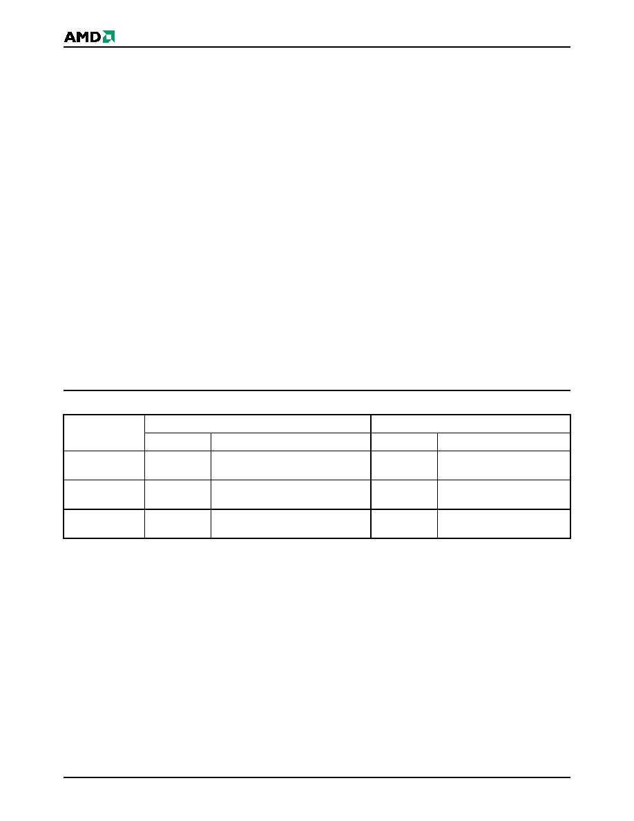
Autoselect Mode
The autoselect mode provides manufacturer and de-
vice identification, and sector protection verification,
through identifier codes output on DQ7≠DQ0. This
mode is primarily intended for programming equip-
ment to automatically match a device to be pro-
grammed with its corresponding programming
algorithm. However, the autoselect codes can also be
accessed in-system through the command register.
When using programming equipment, the autoselect
mode requires V
ID
(8.5 V to 12.5 V) on address pin A9.
Address pins A6, A1, and A0 must be as shown in
Table 7. In addition, when verifying sector protection,
the sector address must appear on the appropriate
highest order address bits (see Tables 3≠6). Table 7
shows the remaining address bits that are don't care.
When all necessary bits have been set as required,
the programming equipment may then read the corre-
sponding identifier code on DQ7≠DQ0.
To access the autoselect codes in-system, the host
system can issue the autoselect command via the
command register, as shown in Table 14. This method
does not require V
ID
. Refer to the Autoselect Com-
mand Sequence section for more information.
Table 7. Autoselect Codes, (High Voltage Method)
Legend: T = Top Boot Block, B = Bottom Boot Block, L = Logic Low = V
IL
, H = Logic High = V
IH
, BA = Bank Address, SA = Sector Address, X
= Don't care.
Description
CE# OE# WE#
A20
to
A12
A11
to
A10
A9
A8
to
A7
A6
A5
to
A2
A1
A0
DQ8 to DQ15
DQ7
to
DQ0
BYTE#
= V
IH
BYTE#
= V
IL
Manufacturer ID: AMD
L
L
H
BA
X
V
ID
X
L
X
L
L
X
X
01h
Device ID: Am29DL322D
L
L
H
BA
X
V
ID
X
L
X
L
H
22h
X
55h (T), 56h (B)
Device ID: Am29DL323D
L
L
H
BA
X
V
ID
X
L
X
L
H
22h
X
50h (T), 53h (B)
Device ID: Am29DL324D
L
L
H
BA
X
V
ID
X
L
X
L
H
22h
X
5Ch (T), 5Fh (B)
Sector Protection
Verification
L
L
H
SA
X
V
ID
X
L
X
H
L
X
X
01h (protected),
00h (unprotected)
SecSi
Indicator Bit
(DQ7)
L
L
H
BA
X
V
ID
X
L
X
H
H
X
X
81h (factory locked),
01h (not factory
locked)
16
Am29DL322D/323D/324D
June 10, 2003
Sector/Sector Block Protection and
Unprotection
(Note: For the following discussion, the term "sector"
applies to both sectors and sector blocks. A sector
block consists of two or more adjacent sectors that are
protected or unprotected at the same time (see Tables
8 and 9).
The hardware sector protection feature disables both
program and erase operations in any sector. The
hardware sector unprotection feature re-enables both
program and erase operations in previously protected
sectors. Sector protection/unprotection can be imple-
mented via two methods.
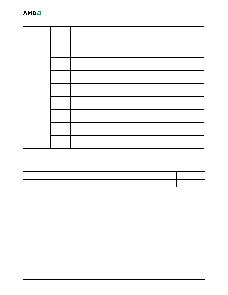
Table 8. Top Boot Sector/Sector Block Addresses
for Protection/Unprotection
Table 9. Bottom Boot Sector/Sector Block
Addresses for Protection/Unprotection
The primary method requires V
ID
on the RESET# pin
only, and can be implemented either in-system or via
programming equipment. Figure 2 shows the algo-
rithms and Figure 25 shows the timing diagram. This
method uses standard microprocessor bus cycle tim-
ing. For sector unprotect, all unprotected sectors must
first be protected prior to the first sector unprotect write
cycle.
The sector unprotect algorithm unprotects all sectors
in parallel. All previously protected sectors must be in-
dividually re-protected. To change data in protected
sectors efficiently, the temporary sector unprotect
function is available. See "Temporary Sector Unpro-
tect".
Sector
A20≠A12
Sector/
Sector Block Size
SA0
000000XXX
64 Kbytes
SA1-SA3
000001XXX,
000010XXX
000011XXX
192 (3x64) Kbytes
SA4-SA7
0001XXXXX
256 (4x64) Kbytes
SA8-SA11
0010XXXXX
256 (4x64) Kbytes
SA12-SA15
0011XXXXX
256 (4x64) Kbytes
SA16-SA19
0100XXXXX
256 (4x64) Kbytes
SA20-SA23
0101XXXXX
256 (4x64) Kbytes
SA24-SA27
0110XXXXX
256 (4x64) Kbytes
SA28-SA31
0111XXXXX
256 (4x64) Kbytes
SA32-SA35
1000XXXXX
256 (4x64) Kbytes
SA36-SA39
1001XXXXX
256 (4x64) Kbytes
SA40-SA43
1010XXXXX
256 (4x64) Kbytes
SA44-SA47
1011XXXXX
256 (4x64) Kbytes
SA48-SA51
1100XXXXX
256 (4x64) Kbytes
SA52-SA55
1101XXXXX
256 (4x64) Kbytes
SA56-SA59
1110XXXXX
256 (4x64) Kbytes
SA60-SA62
111100XXX,
111101XXX,
111110XXX
192 (4x64) Kbytes
SA63
111111000
8 Kbytes
SA64
111111001
8 Kbytes
SA65
111111010
8 Kbytes
SA66
111111011
8 Kbytes
SA67
111111100
8 Kbytes
SA68
111111101
8 Kbytes
SA69
111111110
8 Kbytes
SA70
111111111
8 Kbytes
Sector
A20≠A12
Sector/Sector Block
Size
SA70
111111XXX
64 Kbytes
SA69-SA67
111110XXX,
111101XXX,
111100XXX
192 (3x64) Kbytes
SA66-SA63
1110XXXXX
256 (4x64) Kbytes
SA62-SA59
1101XXXXX
256 (4x64) Kbytes
SA58-SA55
1100XXXXX
256 (4x64) Kbytes
SA54-SA51
1011XXXXX
256 (4x64) Kbytes
SA50-SA47
1010XXXXX
256 (4x64) Kbytes
SA46-SA43
1001XXXXX
256 (4x64) Kbytes
SA42-SA39
1000XXXXX
256 (4x64) Kbytes
SA38-SA35
0111XXXXX
256 (4x64) Kbytes
SA34-SA31
0110XXXXX
256 (4x64) Kbytes
SA30-SA27
0101XXXXX
256 (4x64) Kbytes
SA26-SA23
0100XXXXX
256 (4x64) Kbytes
SA22≠SA19
0011XXXXX
256 (4x64) Kbytes
SA18-SA15
0010XXXXX
256 (4x64) Kbytes
SA14-SA11
0001XXXXX
256 (4x64) Kbytes
SA10-SA8
000011XXX,
000010XXX,
000001XXX
192 (3x64) Kbytes
SA7
000000111
8 Kbytes
SA6
000000110
8 Kbytes
SA5
000000101
8 Kbytes
SA4
000000100
8 Kbytes
SA3
000000011
8 Kbytes
SA2
000000010
8 Kbytes
SA1
000000001
8 Kbytes
SA0
000000000
8 Kbytes
June 10, 2003
Am29DL322D/323D/324D
17
The alternate method intended only for programming
equipment requires V
ID
on address pin A9 and OE#.
This method is compatible with programmer routines
written for earlier 3.0 volt-only AMD flash devices.
Publication number 22244 contains further details;
contact an AMD representative to request a copy.
The device is shipped with all sectors unprotected.
AMD offers the option of programming and protecting
sectors at its factory prior to shipping the device
through AMD's ExpressFlashTM Service. Contact an
AMD representative for details.
It is possible to determine whether a sector is pro-
tected or unprotected. See the Autoselect Mode sec-
tion for details.
Write Protect (WP#)
The Write Protect function provides a hardware
method of protecting certain boot sectors without
using V
ID
. This function is one of two provided by the
WP#/ACC pin.
If the system asserts V
IL
on the WP#/ACC pin, the de-
vice disables program and erase functions in the two
"outermost" 8 Kbyte boot sectors independently of
whether those sectors were protected or unprotected
using the method described in "Sector/Sector Block
Protection and Unprotection". The two outermost 8
Kbyte boot sectors are the two sectors containing the
lowest addresses in a bottom-boot-configured device,
or the two sectors containing the highest addresses in
a top-boot-configured device.
If the system asserts V
IH
on the WP#/ACC pin, the de-
vice reverts to whether the two outermost 8K Byte
boot sectors were last set to be protected or unpro-
tected. That is, sector protection or unprotection for
these two sectors depends on whether they were last
protected or unprotected using the method described
in "Sector/Sector Block Protection and Unprotection".
Note that the WP#/ACC pin must not be left floating or
unconnected; inconsistent behavior of the device may
result.
Temporary Sector Unprotect
(Note: For the following discussion, the term "sector"
applies to both sectors and sector blocks. A sector
block consists of two or more adjacent sectors that are
protected or unprotected at the same time (see Tables
8 and 9).
This feature allows temporary unprotection of previ-
ously protected sectors to change data in-system. The
Sector Unprotect mode is activated by setting the RE-
SET# pin to V
ID
(8.5 V ≠ 12.5 V). During this mode, for-
merly protected sectors can be programmed or erased
by selecting the sector addresses. Once V
ID
is re-
moved from the RESET# pin, all the previously pro-
tected sectors are protected again. Figure 1 shows the
algorithm, and Figure 24 shows the timing diagrams,
for this feature.
Figure 1. Temporary Sector Unprotect Operation
START
Perform Erase or
Program Operations
RESET# = V
IH
Temporary Sector
Unprotect Completed
(Note 2)
RESET# = V
ID
(Note 1)
Notes:
1. All protected sectors unprotected (If WP#/ACC = V
IL
,
outermost boot sectors will remain protected).
2. All previously protected sectors are protected once
again.
18
Am29DL322D/323D/324D
June 10, 2003
Figure 2. In-System Sector Protection/
Sector Unprotection Algorithms
Sector Protect:
Write 60h to sector
address with
A6 = 0, A1 = 1,
A0 = 0
Set up sector
address
Wait 150 µs
Verify Sector
Protect: Write 40h
to sector address
with A6 = 0,
A1 = 1, A0 = 0
Read from
sector address
with A6 = 0,
A1 = 1, A0 = 0
START
PLSCNT = 1
RESET# = V
ID
Wait 1
µ
s
First Write
Cycle = 60h?
Data = 01h?
Remove V
ID
from RESET#
Write reset
command
Sector Protect
complete
Yes
Yes
No
PLSCNT
= 25?
Yes
Device failed
Increment
PLSCNT
Temporary Sector
Unprotect Mode
No
Sector Unprotect:
Write 60h to any
address with
A6 = 1, A1 = 1,
A0 = 0
Set up first sector
address
Wait 15 ms
Verify Sector
Unprotect: Write
40h to sector
address with
A6 = 1, A1 = 1,
A0 = 0
Read from
sector address
with A6 = 1,
A1 = 1, A0 = 0
START
PLSCNT = 1
RESET# = V
ID
Wait 1
µ
s
Data = 00h?
Last sector
verified?
Remove V
ID
from RESET#
Write reset
command
Sector Unprotect
complete
Yes
No
PLSCNT
= 1000?
Yes
Device failed
Increment
PLSCNT
Temporary Sector
Unprotect Mode
No
All sectors
protected?
Yes
Protect all sectors:
The indicated portion
of the sector protect
algorithm must be
performed for all
unprotected sectors
prior to issuing the
first sector
unprotect address
Set up
next sector
address
No
Yes
No
Yes
No
No
Yes
No
Sector Protect
Algorithm
Sector Unprotect
Algorithm
First Write
Cycle = 60h?
Protect another
sector?
Reset
PLSCNT = 1

June 10, 2003
Am29DL322D/323D/324D
19
SecSi
(Secured Silicon) Sector
Flash Memory Region
The SecSi (Secured Silicon) Sector feature provides a
Flash memory region that enables permanent part
identification through an Electronic Serial Number
(ESN). The SecSi Sector uses a SecSi Sector Indica-
tor Bit (DQ7) to indicate whether or not the SecSi Sec-
tor is locked when shipped from the factory. This bit is
permanently set at the factory and cannot be changed,
which prevents cloning of a factory locked part. This
ensures the security of the ESN once the product is
shipped to the field. Current version of device has
64 Kbytes; future versions will have only 256
bytes. This should be considered during system
design.
AMD offers the device with the SecSi Sector either
factory locked or customer lockable. The fac-
tory-locked version is always protected when shipped
from the factory, and has the SecSi (Secured Silicon)
Sector Indicator Bit permanently set to a "1." The cus-
tomer-lockable version is shipped with the SecSi Sec-
tor unprotected, allowing customers to utilize the that
sector in any manner they choose. The customer-lock-
able version has the SecSi (Secured Silicon) Sector
Indicator Bit permanently set to a "0." Thus, the SecSi
Sector Indicator Bit prevents customer-lockable de-
vices from being used to replace devices that are fac-
tory locked.
The system accesses the SecSi Sector through a
command sequence (see "Enter SecSi
Sector/Exit
SecSi Sector Command Sequence"). After the system
has written the Enter SecSi Sector command se-
quence, it may read the SecSi Sector by using the ad-
dresses normally occupied by the boot sectors. This
mode of operation continues until the system issues
the Exit SecSi Sector command sequence, or until
power is removed from the device. On power-up, or
following a hardware reset, the device reverts to send-
ing commands to the boot sectors.
Factory Locked: SecSi Sector Programmed and
Protected At the Factory
In a factory locked device, the SecSi Sector is pro-
tected when the device is shipped from the factory.
The SecSi Sector cannot be modified in any way. The
device is available preprogrammed with one of the fol-
lowing:
A random, secure ESN only
Customer code through the ExpressFlash service
Both a random, secure ESN and customer code
through the ExpressFlash service.
In devices that have an ESN, a Bottom Boot device
w i l l h a v e t h e 1 6 - b y t e E S N a t a d d r e s s e s
0 0 0 0 0 0 h ≠ 0 0 0 0 0 7 h i n w o r d m o d e ( o r
000000h≠00000Fh in byte mode). In the Top Boot de-
vice the ESN will be at addresses 1F8000h≠1F8007h
in word mode (or addresses 3F0000h≠3F000Fh in
byte mode). Note that in upcoming top boot versions
of this device, the ESN will be located at addresses
1FF000h≠1FF007h in word mode (or addresses
3FE000h≠3FE00Fh in byte mode).
Customers may opt to have their code programmed by
AMD through the AMD ExpressFlash service. AMD
programs the customer's code, with or without the ran-
dom ESN. The devices are then shipped from AMD's
factory with the SecSi Sector permanently locked.
Contact an AMD representative for details on using
AMD's ExpressFlash service.
Customer Lockable: SecSi Sector NOT
Programmed or Protected At the Factory
If the security feature is not required, the SecSi Sector
can be treated as an additional Flash memory space,
expanding the size of the available Flash array. Cur-
rent version of device has 64 Kbytes; future ver-
sions will have only 256 bytes. This should be
considered during system design. Additionally,
note the change in the location of the ESN in up-
coming top boot factory locked devices. The SecSi
Sector can be read, programmed, and erased as often
as required. (Note that in upcoming versions of this
device, the SecSi Sector erase function will not be
available.) Note that the accelerated programming
(ACC) and unlock bypass functions are not available
when programming the SecSi Sector.
The SecSi Sector area can be protected using one of
the following procedures:
Write the three-cycle Enter SecSi Sector Region
command sequence, and then follow the in-system
sector protect algorithm as shown in Figure 2, ex-
cept that RESET# may be at either V
IH
or V
ID
. This
allows in-system protection of the SecSi Sector
without raising any device pin to a high voltage.
Note that this method is only applicable to the SecSi
Sector
Write the three-cycle Enter SecSi Sector Region
command sequence, and then use the alternate
method of sector protection described in the "Sec-
tor/Sector Block Protection and Unprotection" sec-
tion.
Once the SecSi Sector is locked and verified, the sys-
tem must write the Exit SecSi Sector Region com-
mand sequence to return to reading and writing the
remainder of the array.
The SecSi Sector protection must be used with cau-
tion since, once protected, there is no procedure avail-
able for unprotecting the SecSi Sector area and none
of the bits in the SecSi Sector memory space can be
modified in any way.
20
Am29DL322D/323D/324D
June 10, 2003
Hardware Data Protection
The command sequence requirement of unlock cycles
for programming or erasing provides data protection
against inadvertent writes (refer to Table 14 for com-
mand definitions). In addition, the following hardware
data protection measures prevent accidental erasure
or programming, which might otherwise be caused by
spurious system level signals during V
CC
power-up
and power-down transitions, or from system noise.
Low V
CC
Write Inhibit
When V
CC
is less than V
LKO
, the device does not ac-
cept any write cycles. This protects data during V
CC
power-up and power-down. The command register
and all internal program/erase circuits are disabled,
and the device resets to the read mode. Subsequent
writes are ignored until V
CC
is greater than V
LKO
. The
system must provide the proper signals to the control
pins to prevent unintentional writes when V
CC
is
greater than V
LKO
.
Write Pulse "Glitch" Protection
Noise pulses of less than 5 ns (typical) on OE#, CE#
or WE# do not initiate a write cycle.
Logical Inhibit
Write cycles are inhibited by holding any one of OE# =
V
IL
, CE# = V
IH
or WE# = V
IH
. To initiate a write cycle,
CE# and WE# must be a logical zero while OE# is a
logical one.
Power-Up Write Inhibit
If WE# = CE# = V
IL
and OE# = V
IH
during power up,
the device does not accept commands on the rising
edge of WE#. The internal state machine is automati-
cally reset to the read mode on power-up.
COMMON FLASH MEMORY INTERFACE
(CFI)
The Common Flash Interface (CFI) specification out-
lines device and host system software interrogation
handshake, which allows specific vendor-specified
software algorithms to be used for entire families of
devices. Software support can then be device-inde-
pendent, JEDEC ID-independent, and forward- and
backward-compatible for the specified flash device
families. Flash vendors can standardize their existing
interfaces for long-term compatibility.
This device enters the CFI Query mode when the sys-
tem writes the CFI Query command, 98h, to address
55h in word mode (or address AAh in byte mode), any
time the device is ready to read array data. The
system can read CFI information at the addresses
given in Tables 10≠13. To terminate reading CFI data,
the system must write the reset command. The CFI
Query mode is not accessible when the device is exe-
cuting an Embedded Program or Embedded Erase al-
gorithm.
The system can also write the CFI query command
when the device is in the autoselect mode. The device
enters the CFI query mode, and the system can read
CFI data at the addresses given in Tables 10≠13. The
system must write the reset command to return the de-
vice to the autoselect mode.
For further information, please refer to the CFI Specifi-
cation and CFI Publication 100, available via the
World Wide Web at http://www.amd.com/prod-
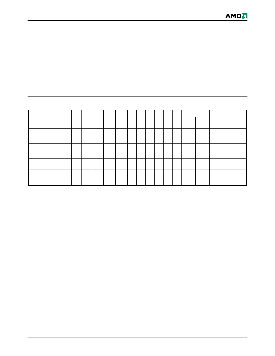
Table 10. CFI Query Identification String
Addresses
(Word Mode)
Addresses
(Byte Mode)
Data
Description
10h
11h
12h
20h
22h
24h
0051h
0052h
0059h
Query Unique ASCII string "QRY"
13h
14h
26h
28h
0002h
0000h
Primary OEM Command Set
15h
16h
2Ah
2Ch
0040h
0000h
Address for Primary Extended Table
17h
18h
2Eh
30h
0000h
0000h
Alternate OEM Command Set (00h = none exists)
19h
1Ah
32h
34h
0000h
0000h
Address for Alternate OEM Extended Table (00h = none exists)
June 10, 2003
Am29DL322D/323D/324D
21
Table 11. System Interface String
Table 12. Device Geometry Definition
Addresses
(Word Mode)
Addresses
(Byte Mode)
Data
Description
1Bh
36h
0027h
V
CC
Min. (write/erase)
D7≠D4: volt, D3≠D0: 100 millivolt
1Ch
38h
0036h
V
CC
Max. (write/erase)
D7≠D4: volt, D3≠D0: 100 millivolt
1Dh
3Ah
0000h
V
PP
Min. voltage (00h = no V
PP
pin present)
1Eh
3Ch
0000h
V
PP
Max. voltage (00h = no V
PP
pin present)
1Fh
3Eh
0004h
Typical timeout per single byte/word write 2
N
µs
20h
40h
0000h
Typical timeout for Min. size buffer write 2
N
µ
s (00h = not supported)
21h
42h
000Ah
Typical timeout per individual block erase 2
N
ms
22h
44h
0000h
Typical timeout for full chip erase 2
N
ms (00h = not supported)
23h
46h
0005h
Max. timeout for byte/word write 2
N
times typical
24h
48h
0000h
Max. timeout for buffer write 2
N
times typical
25h
4Ah
0004h
Max. timeout per individual block erase 2
N
times typical
26h
4Ch
0000h
Max. timeout for full chip erase 2
N
times typical (00h = not supported)
Addresses
(Word Mode)
Addresses
(Byte Mode)
Data
Description
27h
4Eh
0016h
Device Size = 2
N
byte
28h
29h
50h
52h
0000h
0000h
Flash Device Interface description (refer to CFI publication 100)
2Ah
2Bh
54h
56h
0000h
0000h
Max. number of bytes in multi-byte write = 2
N
(00h = not supported)
2Ch
58h
0002h
Number of Erase Block Regions within device
2Dh
2Eh
2Fh
30h
5Ah
5Ch
5Eh
60h
0007h
0000h
0020h
0000h
Erase Block Region 1 Information
(refer to the CFI specification or CFI publication 100)
31h
32h
33h
34h
62h
64h
66h
68h
003Eh
0000h
0000h
0001h
Erase Block Region 2 Information
35h
36h
37h
38h
6Ah
6Ch
6Eh
70h
0000h
0000h
0000h
0000h
Erase Block Region 3 Information
39h
3Ah
3Bh
3Ch
72h
74h
76h
78h
0000h
0000h
0000h
0000h
Erase Block Region 4 Information
22
Am29DL322D/323D/324D
June 10, 2003
Table 13. Primary Vendor-Specific Extended Query
Note:
The number of sectors in Bank 2 is device dependent.
Am29DL322 = 38h, Am29DL323 = 30h, Am29DL324 = 20h
COMMAND DEFINITIONS
Writing specific address and data commands or se-
quences into the command register initiates device op-
erations. Table 14 defines the valid register command
sequences. Writing incorrect address and data val-
ues or writing them in the improper sequence resets
the device to reading array data.
All addresses are latched on the falling edge of WE#
or CE#, whichever happens later. All data is latched
on the rising edge of WE# or CE#, whichever happens
first. Refer to the AC Characteristics section for timing
diagrams.
Reading Array Data
The device is automatically set to reading array data
after device power-up. No commands are required to
retrieve data. Each bank is ready to read array data
after completing an Embedded Program or Embedded
Erase algorithm.
After the device accepts an Erase Suspend command,
the corresponding bank enters the erase-sus-
pend-read mode, after which the system can read
data from any non-erase-suspended sector within the
same bank. After completing a programming operation
in the Erase Suspend mode, the system may once
Addresses
(Word Mode)
Addresses
(Byte Mode)
Data
Description
40h
41h
42h
80h
82h
84h
0050h
0052h
0049h
Query-unique ASCII string "PRI"
43h
86h
0031h
Major version number, ASCII
44h
88h
0031h
Minor version number, ASCII
45h
8Ah
0000h
Address Sensitive Unlock (Bits 1-0)
0 = Required, 1 = Not Required
Silicon Revision Number (Bits 7-2)
46h
8Ch
0002h
Erase Suspend
0 = Not Supported, 1 = To Read Only, 2 = To Read & Write
47h
8Eh
0001h
Sector Protect
0 = Not Supported, X = Number of sectors in per group
48h
90h
0001h
Sector Temporary Unprotect
00 = Not Supported, 01 = Supported
49h
92h
0004h
Sector Protect/Unprotect scheme
04 = 29LV800 mode
4Ah
94h
00XXh
(See Note)
Simultaneous Operation
00 = Not Supported, X = Number of Sectors in Bank 2 (Uniform Bank)
4Bh
96h
0000h
Burst Mode Type
00 = Not Supported, 01 = Supported
4Ch
98h
0000h
Page Mode Type
00 = Not Supported, 01 = 4 Word Page, 02 = 8 Word Page
4Dh
9Ah
0085h
ACC (Acceleration) Supply Minimum
00h = Not Supported, D7-D4: Volt, D3-D0: 100 mV
4Eh
9Ch
0095h
ACC (Acceleration) Supply Maximum
00h = Not Supported, D7-D4: Volt, D3-D0: 100 mV
4Fh
9Eh
000Xh
Top/Bottom Boot Sector Flag
02h = Bottom Boot Device, 03h = Top Boot Device

June 10, 2003
Am29DL322D/323D/324D
23
again read array data with the same exception. See
the Erase Suspend/Erase Resume Commands sec-
tion for more information.
The system must issue the reset command to return a
bank to the read (or erase-suspend-read) mode if DQ5
goes high during an active program or erase opera-
tion, or if the bank is in the autoselect mode. See the
next section, Reset Command, for more information.
See also Requirements for Reading Array Data in the
Device Bus Operations section for more information.
The Read-Only Operations table provides the read pa-
rameters, and Figure 13 shows the timing diagram.
Reset Command
Writing the reset command resets the banks to the
read or erase-suspend-read mode. Address bits are
don't cares for this command.
The reset command may be written between the se-
quence cycles in an erase command sequence before
erasing begins. This resets the bank to which the sys-
tem was writing to the read mode. Once erasure be-
gins, however, the device ignores reset commands
until the operation is complete.
The reset command may be written between the
sequence cycles in a program command sequence
before programming begins. This resets the bank to
which the system was writing to the read mode. If the
program command sequence is written to a bank that
is in the Erase Suspend mode, writing the reset
command returns that bank to the erase-sus-
pend-read mode. Once programming begins, how-
ever, the device ignores reset commands until the
operation is complete.
The reset command may be written between the se-
quence cycles in an autoselect command sequence.
Once in the autoselect mode, the reset command
must be written to return to the read mode. If a bank
entered the autoselect mode while in the Erase Sus-
pend mode, writing the reset command returns that
bank to the erase-suspend-read mode.
If DQ5 goes high during a program or erase operation,
writing the reset command returns the banks to the
read mode (or erase-suspend-read mode if that bank
was in Erase Suspend).
Autoselect Command Sequence
The autoselect command sequence allows the host
system to access the manufacturer and device codes,
and determine whether or not a sector is protected.
Table 14 shows the address and data requirements.
This method is an alternative to that shown in Table 7,
which is intended for PROM programmers and re-
quires V
ID
on address pin A9. The autoselect com-
mand sequence may be written to an address within a
bank that is either in the read or erase-suspend-read
mode. The autoselect command may not be written
while the device is actively programming or erasing in
the other bank.
The autoselect command sequence is initiated by first
writing two unlock cycles. This is followed by a third
write cycle that contains the bank address and the au-
toselect command. The bank then enters the autose-
lect mode. The system may read at any address within
the same bank any number of times without initiating
another autoselect command sequence:
A read cycle at address (BA)XX00h (where BA is
the bank address) returns the manufacturer code.
A read cycle at address (BA)XX01h in word mode
(or (BA)XX02h in byte mode) returns the device
code.
A read cycle to an address containing a sector ad-
dress (SA) within the same bank, and the address
02h on A7≠A0 in word mode (or the address 04h on
A6≠A-1 in byte mode) returns 01h if the sector is
protected, or 00h if it is unprotected. (Refer to Ta-
bles 3≠6 for valid sector addresses).
The system must write the reset command to return to
the read mode (or erase-suspend-read mode if the
bank was previously in Erase Suspend).
Enter SecSi
Sector/Exit SecSi Sector
Command Sequence
The SecSi Sector region provides a secured data area
containing a random, sixteen-byte electronic serial
number (ESN). The system can access the SecSi
Sector region by issuing the three-cycle Enter SecSi
Sector command sequence. The device continues to
access the SecSi Sector region until the system is-
sues the four-cycle Exit SecSi Sector command se-
quence. The Exit SecSi Sector command sequence
returns the device to normal operation. The SecSi
Sector is not accessible when the device is executing
an Embedded Program or Embedded Erase algo-
rithm. Table 14 shows the address and data require-
ments for both command sequences. See also "SecSi
(Secured Silicon) Sector Flash Memory Region" for fur-
ther information.
Byte/Word Program Command Sequence
The system may program the device by word or byte,
depending on the state of the BYTE# pin. Program-
ming is a four-bus-cycle operation. The program com-
mand sequence is initiated by writing two unlock write
cycles, followed by the program set-up command. The
program address and data are written next, which in
turn initiate the Embedded Program algorithm. The
system is not required to provide further controls or
timings. The device automatically provides internally
generated program pulses and verifies the pro-
24
Am29DL322D/323D/324D
June 10, 2003
grammed cell margin. Table 14 shows the address
and data requirements for the byte program command
sequence.
When the Embedded Program algorithm is complete,
that bank then returns to the read mode and ad-
dresses are no longer latched. The system can deter-
mine the status of the program operation by using
DQ7, DQ6, or RY/BY#. Refer to the Write Operation
Status section for information on these status bits.
Any commands written to the device during the Em-
bedded Program Algorithm are ignored. Note that a
hardware reset immediately terminates the program
operation. The program command sequence should
be reinitiated once that bank has returned to the read
mode, to ensure data integrity.
Programming is allowed in any sequence and across
sector boundaries. A bit cannot be programmed
from "0" back to a "1." Attempting to do so may
cause that bank to set DQ5 = 1, or cause the DQ7 and
DQ6 status bits to indicate the operation was success-
ful. However, a succeeding read will show that the
data is still "0." Only erase operations can convert a
"0" to a "1."
Unlock Bypass Command Sequence
The unlock bypass feature allows the system to pro-
gram bytes or words to a bank faster than using the
standard program command sequence. The unlock
bypass command sequence is initiated by first writing
two unlock cycles. This is followed by a third write
cycle containing the unlock bypass command, 20h.
That bank then enters the unlock bypass mode. A
two-cycle unlock bypass program command sequence
is all that is required to program in this mode. The first
cycle in this sequence contains the unlock bypass pro-
gram command, A0h; the second cycle contains the
program address and data. Additional data is pro-
grammed in the same manner. This mode dispenses
with the initial two unlock cycles required in the stan-
dard program command sequence, resulting in faster
total programming time.
Table 14
shows the require-
ments for the command sequence.
During the unlock bypass mode, only the Unlock By-
pass Program and Unlock Bypass Reset commands
are valid. To exit the unlock bypass mode, the system
must issue the two-cycle unlock bypass reset com-
mand sequence. See
Table 14
for address and data
requirements.
The device offers accelerated program operations
through the WP#/ACC pin. When the system asserts
V
HH
on the WP#/ACC pin, the device automatically en-
ters the Unlock Bypass mode. The system may then
write the two-cycle Unlock Bypass program command
sequence. The device uses the higher voltage on the
WP#/ACC pin to accelerate the operation. Note that
the WP#/ACC pin must not be at V
HH
any operation
other than accelerated programming, or device dam-
age may result. In addition, the WP#/ACC pin must not
be left floating or unconnected; inconsistent behavior
of the device may result.
Figure 3 illustrates the algorithm for the program oper-
ation. Refer to the Erase and Program Operations
table in the AC Characteristics section for parameters,
and Figure 17 for timing diagrams.
Figure 3. Program Operation
Chip Erase Command Sequence
Chip erase is a six bus cycle operation. The chip erase
command sequence is initiated by writing two unlock
cycles, followed by a set-up command. Two additional
unlock write cycles are then followed by the chip erase
command, which in turn invokes the Embedded Erase
algorithm. The device does not require the system to
preprogram prior to erase. The Embedded Erase algo-
rithm automatically preprograms and verifies the entire
memory for an all zero data pattern prior to electrical
erase. The system is not required to provide any con-
START
Write Program
Command Sequence
Data Poll
from System
Verify Data?
No
Yes
Last Address?
No
Yes
Programming
Completed
Increment Address
Embedded
Program
algorithm
in progress
Note: See Table 14 for program command sequence.

June 10, 2003
Am29DL322D/323D/324D
25
trols or timings during these operations. Table 14
shows the address and data requirements for the chip
erase command sequence.
When the Embedded Erase algorithm is complete,
that bank returns to the read mode and addresses are
no longer latched. The system can determine the sta-
tus of the erase operation by using DQ7, DQ6, DQ2,
or RY/BY#. Refer to the Write Operation Status sec-
tion for information on these status bits.
Any commands written during the chip erase operation
are ignored. However, note that a hardware reset im-
mediately terminates the erase operation. If that oc-
curs, the chip erase command sequence should be
reinitiated once that bank has returned to reading
array data, to ensure data integrity.
Figure 4 illustrates the algorithm for the erase opera-
tion. Refer to the Erase and Program Operations ta-
bles in the AC Characteristics section for parameters,
and Figure 19 section for timing diagrams.
Sector Erase Command Sequence
Sector erase is a six bus cycle operation. The sector
erase command sequence is initiated by writing two
unlock cycles, followed by a set-up command. Two
additional unlock cycles are written, and are then fol-
lowed by the address of the sector to be erased, and
the sector erase command. Table 14 shows the ad-
dress and data requirements for the sector erase com-
mand sequence.
The device does not require the system to preprogram
prior to erase. The Embedded Erase algorithm auto-
matically programs and verifies the entire memory for
an all zero data pattern prior to electrical erase. The
system is not required to provide any controls or tim-
ings during these operations.
After the command sequence is written, a sector erase
time-out of 50 µs occurs. During the time-out period,
additional sector addresses and sector erase com-
mands (for sectors within the same bank) may be writ-
ten. Loading the sector erase buffer may be done in
any sequence, and the number of sectors may be from
one sector to all sectors. The time between these ad-
ditional cycles must be less than 50 µs, otherwise era-
sure may begin. Any sector erase address and
command following the exceeded time-out may or
may not be accepted. It is recommended that proces-
sor interrupts be disabled during this time to ensure all
commands are accepted. The interrupts can be re-en-
abled after the last Sector Erase command is written.
Any command other than Sector Erase or Erase
Suspend during the time-out period resets that
bank to the read mode. The system must rewrite the
command sequence and any additional addresses
and commands.
The system can monitor DQ3 to determine if the sec-
tor erase timer has timed out (See the section on DQ3:
Sector Erase Timer.). The time-out begins from the
rising edge of the final WE# pulse in the command
sequence.
When the Embedded Erase algorithm is complete, the
bank returns to reading array data and addresses are
no longer latched. Note that while the Embedded
Erase operation is in progress, the system can read
data from the non-erasing bank. The system can de-
termine the status of the erase operation by reading
DQ7, DQ6, DQ2, or RY/BY# in the erasing bank.
Refer to the Write Operation Status section for infor-
mation on these status bits.
Once the sector erase operation has begun, only the
Erase Suspend command is valid. All other com-
mands are ignored. However, note that a hardware
reset immediately terminates the erase operation. If
that occurs, the sector erase command sequence
should be reinitiated once that bank has returned to
reading array data, to ensure data integrity.
Figure 4 illustrates the algorithm for the erase opera-
tion. Refer to the Erase and Program Operations ta-
bles in the AC Characteristics section for parameters,
and Figure 19 section for timing diagrams.
Erase Suspend/Erase Resume
Commands
The Erase Suspend command, B0h, allows the sys-
tem to interrupt a sector erase operation and then read
data from, or program data to, any sector not selected
for erasure. The bank address is required when writing
this command. This command is valid only during the
sector erase operation, including the 50 µs time-out
period during the sector erase command sequence.
The Erase Suspend command is ignored if written dur-
ing the chip erase operation or Embedded Program
algorithm.
When the Erase Suspend command is written during
the sector erase operation, the device requires a max-
imum of 20 µs to suspend the erase operation. How-
ever, when the Erase Suspend command is written
during the sector erase time-out, the device immedi-
ately terminates the time-out period and suspends the
erase operation.
After the erase operation has been suspended, the
bank enters the erase-suspend-read mode. The sys-
tem can read data from or program data to any sector
not selected for erasure. (The device "erase sus-
pends" all sectors selected for erasure.) Reading at
any address within erase-suspended sectors pro-
duces status information on DQ7≠DQ0. The system
can use DQ7, or DQ6 and DQ2 together, to determine
if a sector is actively erasing or is erase-suspended.
26
Am29DL322D/323D/324D
June 10, 2003
Refer to the Write Operation Status section for infor-
mation on these status bits.
After an erase-suspended program operation is com-
plete, the bank returns to the erase-suspend-read
mode. The system can determine the status of the
program operation using the DQ7 or DQ6 status bits,
just as in the standard Byte Program operation.
Refer to the Write Operation Status section for more
information.
In the erase-suspend-read mode, the system can also
issue the autoselect command sequence. Refer to the
Autoselect Mode and Autoselect Command Sequence
sections for details.
To resume the sector erase operation, the system
must write the Erase Resume command. The bank
address of the erase-suspended bank is required
when writing this command. Further writes of the Re-
sume command are ignored. Another Erase Suspend
command can be written after the chip has resumed
erasing.
Figure 4. Erase Operation
START
Write Erase
Command Sequence
(Notes 1, 2)
Data Poll to Erasing
Bank from System
Data = FFh?
No
Yes
Erasure Completed
Embedded
Erase
algorithm
in progress
Notes:
1. See Table 14 for erase command sequence.
2. See the section on DQ3 for information on the sector
erase timer.
June 10, 2003
Am29DL322D/323D/324D
27
Table 14. Command Definitions
Legend:
X = Don't care
RA = Address of the memory location to be read.
RD = Data read from location RA during read operation.
PA = Address of the memory location to be programmed. Addresses
latch on the falling edge of the WE# or CE# pulse, whichever happens
later.
PD = Data to be programmed at location PA. Data latches on the rising
edge of WE# or CE# pulse, whichever happens first.
SA = Address of the sector to be verified (in autoselect mode) or
erased. Address bits A20≠A12 uniquely select any sector.
BA = Address of the bank that is being switched to autoselect mode, is
in bypass mode, or is being erased.
Notes:
1. See Table 1 for description of bus operations.
2. All values are in hexadecimal.
3. Except for the read cycle and the fourth cycle of the autoselect
command sequence, all bus cycles are write cycles.
4. Data bits DQ15≠DQ8 are don't care in command sequences,
except for RD and PD.
5. Unless otherwise noted, address bits A20≠A11 are don't cares.
6. No unlock or command cycles required when bank is reading
array data.
7. The Reset command is required to return to the read mode (or to
the erase-suspend-read mode if previously in Erase Suspend)
when a bank is in the autoselect mode, or if DQ5 goes high (while
the bank is providing status information).
8. The fourth cycle of the autoselect command sequence is a read
cycle. The system must provide the bank address to obtain the
manufacturer ID, device ID, or SecSi Sector factory protect
information. Data bits DQ15≠DQ8 are don't care. See the
Autoselect Command Sequence
section
for more information.
9. The data is 81h for factory locked and 01h for not factory locked.
10. The data is 00h for an unprotected sector/sector block and 01h
for a protected sector/sector block.
11. The Unlock Bypass command is required prior to the Unlock
Bypass Program command.
12. The Unlock Bypass Reset command is required to return to the
read mode when the bank is in the unlock bypass mode.
13. The system may read and program in non-erasing sectors, or
enter the autoselect mode, when in the Erase Suspend mode.
The Erase Suspend command is valid only during a sector erase
operation, and requires the bank address.
14. The Erase Resume command is valid only during the Erase
Suspend mode, and requires the bank address.
15. Command is valid when device is ready to read array data or when
device is in autoselect mode.
Command
Sequence
(Note 1)
Cycles
Bus Cycles (Notes 2≠5)
First
Second Third
Fourth Fifth Sixth
Addr
Data
Addr
Data
Addr
Data
Addr
Data
Addr Data
Addr
Data
Read (Note 6)
1
RA
RD
Reset (Note 7)
1
XXX
F0
Autoselect (Note
8)
Manufacturer ID
Word
4
555
AA
2AA
55
(BA)555
90
(BA)X00
01
Byte
AAA
555
(BA)AAA
Device ID
Word
4
555
AA
2AA
55
(BA)555
90
(BA)X01
(see
Table 7)
Byte
AAA
555
(BA)AAA
(BA)X02
SecSi
Sector Factory
Protect (Note 9)
Word
4
555
AA
2AA
55
(BA)555
90
(BA)X03
81/01
Byte
AAA
555
(BA)AAA
(BA)X06
Sector/Sector Block
Protect Verify
(Note 10)
Word
4
555
AA
2AA
55
(BA)555
90
(SA)X02
00/01
Byte
AAA
555
(BA)AAA
(SA)X04
Enter SecSi Sector Region
Word
3
555
AA
2AA
55
555
88
Byte
AAA
555
AAA
Exit SecSi Sector Region
Word
4
555
AA
2AA
55
555
90
XXX
00
Byte
AAA
555
AAA
Program
Word
4
555
AA
2AA
55
555
A0
PA
PD
Byte
AAA
555
AAA
Unlock Bypass
Word
3
555
AA
2AA
55
555
20
Byte
AAA
555
AAA
Unlock Bypass Program (Note 11)
2
XXX
A0
PA
PD
Unlock Bypass Reset (Note 12)
2
XXX
90
XXX
00
Chip Erase
Word
6
555
AA
2AA
55
555
80
555
AA
2AA
55
555
10
Byte
AAA
555
AAA
AAA
555
AAA
Sector Erase
Word
6
555
AA
2AA
55
555
80
555
AA
2AA
55
SA
30
Byte
AAA
555
AAA
AAA
555
Erase Suspend (Note 13)
1
BA
B0
Erase Resume (Note 14)
1
BA
30
CFI Query (Note 15)
Word
1
55
98
Byte
AA
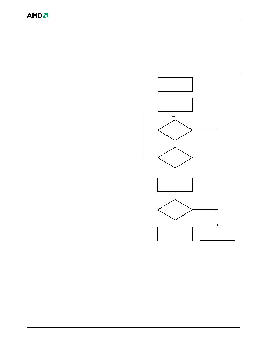
28
Am29DL322D/323D/324D
June 10, 2003
WRITE OPERATION STATUS
The device provides several bits to determine the status of
a program or erase operation: DQ2, DQ3, DQ5, DQ6, and
DQ7. Table 15 and the following subsections describe the
function of these bits. DQ7 and DQ6 each offer a method
for determining whether a program or erase operation is
complete or in progress. The device also provides a hard-
ware-based output signal, RY/BY#, to determine whether
an Embedded Program or Erase operation is in progress or
has been completed.
DQ7: Data# Polling
The Data# Polling bit, DQ7, indicates to the host system
whether an Embedded Program or Erase algorithm is in
progress or completed, or whether a bank is in Erase Sus-
pend. Data# Polling is valid after the rising edge of the final
WE# pulse in the command sequence.
During the Embedded Program algorithm, the device out-
puts on DQ7 the complement of the datum programmed to
DQ7. This DQ7 status also applies to programming during
Erase Suspend. When the Embedded Program algorithm is
complete, the device outputs the datum programmed to
DQ7. The system must provide the program address to
read valid status information on DQ7. If a program address
falls within a protected sector, Data# Polling on DQ7 is ac-
tive for approximately 1 µs, then that bank returns to the
read mode.
During the Embedded Erase algorithm, Data# Polling
produces a "0" on DQ7. When the Embedded Erase
algorithm is complete, or if the bank enters the Erase
Suspend mode, Data# Polling produces a "1" on DQ7.
The system must provide an address within any of the
sectors selected for erasure to read valid status infor-
mation on DQ7.
After an erase command sequence is written, if all
sectors selected for erasing are protected, Data# Poll-
ing on DQ7 is active for approximately 100 µs, then
the bank returns to the read mode. If not all selected
sectors are protected, the Embedded Erase algorithm
erases the unprotected sectors, and ignores the se-
lected sectors that are protected. However, if the sys-
tem reads DQ7 at an address within a protected
sector, the status may not be valid.
Just prior to the completion of an Embedded Program
or Erase operation, DQ7 may change asynchronously
with DQ0≠DQ6 while Output Enable (OE#) is asserted
low. That is, the device may change from providing
status information to valid data on DQ7. Depending on
when the system samples the DQ7 output, it may read
the status or valid data. Even if the device has com-
pleted the program or erase operation and DQ7 has
valid data, the data outputs on DQ0≠DQ6 may be still
invalid. Valid data on DQ0≠DQ7 will appear on suc-
cessive read cycles.
Table 15 shows the outputs for Data# Polling on DQ7.
Figure 5 shows the Data# Polling algorithm. Figure 21
in the AC Characteristics section shows the Data#
Polling timing diagram.
Figure 5. Data# Polling Algorithm
DQ7 = Data?
Yes
No
No
DQ5 = 1?
No
Yes
Yes
FAIL
PASS
Read DQ7≠DQ0
Addr = VA
Read DQ7≠DQ0
Addr = VA
DQ7 = Data?
START
Notes:
1. VA = Valid address for programming. During a sector
erase operation, a valid address is any sector address
within the sector being erased. During chip erase, a
valid address is any non-protected sector address.
2. DQ7 should be rechecked even if DQ5 = "1" because
DQ7 may change simultaneously with DQ5.
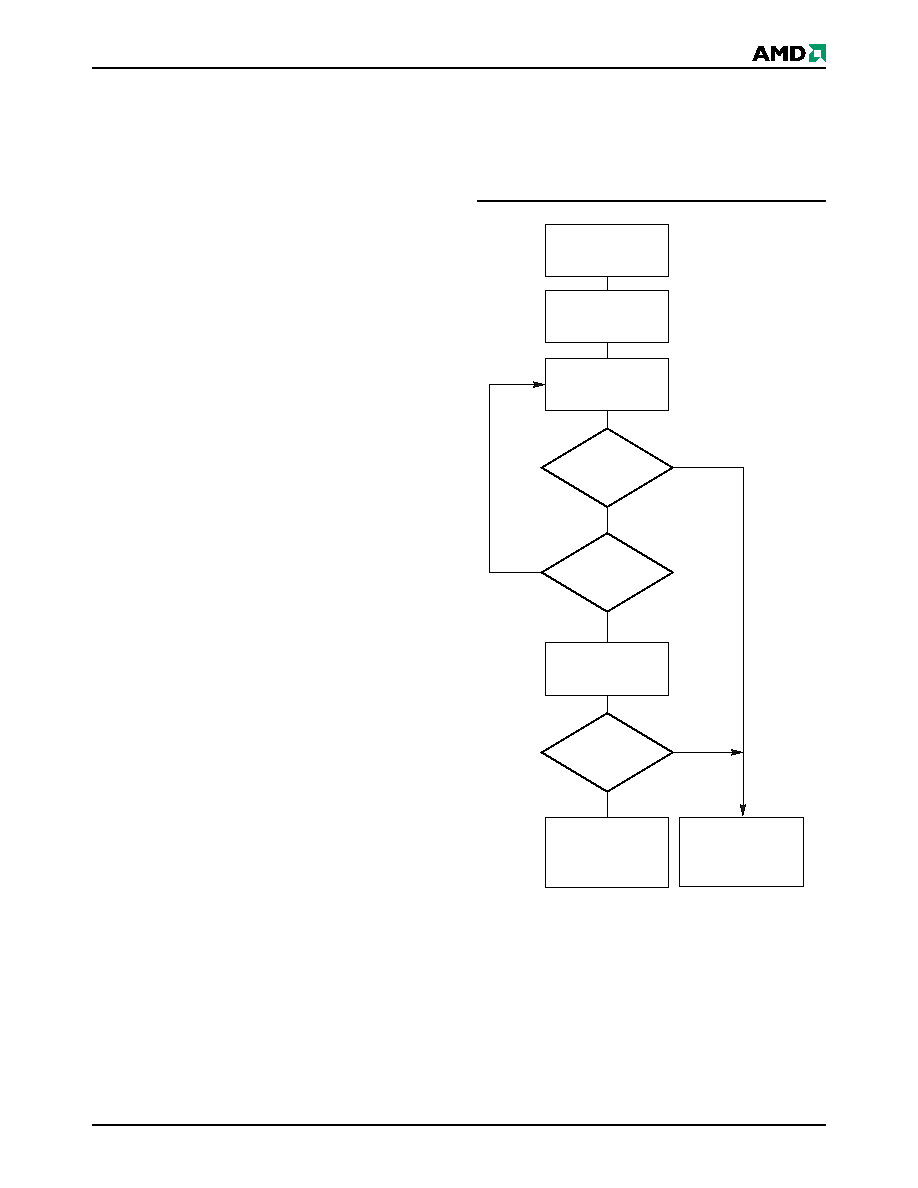
June 10, 2003
Am29DL322D/323D/324D
29
RY/BY#: Ready/Busy#
The RY/BY# is a dedicated, open-drain output pin
which indicates whether an Embedded Algorithm is in
progress or complete. The RY/BY# status is valid after
the rising edge of the final WE# pulse in the command
sequence. Since RY/BY# is an open-drain output, sev-
eral RY/BY# pins can be tied together in parallel with a
pull-up resistor to V
CC
.
If the output is low (Busy), the device is actively eras-
ing or programming. (This includes programming in
the Erase Suspend mode.) If the output is high
(Ready), the device is in the read mode, the standby
mode, or one of the banks is in the erase-sus-
pend-read mode.
Table 15 shows the outputs for RY/BY#.
DQ6: Toggle Bit I
Toggle Bit I on DQ6 indicates whether an Embedded
Program or Erase algorithm is in progress or com-
plete, or whether the device has entered the Erase
Suspend mode. Toggle Bit I may be read at any ad-
dress, and is valid after the rising edge of the final
WE# pulse in the command sequence (prior to the
program or erase operation), and during the sector
erase time-out.
During an Embedded Program or Erase algorithm op-
eration, successive read cycles to any address cause
DQ6 to toggle. The system may use either OE# or
CE# to control the read cycles. When the operation is
complete, DQ6 stops toggling.
After an erase command sequence is written, if all sectors
selected for erasing are protected, DQ6 toggles for approxi-
mately 100 µs, then returns to reading array data. If not all
selected sectors are protected, the Embedded Erase algo-
rithm erases the unprotected sectors, and ignores the se-
lected sectors that are protected.
The system can use DQ6 and DQ2 together to determine
whether a sector is actively erasing or is erase-suspended.
When the device is actively erasing (that is, the Embedded
Erase algorithm is in progress), DQ6 toggles. When the de-
vice enters the Erase Suspend mode, DQ6 stops toggling.
However, the system must also use DQ2 to determine
which sectors are erasing or erase-suspended. Alterna-
tively, the system can use DQ7 (see the subsection on
DQ7: Data# Polling).
If a program address falls within a protected sector,
DQ6 toggles for approximately 1
µ
s after the program
command sequence is written, then returns to reading
array data.
DQ6 also toggles during the erase-suspend-program
mode, and stops toggling once the Embedded Pro-
gram algorithm is complete.
Table 15 shows the outputs for Toggle Bit I on DQ6.
Figure 6 shows the toggle bit algorithm. Figure 22 in
the "AC Characteristics" section shows the toggle bit
timing diagrams. Figure 23 shows the differences be-
tween DQ2 and DQ6 in graphical form. See also the
subsection on DQ2: Toggle Bit II.
Figure 6. Toggle Bit Algorithm
START
No
Yes
Yes
DQ5 = 1?
No
Yes
Toggle Bit
= Toggle?
No
Program/Erase
Operation Not
Complete, Write
Reset Command
Program/Erase
Operation Complete
Read DQ7≠DQ0
Toggle Bit
= Toggle?
Read DQ7≠DQ0
Twice
Read DQ7≠DQ0
Note: The system should recheck the toggle bit even if DQ5
= "1" because the toggle bit may stop toggling as DQ5
changes to "1." See the subsections on DQ6 and DQ2 for
more information.

30
Am29DL322D/323D/324D
June 10, 2003
DQ2: Toggle Bit II
The "Toggle Bit II" on DQ2, when used with DQ6, indi-
cates whether a particular sector is actively erasing
(that is, the Embedded Erase algorithm is in progress),
or whether that sector is erase-suspended. Toggle Bit
II is valid after the rising edge of the final WE# pulse in
the command sequence.
DQ2 toggles when the system reads at addresses
within those sectors that have been selected for era-
sure. (The system may use either OE# or CE# to con-
trol the read cycles.) But DQ2 cannot distinguish
whether the sector is actively erasing or is erase-sus-
pended. DQ6, by comparison, indicates whether the
device is actively erasing, or is in Erase Suspend, but
cannot distinguish which sectors are selected for era-
sure. Thus, both status bits are required for sector and
mode information. Refer to Table 15 to compare out-
puts for DQ2 and DQ6.
Figure 6 shows the toggle bit algorithm in flowchart
form, and the section "DQ2: Toggle Bit II" explains the
algorithm. See also the DQ6: Toggle Bit I subsection.
Figure 22 shows the toggle bit timing diagram. Figure
23 shows the differences between DQ2 and DQ6 in
graphical form.
Reading Toggle Bits DQ6/DQ2
Refer to Figure 6 for the following discussion. When-
ever the system initially begins reading toggle bit sta-
tus, it must read DQ7≠DQ0 at least twice in a row to
determine whether a toggle bit is toggling. Typically,
the system would note and store the value of the tog-
gle bit after the first read. After the second read, the
system would compare the new value of the toggle bit
with the first. If the toggle bit is not toggling, the device
has completed the program or erase operation. The
system can read array data on DQ7≠DQ0 on the fol-
lowing read cycle.
However, if after the initial two read cycles, the system
determines that the toggle bit is still toggling, the sys-
tem also should note whether the value of DQ5 is high
(see the section on DQ5). If it is, the system should
then determine again whether the toggle bit is tog-
gling, since the toggle bit may have stopped toggling
just as DQ5 went high. If the toggle bit is no longer
toggling, the device has successfully completed the
program or erase operation. If it is still toggling, the de-
vice did not completed the operation successfully, and
the system must write the reset command to return to
reading array data.
The remaining scenario is that the system initially de-
termines that the toggle bit is toggling and DQ5 has
not gone high. The system may continue to monitor
the toggle bit and DQ5 through successive read cy-
cles, determining the status as described in the previ-
ous paragraph. Alternatively, it may choose to perform
other system tasks. In this case, the system must start
at the beginning of the algorithm when it returns to de-
termine the status of the operation (top of Figure 6).
DQ5: Exceeded Timing Limits
DQ5 indicates whether the program or erase time has
exceeded a specified internal pulse count limit. Under these
conditions DQ5 produces a "1," indicating that the program
or erase cycle was not successfully completed.
The device may output a "1" on DQ5 if the system tries
to program a "1" to a location that was previously pro-
grammed to "0." Only an erase operation can
change a "0" back to a "1." Under this condition, the
device halts the operation, and when the timing limit
has been exceeded, DQ5 produces a "1."
Under both these conditions, the system must write
the reset command to return to the read mode (or to
the erase-suspend-read mode if a bank was previ-
ously in the erase-suspend-program mode).
DQ3: Sector Erase Timer
After writing a sector erase command sequence, the
system may read DQ3 to determine whether or not
erasure has begun. (The sector erase timer does not
apply to the chip erase command.) If additional
sectors are selected for erasure, the entire time-out
also applies after each additional sector erase com-
mand. When the time-out period is complete, DQ3
switches from a "0" to a "1." If the time between addi-
tional sector erase commands from the system can be
assumed to be less than 50 µs, the system need not
monitor DQ3. See also the Sector Erase Command
Sequence section.
After the sector erase command is written, the system
should read the status of DQ7 (Data# Polling) or DQ6
(Toggle Bit I) to ensure that the device has accepted
the command sequence, and then read DQ3. If DQ3 is
"1," the Embedded Erase algorithm has begun; all fur-
ther commands (except Erase Suspend) are ignored
until the erase operation is complete. If DQ3 is "0," the
device will accept additional sector erase commands.
To ensure the command has been accepted, the sys-
tem software should check the status of DQ3 prior to
and following each subsequent sector erase com-
mand. If DQ3 is high on the second status check, the
last command might not have been accepted.
Table 15 shows the status of DQ3 relative to the other
status bits.
June 10, 2003
Am29DL322D/323D/324D
31
Table 15. Write Operation Status
Notes:
1. DQ5 switches to `1' when an Embedded Program or Embedded Erase operation has exceeded the maximum timing limits.
Refer to the section on DQ5 for more information.
2. DQ7 and DQ2 require a valid address when reading status information. Refer to the appropriate subsection for further
details.
3. When reading write operation status bits, the system must always provide the bank address where the Embedded Algorithm
is in progress. The device outputs array data if the system addresses a non-busy bank.
Status
DQ7
(Note 2)
DQ6
DQ5
(Note 1)
DQ3
DQ2
(Note 2)
RY/BY#
Standard
Mode
Embedded Program Algorithm
DQ7#
Toggle
0
N/A
No toggle
0
Embedded Erase Algorithm
0
Toggle
0
1
Toggle
0
Erase
Suspend
Mode
Erase-Suspend-
Read
Erase
Suspended Sector
1
No toggle
0
N/A
Toggle
1
Non-Erase
Suspended Sector
Data
Data
Data
Data
Data
1
Erase-Suspend-Program
DQ7#
Toggle
0
N/A
N/A
0
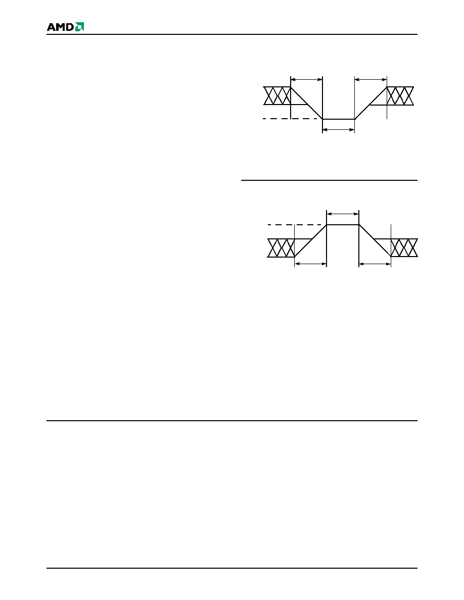
32
Am29DL322D/323D/324D
June 10, 2003
ABSOLUTE MAXIMUM RATINGS
Storage Temperature
Plastic Packages . . . . . . . . . . . . . . . ≠65
∞
C to +150
∞
C
Ambient Temperature
with Power Applied . . . . . . . . . . . . . ≠65
∞
C to +125
∞
C
Voltage with Respect to Ground
V
CC
(Note 1) . . . . . . . . . . . . . . . . .≠0.5 V to +4.0 V
A9, OE#, and RESET#
(Note 2). . . . . . . . . . . . . . . . . . . .≠0.5 V to +12.5 V
WP#/ACC . . . . . . . . . . . . . . . . . .≠0.5 V to +10.5 V
All other pins (Note 1) . . . . . . ≠0.5 V to V
CC
+0.5 V
Output Short Circuit Current (Note 3) . . . . . . 200 mA
Notes:
1. Minimum DC voltage on input or I/O pins is ≠0.5 V.
During voltage transitions, input or I/O pins may
overshoot V
SS
to ≠2.0 V for periods of up to 20 ns.
Maximum DC voltage on input or I/O pins is V
CC
+0.5 V.
See Figure 7. During voltage transitions, input or I/O pins
may overshoot to V
CC
+2.0 V for periods up to 20 ns. See
Figure 8.
2. Minimum DC input voltage on pins A9, OE#, RESET#,
and WP#/ACC is ≠0.5 V. During voltage transitions, A9,
OE#, WP#/ACC, and RESET# may overshoot V
SS
to
≠2.0 V for periods of up to 20 ns. See Figure 7. Maximum
DC input voltage on pin A9 is +12.5 V which may
overshoot to +14.0 V for periods up to 20 ns. Maximum
DC input voltage on WP#/ACC is +9.5 V which may
overshoot to +12.0 V for periods up to 20 ns.
3. No more than one output may be shorted to ground at a
time. Duration of the short circuit should not be greater
than one second.
Stresses above those listed under "Absolute Maximum
Ratings" may cause permanent damage to the device. This
is a stress rating only; functional operation of the device at
these or any other conditions above those indicated in the
operational sections of this data sheet is not implied.
Exposure of the device to absolute maximum rating
conditions for extended periods may affect device reliability.
Figure 7. Maximum Negative
Overshoot Waveform
Figure 8. Maximum Positive
Overshoot Waveform
OPERATING RANGES
Industrial (I) Devices
Ambient Temperature (T
A
) . . . . . . . . . ≠40∞C to +85∞C
Extended (E) Devices
Ambient Temperature (T
A
) . . . . . . . . ≠55∞C to +125∞C
V
CC
Supply Voltages
V
CC
for regulated voltage range . . . . . . . 3.0 V to 3.6 V
V
CC
for standard voltage range . . . . . . . 2.7 V to 3.6 V
Operating ranges define those limits between which the
functionality of the device is guaranteed.
20 ns
20 ns
+0.8 V
≠0.5 V
20 ns
≠2.0 V
20 ns
20 ns
V
CC
+2.0 V
V
CC
+0.5 V
20 ns
2.0 V
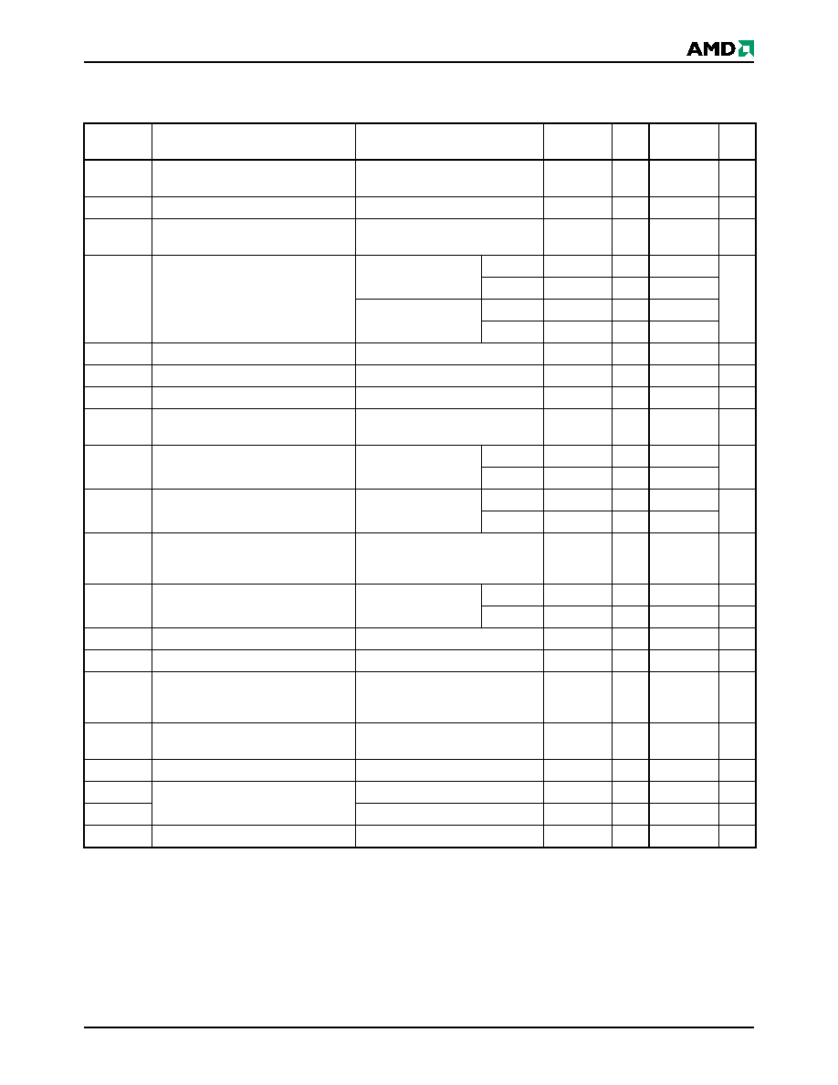
June 10, 2003
Am29DL322D/323D/324D
33
DC CHARACTERISTICS
CMOS Compatible
Notes:
1. The I
CC
current listed is typically less than 2 mA/MHz, with OE# at V
IH
.
2. Maximum I
CC
specifications are tested with V
CC
= V
CC
max.
3. I
CC
active while Embedded Erase or Embedded Program is in progress.
4. Automatic sleep mode enables the low power mode when addresses remain stable for t
ACC
+ 30 ns. Typical sleep mode current is
200 nA.
5. Not 100% tested.
Parameter
Symbol
Parameter Description
Test Conditions
Min
Typ
Max
Unit
I
LI
Input Load Current
V
IN
= V
SS
to V
CC
,
V
CC
= V
CC
max
±
1.0
µA
I
LIT
A9 Input Load Current
V
CC
= V
CC max
; A9 = 12.5 V
35
µA
I
LO
Output Leakage Current
V
OUT
= V
SS
to V
CC
,
V
CC
= V
CC max
±
1.0
µA
I
CC1
V
CC
Active Read Current
(Notes 1, 2)
CE# = V
IL,
OE#
=
V
IH
,
Byte Mode
5 MHz
10
16
mA
1 MHz
2
4
CE# = V
IL,
OE#
=
V
IH
,
Word Mode
5 MHz
10
16
1 MHz
2
4
I
CC2
V
CC
Active Write Current (Notes 2, 3) CE# = V
IL,
OE#
=
V
IH
, WE# = V
IL
15
30
mA
I
CC3
V
CC
Standby Current (Note 2)
CE#, RESET# = V
CC
±
0.3 V
0.2
5
µA
I
CC4
V
CC
Reset Current (Note 2)
RESET# = V
SS
±
0.3 V
0.2
5
µA
I
CC5
Automatic Sleep Mode (Notes 2, 4)
V
IH
= V
CC
±
0.3 V;
V
IL
= V
SS
±
0.3 V
0.2
5
µA
I
CC6
V
CC
Active Read-While-Program
Current (Notes 1, 2)
CE# = V
IL
,
OE# = V
IH
Byte
21
45
mA
Word
21
45
I
CC7
V
CC
Active Read-While-Erase
Current (Notes 1, 2)
CE# = V
IL
, OE# = V
IH
Byte
21
45
mA
Word
21
45
I
CC8
V
CC
Active
Program-While-Erase-Suspended
Current (Notes 2, 5)
CE# = V
IL
, OE# = V
IH
17
35
mA
I
ACC
ACC Accelerated Program Current,
Word or Byte
CE# = V
IL
, OE# = V
IH
ACC pin
5
10
mA
V
CC
pin
15
30
mA
V
IL
Input Low Voltage
≠0.5
0.8
V
V
IH
Input High Voltage
0.7 x V
CC
V
CC
+ 0.3
V
V
HH
Voltage for WP#/ACC Sector
Protect/Unprotect and Program
Acceleration
V
CC
= 3.0 V ± 10%
8.5
9.5
V
V
ID
Voltage for Autoselect and
Temporary Sector Unprotect
V
CC
= 3.0 V
±
10%
8.5
12.5
V
V
OL
Output Low Voltage
I
OL
= 4.0 mA, V
CC
= V
CC min
0.45
V
V
OH1
Output High Voltage
I
OH
= ≠2.0 mA, V
CC
= V
CC min
0.85
V
CC
V
V
OH2
I
OH
= ≠100 µA, V
CC
= V
CC min
V
CC
≠0.4
V
LKO
Low V
CC
Lock-Out Voltage (Note 5)
2.3
2.5
V
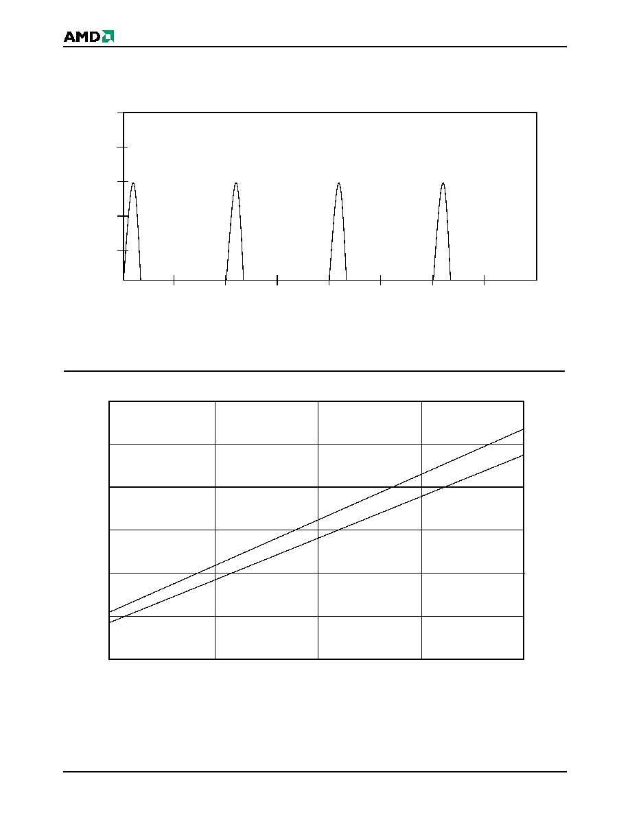
34
Am29DL322D/323D/324D
June 10, 2003
DC CHARACTERISTICS
Zero-Power Flash
Note: Addresses are switching at 1 MHz
Figure 9. I
CC1
Current vs. Time (Showing Active and Automatic Sleep Currents)
25
20
15
10
5
0
0
500
1000
1500
2000
2500
3000
3500
4000
Su
pply
Curre
nt in
mA
Time in ns
10
8
2
0
1
2
3
4
5
Frequency in MHz
Supply Current in mA
Note: T = 25
∞
C
Figure 10. Typical I
CC1
vs. Frequency
2.7 V
3.6 V
4
6
12
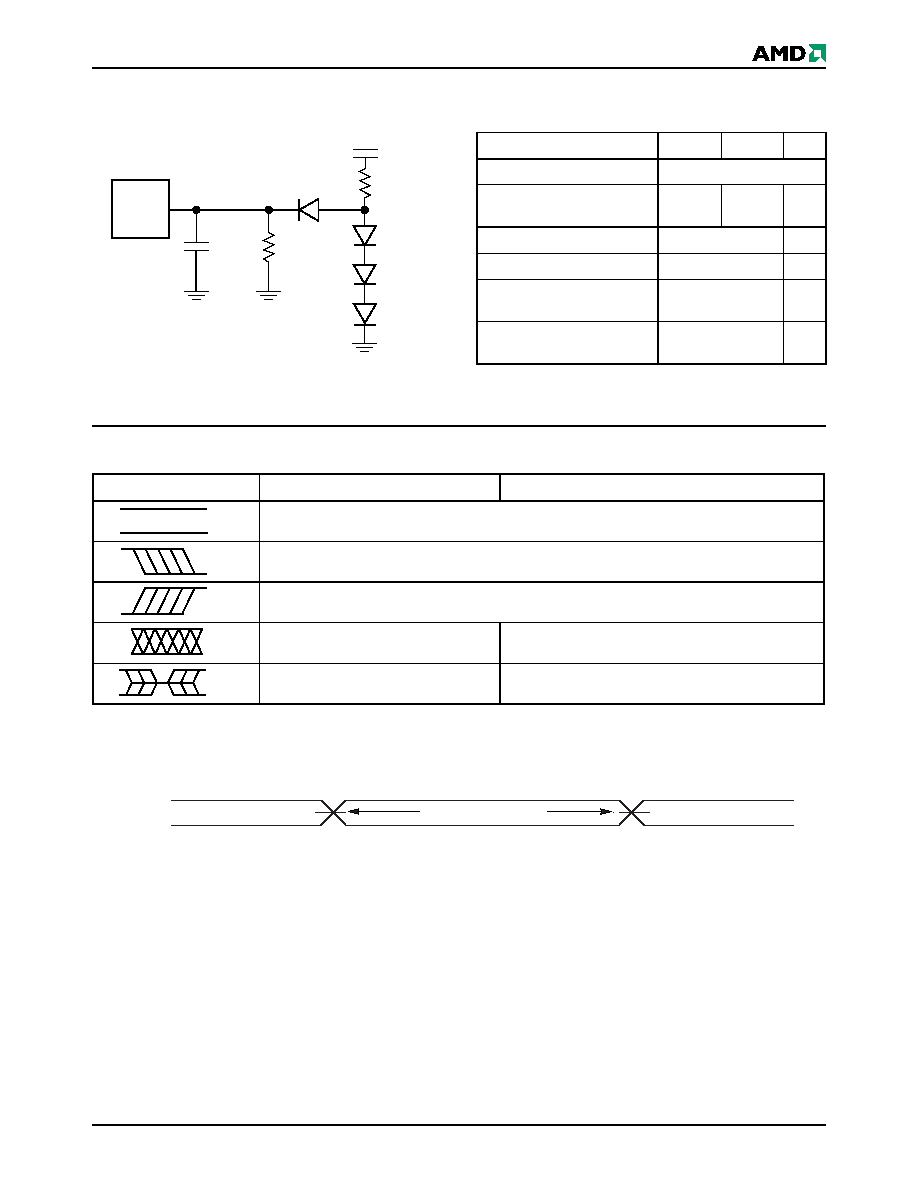
June 10, 2003
Am29DL322D/323D/324D
35
TEST CONDITIONS
Table 16. Test Specifications
KEY TO SWITCHING WAVEFORMS
2.7 k
C
L
6.2 k
3.3 V
Device
Under
Test
Note: Diodes are IN3064 or equivalent
Figure 11. Test Setup
Test Condition
70R, 90
120
Unit
Output Load
1 TTL gate
Output Load Capacitance, C
L
(including jig capacitance)
30
100
pF
Input Rise and Fall Times
5
ns
Input Pulse Levels
0.0≠3.0
V
Input timing measurement
reference levels
1.5 V
Output timing measurement
reference levels
1.5
V
WAVEFORM
INPUTS
OUTPUTS
Steady
Changing from H to L
Changing from L to H
Don't Care, Any Change Permitted
Changing, State Unknown
Does Not Apply
Center Line is High Impedance State (High Z)
3.0 V
0.0 V
1.5 V
1.5 V
Output
Measurement Level
Input
Figure 12. Input Waveforms and Measurement Levels
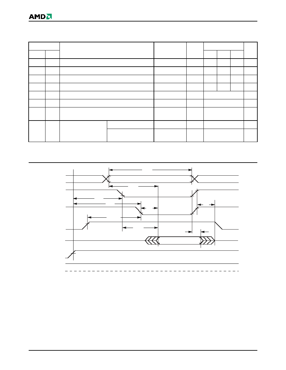
36
Am29DL322D/323D/324D
June 10, 2003
AC CHARACTERISTICS
Read-Only Operations
Notes:
1. Not 100% tested.
2. See Figure 11 and Table 16 for test specifications.
Parameter
Description
Test Setup
Speed Options
JEDEC
Std.
70R
90
120
Unit
t
AVAV
t
RC
Read Cycle Time (Note 1)
Min
70
90
120
ns
t
AVQV
t
ACC
Address to Output Delay
CE#, OE# = V
IL
Max
70
90
120
ns
t
ELQV
t
CE
Chip Enable to Output Delay
OE# = V
IL
Max
70
90
120
ns
t
GLQV
t
OE
Output Enable to Output Delay
Max
30
40
50
ns
t
EHQZ
t
DF
Chip Enable to Output High Z (Note 1)
Max
16
ns
t
GHQZ
t
DF
Output Enable to Output High Z (Note 1)
Max
16
ns
t
AXQX
t
OH
Output Hold Time From Addresses, CE# or OE#,
Whichever Occurs First
Min
0
ns
t
OEH
Output Enable Hold Time
(Note 1)
Read
Min
0
ns
Toggle and
Data# Polling
Min
10
ns
t
OH
t
CE
Outputs
WE#
Addresses
CE#
OE#
HIGH Z
Output Valid
HIGH Z
Addresses Stable
t
RC
t
ACC
t
OEH
t
RH
t
OE
t
RH
0 V
RY/BY#
RESET#
t
DF
Figure 13. Read Operation Timings
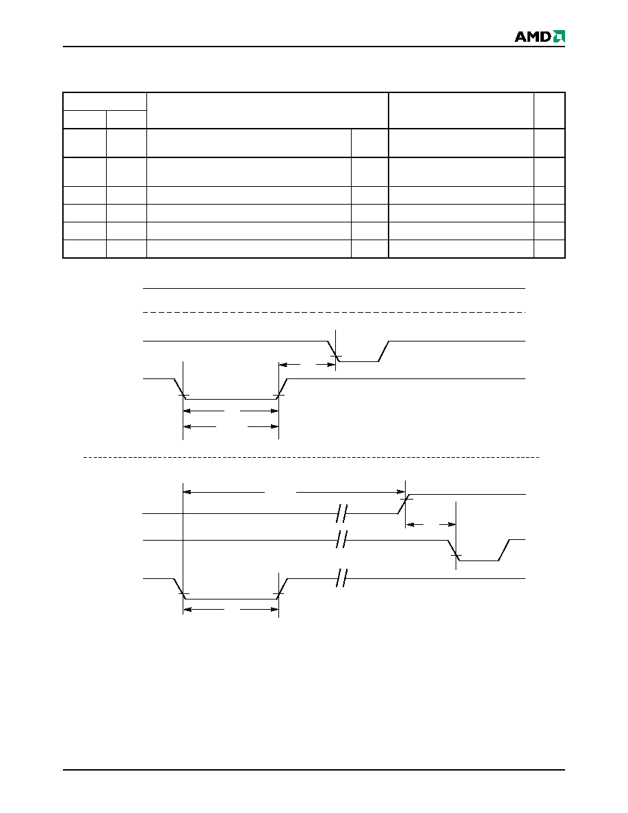
June 10, 2003
Am29DL322D/323D/324D
37
AC CHARACTERISTICS
Hardware Reset (RESET#)
Note: Not 100% tested.
Parameter
Description
All Speed Options
Unit
JEDEC
Std
t
Ready
RESET# Pin Low (During Embedded Algorithms)
to Read Mode (See Note)
Max
20
µ
s
t
Ready
RESET# Pin Low (NOT During Embedded
Algorithms) to Read Mode (See Note)
Max
500
ns
t
RP
RESET# Pulse Width
Min
500
ns
t
RH
Reset High Time Before Read (See Note)
Min
50
ns
t
RPD
RESET# Low to Standby Mode
Min
20
µ
s
t
RB
RY/BY# Recovery Time
Min
0
ns
RESET#
RY/BY#
RY/BY#
t
RP
t
Ready
Reset Timings NOT during Embedded Algorithms
t
Ready
CE#, OE#
t
RH
CE#, OE#
Reset Timings during Embedded Algorithms
RESET#
t
RP
t
RB
Figure 14. Reset Timings
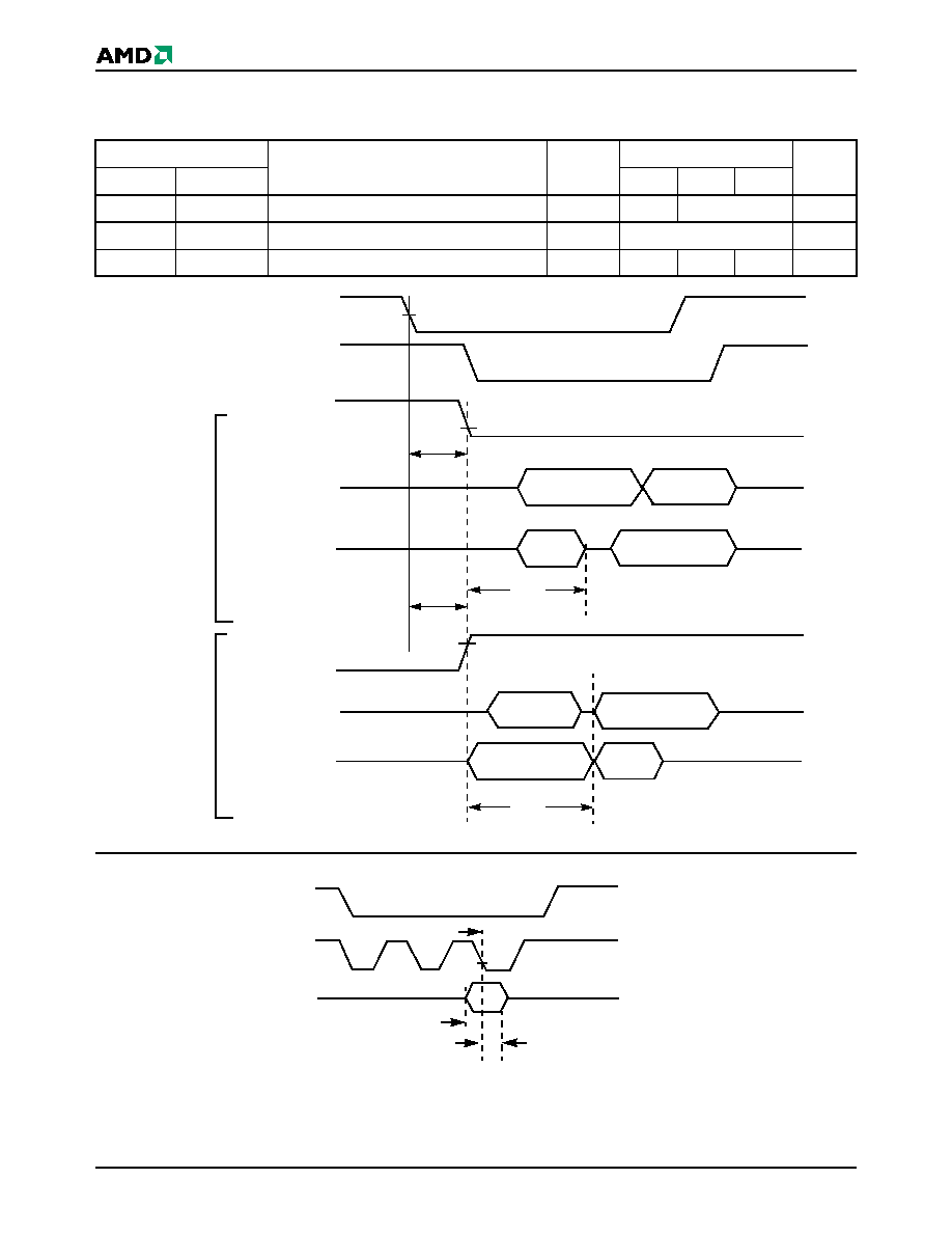
38
Am29DL322D/323D/324D
June 10, 2003
AC CHARACTERISTICS
Word/Byte Configuration (BYTE#)
Parameter
Speed Options
JEDEC
Std
Description
70R
90
120
Unit
t
ELFL
/t
ELFH
CE# to BYTE# Switching Low or High
Max
70
5
ns
t
FLQZ
BYTE# Switching Low to Output HIGH Z
Max
16
ns
t
FHQV
BYTE# Switching High to Output Active
Min
70
90
120
ns
DQ15
Output
Data Output
(DQ0≠DQ7)
CE#
OE#
BYTE#
t
ELFL
DQ0≠DQ14
Data Output
(DQ0≠DQ14)
DQ15/A-1
Address
Input
t
FLQZ
BYTE#
Switching
from word
to byte
mode
DQ15
Output
Data Output
(DQ0≠DQ7)
BYTE#
t
ELFH
DQ0≠DQ14
Data Output
(DQ0≠DQ14)
DQ15/A-1
Address
Input
t
FHQV
BYTE#
Switching
from byte
to word
mode
Figure 15. BYTE# Timings for Read Operations
Note: Refer to the Erase/Program Operations table for t
AS
and t
AH
specifications.
Figure 16. BYTE# Timings for Write Operations
CE#
WE#
BYTE#
The falling edge of the last WE# signal
t
HOLD
(t
AH
)
t
SET
(t
AS
)
June 10, 2003
Am29DL322D/323D/324D
39
AC CHARACTERISTICS
Erase and Program Operations
Notes:
1. Not 100% tested.
2. See the "Erase And Programming Performance" section for more information.
Parameter
Speed Options
JEDEC
Std
Description
70R
90
120
Unit
t
AVAV
t
WC
Write Cycle Time (Note 1)
Min
70
90
120
ns
t
AVWL
t
AS
Address Setup Time
Min
0
ns
t
ASO
Address Setup Time to OE# low during toggle bit polling
Min
15
15
ns
t
WLAX
t
AH
Address Hold Time
Min
45
45
50
ns
t
AHT
Address Hold Time From CE# or OE# high
during toggle bit polling
Min
0
ns
t
DVWH
t
DS
Data Setup Time
Min
35
45
50
ns
t
WHDX
t
DH
Data Hold Time
Min
0
ns
t
OEPH
Output Enable High during toggle bit polling
Min
20
ns
t
GHWL
t
GHWL
Read Recovery Time Before Write
(OE# High to WE# Low)
Min
0
ns
t
ELWL
t
CS
CE# Setup Time
Min
0
ns
t
WHEH
t
CH
CE# Hold Time
Min
0
ns
t
WLWH
t
WP
Write Pulse Width
Min
30
35
50
ns
t
WHDL
t
WPH
Write Pulse Width High
Min
30
ns
t
SR/W
Latency Between Read and Write Operations
Min
0
ns
t
WHWH1
t
WHWH1
Programming Operation (Note 2)
Byte
Typ
5
µs
Word
Typ
7
t
WHWH1
t
WHWH1
Accelerated Programming Operation,
Word or Byte (Note 2)
Typ
4
µs
t
WHWH2
t
WHWH2
Sector Erase Operation (Note 2)
Typ
0.7
sec
t
VCS
V
CC
Setup Time (Note 1)
Min
50
µs
t
RB
Write Recovery Time from RY/BY#
Min
0
ns
t
BUSY
Program/Erase Valid to RY/BY# Delay
Min
90
ns
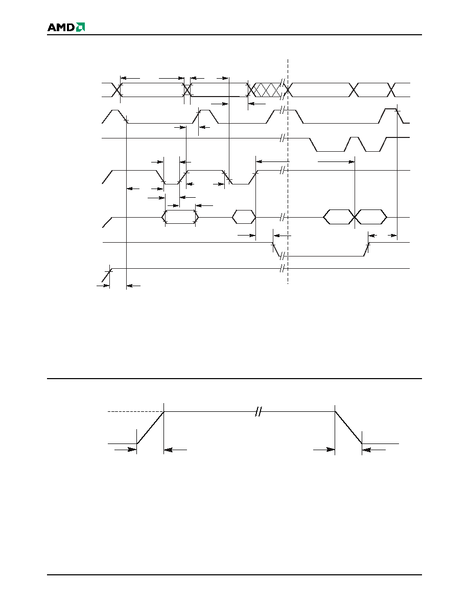
40
Am29DL322D/323D/324D
June 10, 2003
AC CHARACTERISTICS
OE#
WE#
CE#
V
CC
Data
Addresses
t
DS
t
AH
t
DH
t
WP
PD
t
WHWH1
t
WC
t
AS
t
WPH
t
VCS
555h
PA
PA
Read Status Data (last two cycles)
A0h
t
CS
Status
D
OUT
Program Command Sequence (last two cycles)
RY/BY#
t
RB
t
BUSY
t
CH
PA
Notes:
1. PA = program address, PD = program data, D
OUT
is the true data at the program address.
2. Illustration shows device in word mode.
Figure 17. Program Operation Timings
WP#/ACC
t
VHH
V
HH
V
IL
or V
IH
V
IL
or V
IH
t
VHH
Figure 18. Accelerated Program Timing Diagram
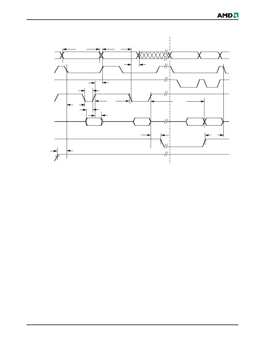
June 10, 2003
Am29DL322D/323D/324D
41
AC CHARACTERISTICS
OE#
CE#
Addresses
V
CC
WE#
Data
2AAh
SA
t
AH
t
WP
t
WC
t
AS
t
WPH
555h for chip erase
10 for Chip Erase
30h
t
DS
t
VCS
t
CS
t
DH
55h
t
CH
In
Progress
Complete
t
WHWH2
VA
VA
Erase Command Sequence (last two cycles)
Read Status Data
RY/BY#
t
RB
t
BUSY
Notes:
1. SA = sector address (for Sector Erase), VA = Valid Address for reading status data (see "Write Operation Status".
2. These waveforms are for the word mode.
Figure 19. Chip/Sector Erase Operation Timings
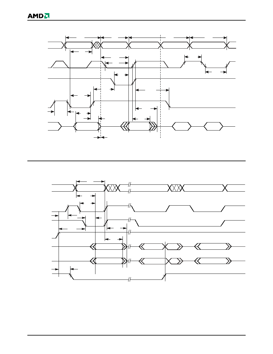
42
Am29DL322D/323D/324D
June 10, 2003
AC CHARACTERISTICS
OE#
CE#
WE#
Addresses
t
OH
Data
Valid
In
Valid
In
Valid PA
Valid RA
t
WC
t
WPH
t
AH
t
WP
t
DS
t
DH
t
RC
t
CE
Valid
Out
t
OE
t
ACC
t
OEH
t
GHWL
t
DF
Valid
In
CE# Controlled Write Cycles
WE# Controlled Write Cycle
Valid PA
Valid PA
t
CP
t
CPH
t
WC
t
WC
Read Cycle
t
SR/W
Figure 20. Back-to-back Read/Write Cycle Timings
WE#
CE#
OE#
High Z
t
OE
High Z
DQ7
DQ0≠DQ6
RY/BY#
t
BUSY
Complement
True
Addresses
VA
t
OEH
t
CE
t
CH
t
OH
t
DF
VA
VA
Status Data
Complement
Status Data
True
Valid Data
Valid Data
t
ACC
t
RC
Note: VA = Valid address. Illustration shows first status cycle after command sequence, last status read cycle, and array data
read cycle.
Figure 21. Data# Polling Timings (During Embedded Algorithms)
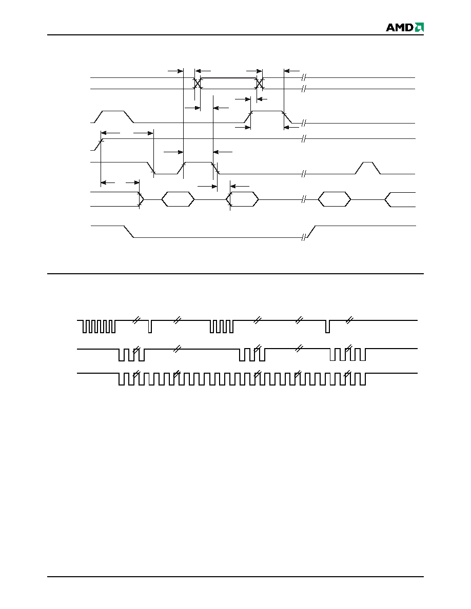
June 10, 2003
Am29DL322D/323D/324D
43
AC CHARACTERISTICS
OE#
CE#
WE#
Addresses
t
OEH
t
DH
t
AHT
t
ASO
t
OEPH
t
OE
Valid Data
(first read)
(second read)
(stops toggling)
t
CEPH
t
AHT
t
AS
DQ6/DQ2
Valid Data
Valid
Status
Valid
Status
Valid
Status
RY/BY#
Note: VA = Valid address; not required for DQ6. Illustration shows first two status cycle after command sequence, last status
read cycle, and array data read cycle
Figure 22. Toggle Bit Timings (During Embedded Algorithms)
Note: DQ2 toggles only when read at an address within an erase-suspended sector. The system may use OE# or CE# to toggle
DQ2 and DQ6.
Figure 23. DQ2 vs. DQ6
Enter
Erase
Erase
Erase
Enter Erase
Suspend Program
Erase Suspend
Read
Erase Suspend
Read
Erase
WE#
DQ6
DQ2
Erase
Complete
Erase
Suspend
Suspend
Program
Resume
Embedded
Erasing
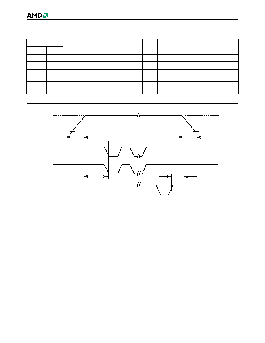
44
Am29DL322D/323D/324D
June 10, 2003
AC CHARACTERISTICS
Temporary Sector Unprotect
Note: Not 100% tested.
Parameter
All Speed Options
JEDEC
Std
Description
Unit
t
VIDR
V
ID
Rise and Fall Time (See Note)
Min
500
ns
t
VHH
V
HH
Rise and Fall Time (See Note)
Min
250
ns
t
RSP
RESET# Setup Time for Temporary Sector
Unprotect
Min
4
µ
s
t
RRB
RESET# Hold Time from RY/BY# High for
Temporary Sector Unprotect
Min
4
µ
s
RESET#
t
VIDR
V
ID
V
SS
, V
IL
,
or V
IH
V
ID
V
SS
, V
IL
,
or V
IH
CE#
WE#
RY/BY#
t
VIDR
t
RSP
Program or Erase Command Sequence
t
RRB
Figure 24. Temporary Sector Unprotect Timing Diagram
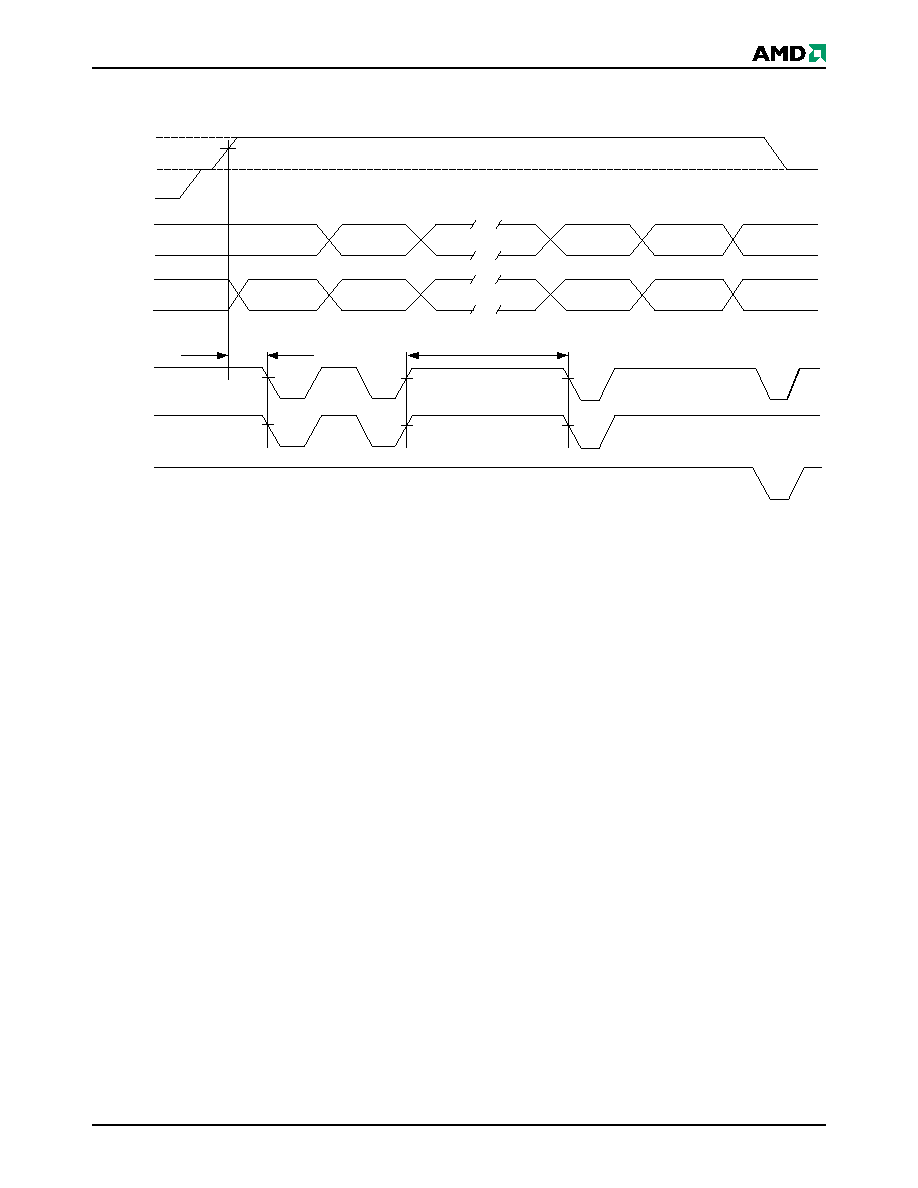
June 10, 2003
Am29DL322D/323D/324D
45
AC CHARACTERISTICS
Sector/Sector Block Protect: 150 µs,
Sector/Sector Block Unprotect: 15 ms
1 µs
RESET#
SA, A6,
A1, A0
Data
CE#
WE#
OE#
60h
60h
40h
Valid*
Valid*
Valid*
Status
Sector/Sector Block Protect or Unprotect
Verify
V
ID
V
IH
* For sector protect, A6 = 0, A1 = 1, A0 = 0. For sector unprotect, A6 = 1, A1 = 1, A0 = 0.
Figure 25. Sector/Sector Block Protect and Unprotect Timing Diagram
46
Am29DL322D/323D/324D
June 10, 2003
AC CHARACTERISTICS
Alternate CE# Controlled Erase and Program Operations
Notes:
1. Not 100% tested.
2. See the "Erase And Programming Performance" section for more information.
Parameter
Speed Options
JEDEC
Std
Description
70R
90
120
Unit
t
AVAV
t
WC
Write Cycle Time (Note 1)
Min
70
90
120
ns
t
AVWL
t
AS
Address Setup Time
Min
0
ns
t
ELAX
t
AH
Address Hold Time
Min
45
45
50
ns
t
DVEH
t
DS
Data Setup Time
Min
45
45
50
ns
t
EHDX
t
DH
Data Hold Time
Min
0
ns
t
GHEL
t
GHEL
Read Recovery Time Before Write
(OE# High to WE# Low)
Min
0
ns
t
WLEL
t
WS
WE# Setup Time
Min
0
ns
t
EHWH
t
WH
WE# Hold Time
Min
0
ns
t
ELEH
t
CP
CE# Pulse Width
Min
45
45
50
ns
t
EHEL
t
CPH
CE# Pulse Width High
Min
30
ns
t
WHWH1
t
WHWH1
Programming Operation
(Note 2)
Byte
Typ
5
µs
Word
Typ
7
t
WHWH1
t
WHWH1
Accelerated Programming Operation,
Word or Byte (Note 2)
Typ
4
µs
t
WHWH2
t
WHWH2
Sector Erase Operation (Note 2)
Typ
0.7
sec
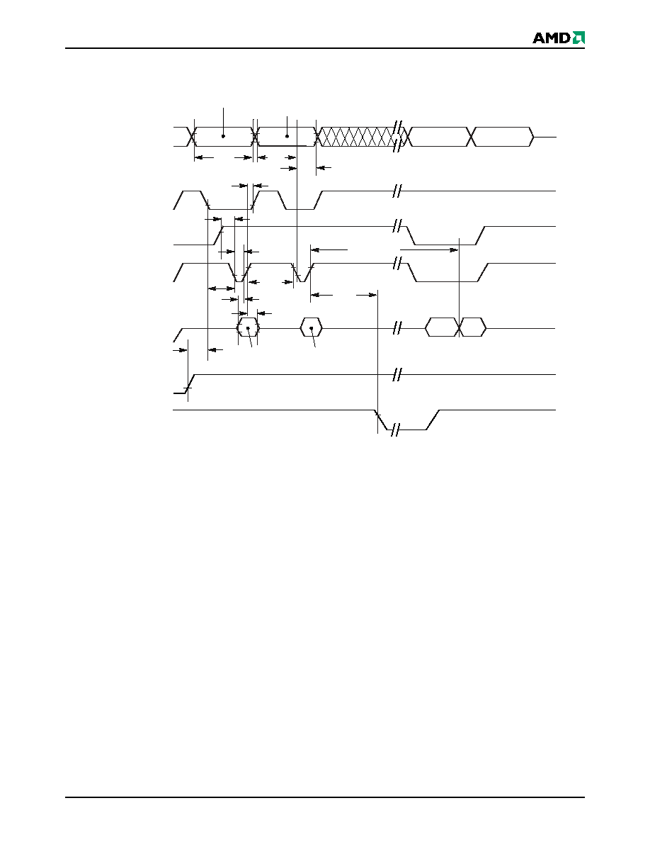
June 10, 2003
Am29DL322D/323D/324D
47
AC CHARACTERISTICS
t
GHEL
t
WS
OE#
CE#
WE#
RESET#
t
DS
Data
t
AH
Addresses
t
DH
t
CP
DQ7#
D
OUT
t
WC
t
AS
t
CPH
PA
Data# Polling
A0 for program
55 for erase
t
RH
t
WHWH1 or 2
RY/BY#
t
WH
PD for program
30 for sector erase
10 for chip erase
555 for program
2AA for erase
PA for program
SA for sector erase
555 for chip erase
t
BUSY
Notes:
1. Figure indicates last two bus cycles of a program or erase operation.
2. PA = program address, SA = sector address, PD = program data.
3. DQ7# is the complement of the data written to the device. D
OUT
is the data written to the device.
4. Waveforms are for the word mode.
Figure 26. Alternate CE# Controlled Write (Erase/Program) Operation Timings
48
Am29DL322D/323D/324D
June 10, 2003
ERASE AND PROGRAMMING PERFORMANCE
Notes:
1. Typical program and erase times assume the following conditions: 25
∞
C, 3.0 V V
CC
, 1,000,000 cycles. Additionally,
programming typicals assume checkerboard pattern.
2. Under worst case conditions of 90
∞
C, V
CC
= 2.7 V (3.0 V for regulated devices), 1,000,000 cycles.
3. The typical chip programming time is considerably less than the maximum chip programming time listed, since most bytes
program faster than the maximum program times listed.
4. In the pre-programming step of the Embedded Erase algorithm, all bytes are programmed to 00h before erasure.
5. System-level overhead is the time required to execute the two- or four-bus-cycle sequence for the program command. See Table
14 for further information on command definitions.
6. The device has a minimum erase and program cycle endurance of 1,000,000 cycles.
LATCHUP CHARACTERISTICS
Note: Includes all pins except V
CC
. Test conditions: V
CC
= 3.0 V, one pin at a time.
TSOP AND SO PIN CAPACITANCE
Notes:
1. Sampled, not 100% tested.
2. Test conditions T
A
= 25∞C, f = 1.0 MHz.
DATA RETENTION
Parameter
Typ (Note 1)
Max (Note 2)
Unit
Comments
Sector Erase Time
0.7
15
sec
Excludes 00h programming
prior to erasure (Note 4)
Chip Erase Time
49
sec
Byte Program Time
5
150
µs
Excludes system level
overhead (Note 5)
Accelerated Byte/Word Program Time
4
120
µs
Word Program Time
7
210
µs
Chip Program Time
(Note 3)
Byte Mode
21
63
sec
Word Mode
14
42
Description
Min
Max
Input voltage with respect to V
SS
on all pins except I/O pins
(including A9, OE#, and RESET#)
≠1.0 V
12.5 V
Input voltage with respect to V
SS
on all I/O pins
≠1.0 V
V
CC
+ 1.0 V
V
CC
Current
≠100 mA
+100 mA
Parameter
Symbol
Parameter Description
Test Setup
Typ
Max
Unit
C
IN
Input Capacitance
V
IN
= 0
6
7.5
pF
C
OUT
Output Capacitance
V
OUT
= 0
8.5
12
pF
C
IN2
Control Pin Capacitance
V
IN
= 0
7.5
9
pF
Parameter Description
Test Conditions
Min
Unit
Minimum Pattern Data Retention Time
150
∞
C
10
Years
125
∞
C
20
Years
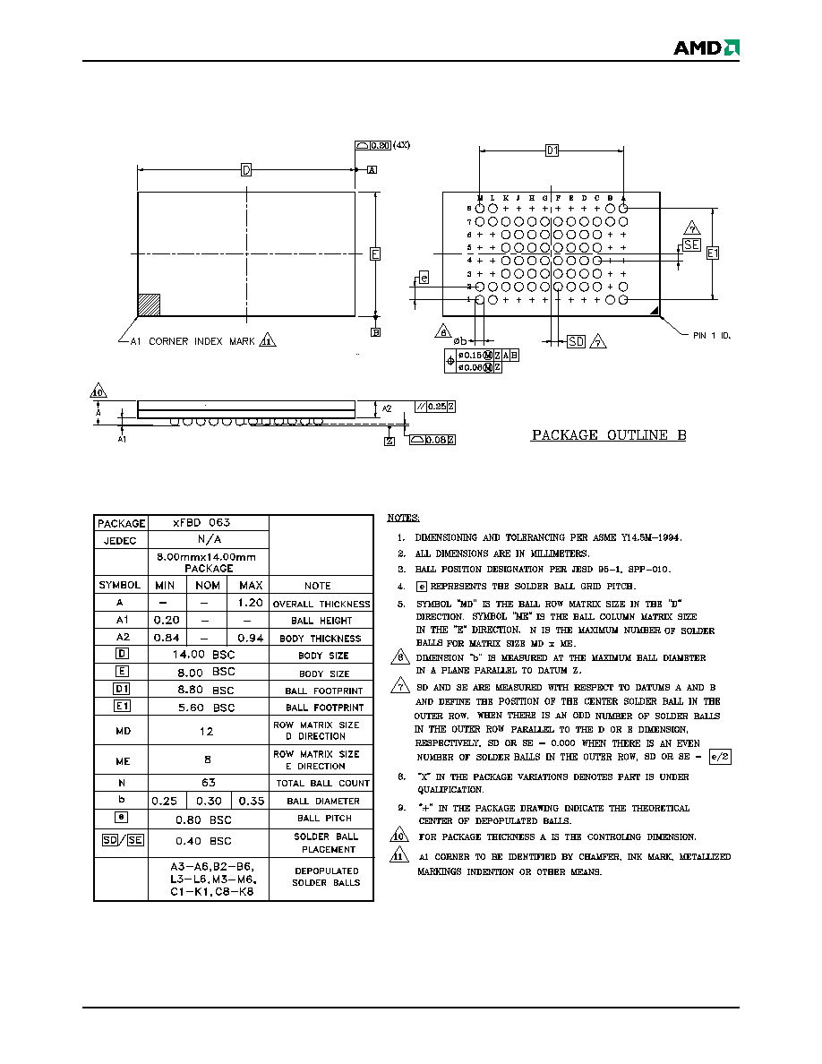
June 10, 2003
Am29DL322D/323D/324D
49
PHYSICAL DIMENSIONS
FBD063--63-ball Fine-Pitch Ball Grid Array (FBGA) 8 x 14 mm
Dwg rev AF; 10/99
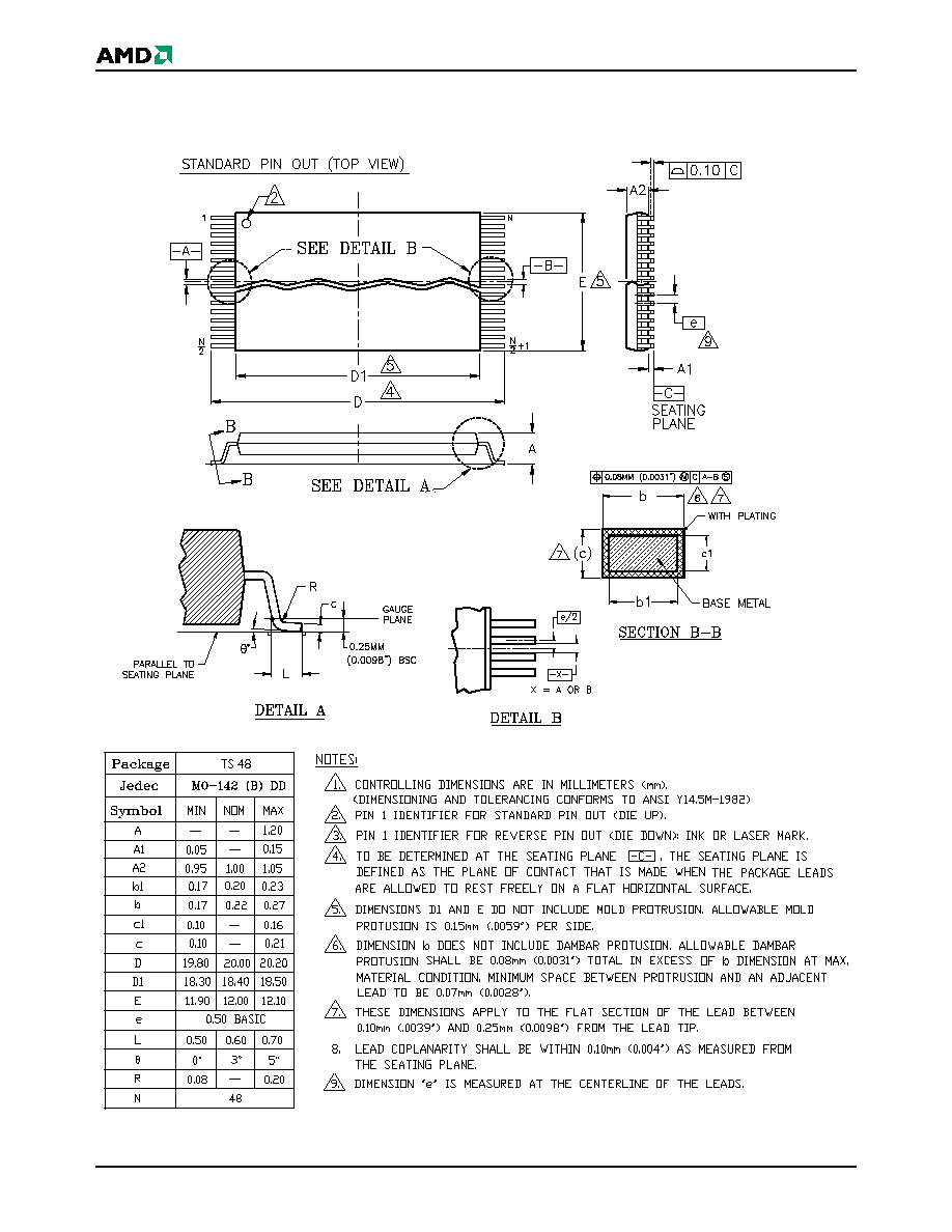
50
Am29DL322D/323D/324D
June 10, 2003
PHYSICAL DIMENSIONS
TS 048--48-Pin Standard TSOP
Dwg rev AA; 10/99

June 10, 2003
Am29DL322D/323D/324D
51
REVISION SUMMARY
Revision B (October 1998)
Global
Deleted the 90R and 120R speed options. Expanded
the full voltage range to 2.7≠3.6 V.
Distinctive Characteristics
Added 125
∞
C to 20-year data retention bullet.
Connection Diagrams
Changed the FBGA diagram from bottom view to
top view.
Ordering Information
Changed the FBGA ordering nomenclature to "YD."
The package designation is now FBD063.
Device Bus Operations
Accelerated Program Operation and Write Protect
(WP#) sections: Added note to indicate that the
WP#/ACC must not be left floating or unconnected.
Command Definitions
Unlock Bypass Command Sequence: Added note to
indicate that the WP#/ACC must not be left floating or
unconnected.
DC Characteristics
Changed maximum I
LI
current to ±3.0 µA.
Erase and Programming Performance
Replaced TBDs in table with actual values.
Physical Dimensions
Updated the FBGA drawing, table, and notes. The
package designation is now FBD063. Deleted 40-pin
TSOP drawing.
Revision B+1 (October 1998)
Ordering Information
Valid Combinations table: Changed combinations to
indicate YD for the FBGA package, but reverted to WD
in revision C.
Sector Address table
Corrected bank divisions for both sector address tables.
Command Definitions table
Added the term "sector block" to the notes where
appropriate.
DC Characteristics
Changed maximum I
LI
current to ±1.0 µA.
AC Characteristics
Temporary Sector Unprotect: Moved the accelerated
program timing diagram to follow the program opera-
tions timings. Added the term "sector block" where
appropriate elsewhere on the page.
Revision C (January 1999)
Global
Changed data sheet title.
Product Selector Guide
Replaced "Full Voltage Range: V
CC
= 2.7≠3.6 V" with
"Standard Voltage Range: V
CC
= 2.7≠3.3 V." Removed
70R speed option.
Ordering Information
Reverted FBGA designator to WD.
Secured Silicon (SecSi) Sector Flash Memory
Region
Factory Locked: SecSi Sector Programmed and Pro-
tected at the Factory: Corrected the address range of the
ESN and distinguished between word and byte modes.
Operating Ranges
V
CC
Supply Voltages: Replaced full voltage range with
standard voltage range.
Revision C+1 (January 1999)
Sector/Sector Block Protection and Unprotection
Tables
Changed the sector address range to A20--A12.
Revision C+2 (March 17, 1999)
Device Bus Operations
All references to SecureSector have been changed to
SecSi Sector.
Connection Diagrams
Modified FBGA drawing to show how outrigger balls
are shorted.
Revision C+3 (June 14, 1999)
Global
Changed data sheet status to Preliminary. Deleted all
references to the 56-pin TSOP package.

52
Am29DL322D/323D/324D
June 10, 2003
Revision C+4 (July 2, 1999)
Device Bus Operations
Sector Address Tables: In the note below the tables,
corrected the bank address bit range for Am29DL323.
Revision C+5 (September 27, 1999)
Device Bus Operations
Sector Address tables: Corrected the bank address
bits specified.
Revision D (December 17, 1999)
Global
Changed Am29DL322C/323C to Am29DL322D/323D
to reflect new 0.23 µm process technology. Added 70
ns speed option.
AC Characteristics
Figure 17, Program Operations Timing; Figure 19,
Chip/Sector Erase Operations: Deleted t
GHWL
and
changed OE# waveform to start at high.
Erase and Program Operations table; Alternate CE#
Controlled Erase and Program Operations table:
Changed the typical and maximum specifications for
programming time.
Erase and Programming Performance
In the table, changed the typical and maximum specifi-
cations for programming time.
Physical Dimensions
Replaced figures with more detailed illustrations.
Revision D+1 (June 21, 2000)
Global
Added information on the Am29DL324 device.
Device Bus Operations
Table 7, Autoselect Codes: The SecSi Sector Indicator
Bit values have changed from 80h and 00h to 81h and
01h, respectively.
Command Definitions
Table 14, Command Definitions: The SecSi Sector In-
dicator Bit values have changed from 80h and 00h to
81h and 01h, respectively.
Revision D+2 (August 3, 2000)
Block Diagram
Corrected "A0≠A19" to "A0≠A20".
Table 3. Sector Addresses for Top Boot Sector
Devices
Changed the second occurrence of "Bank 2" in the
Am29DL324DT column to "Bank 1". Added "A20 for
Am29DL324DT" to the note.
Table 5. Sector Addresses for Bottom Boot Sector
Devices
Changed the first occurrence of "Bank 2" in the
Am29DL324DB column to "Bank 1". Added "A20 for
Am29DL324DB" to the note.
Revision D+3 (October 6, 2000)
Block Diagram
Added OE# and BYTE# inputs to lower bank section.
Ordering Information
Deleted burn-in option. Changed 70 ns speed option
from standard voltage range to regulated voltage
range.
Table 8, Top Boot Sector/Sector Block Addresses
for Protection/Unprotection
Corrected SA3 addess range to 000011XXX.
RESET#: Hardware Reset Pin
Corrected reference to I
CC
current in DC Characteris-
tics table.
Revision D+4 (April 27, 2001)
Distinctive Characteristics, General Description,
SecSi
(Secured Silicon) Sector Flash
Memory Region
Clarified that current version of device has 64 Kbyte
SecSi Sector; future versions will have 256 bytes.
Ordering Information
Added valid combinations for "N" designator.
Common Flash Memory Interface (CFI)
Modified first paragraph to indicate that the CFI Query
is not accessible when the device is executing an Em-
bedded Algorithm.
SecSi
(Secured Silicon) Sector Flash
Memory Region
Added note indicating that ACC and unlock bypass
are not available when programming the SecSi Sector.
Enter SecSi
Sector/Exit SecSi Sector Command
Sequence
Added statement that SecSi Sector is not accessible
when the device is executing an Embedded Program
or Embedded Erase algorithm.

June 10, 2003
Am29DL322D/323D/324D
53
AC Characteristics
Read-only Operations: Changed t
DF
specification to 16
ns.
Word/Byte Configuration: Changed t
FLQZ
specification
to 16 ns.
Revision D+5 (May 8, 2001)
Global
Removed Preliminary status from data sheet.
SecSi
(Secured Silicon) Sector Flash
Memory Region
Noted changes for upcoming versions of these de-
vices: reduced SecSi Sector size, different ESN loca-
tion for top boot devices, and deletion of SecSi Sector
erase functionality. Current versions of these devices
remain unaffected.
Revision D+6 (June 10, 2003)
Unlock Bypass Command Sequence; Command
Definitions table
Text and table now state that addresses are don't care
for the unlock bypass command sequence (that is, a
bank address is not required as previously stated).
Trademarks
Copyright © 2001≠2003 Advanced Micro Devices, Inc. All rights reserved.
AMD, the AMD logo, and combinations thereof are registered trademarks of Advanced Micro Devices, Inc.
ExpressFlash is a trademark of Advanced Micro Devices, Inc.
Product names used in this publication are for identification purposes only and may be trademarks of their respective companies.