 | –≠–ª–µ–∫—Ç—Ä–æ–Ω–Ω—ã–π –∫–æ–º–ø–æ–Ω–µ–Ω—Ç: AM79C031 | –°–∫–∞—á–∞—Ç—å:  PDF PDF  ZIP ZIP |

Publication# 09875 Rev: J
Amendment: /0
Issue Date: December 1999
Am79C02/03/031(A)
Dual Subscriber Line Audio Processing Circuit (DSLAC
TM
) Devices
DISTINCTIVE CHARACTERISTICS
s
Software programmable:
-- SLIC impedance
-- Transhybrid balance
-- Transmit and receive gains
-- Equalization
-- Digital I/O pins
-- Time Slot Assigner
-- PCM transmit clock edge options
s
Adaptive transhybrid balance filter
(A suffix only)
s
A-law or µ-law coding
s
Dual PCM ports
-- Up to 8.192 MHz each (128 channels per port)
s
2.048 MHz or 4.096 MHz master clock
s
Direct transformer drive
s
Built-in test modes
s
Low power CMOS
s
Mixed mode (analog and digital) impedance
scaling
s
Performance characteristics guaranteed over
12 dB gain range
GENERAL DESCRIPTION
The Am79C02/03/031(A) Dual Subscriber Line Audio
Processing Circuit (DSLAC device) integrates the key
functions of an analog linecard into a single high-per-
formance, programmable dual codec/filter device. The
DSLAC device is based on the proven design of the
reliable Am7901A Subscriber Line Audio Processing
Circuit (SLAC
TM
device). The advanced architecture of
the DSLAC device implements two independent chan-
nels and employs digital filters to allow software control
of transmission, thus providing a cost effective solution
for the analog to PCM function of a linecard.
The Am79C02/03/031(A) DSLAC device's advanced
CMOS technology makes this an economical device
that has both the functionality and the low power con-
sumption needed in linecard designs to maximize line-
card density at minimum cost. When used with two AMD
SLICs, the DSLAC device provides software config-
urable solutions to the BORSCHT function.

2
Am79C02/03/031(A) Data Sheet
TABLE OF CONTENTS
Distinctive Characteristics . . . . . . . . . . . . . . . . . . . . . . . . . . . . . . . . . . . . . . . . . . . . . . . . . . . . . . . 3
General Description . . . . . . . . . . . . . . . . . . . . . . . . . . . . . . . . . . . . . . . . . . . . . . . . . . . . . . . . . . . 3
Block Diagram . . . . . . . . . . . . . . . . . . . . . . . . . . . . . . . . . . . . . . . . . . . . . . . . . . . . . . . . . . . . . . . . 4
Ordering Information . . . . . . . . . . . . . . . . . . . . . . . . . . . . . . . . . . . . . . . . . . . . . . . . . . . . . . . . . . . 5
Standard Products . . . . . . . . . . . . . . . . . . . . . . . . . . . . . . . . . . . . . . . . . . . . . . . . . . . . . . . . . 5
Connection Diagrams . . . . . . . . . . . . . . . . . . . . . . . . . . . . . . . . . . . . . . . . . . . . . . . . . . . . . . . . . . 6
Top View . . . . . . . . . . . . . . . . . . . . . . . . . . . . . . . . . . . . . . . . . . . . . . . . . . . . . . . . . . . . . . . . 6
Pin Descriptions . . . . . . . . . . . . . . . . . . . . . . . . . . . . . . . . . . . . . . . . . . . . . . . . . . . . . . . . . . . . . . 7
Functional Description . . . . . . . . . . . . . . . . . . . . . . . . . . . . . . . . . . . . . . . . . . . . . . . . . . . . . . . . . . 8
Absolute Maximum Ratings . . . . . . . . . . . . . . . . . . . . . . . . . . . . . . . . . . . . . . . . . . . . . . . . . . . . . 9
Operating Ranges . . . . . . . . . . . . . . . . . . . . . . . . . . . . . . . . . . . . . . . . . . . . . . . . . . . . . . . . . . . . . 9
Commercial (C) Devices . . . . . . . . . . . . . . . . . . . . . . . . . . . . . . . . . . . . . . . . . . . . . . . . . . . . 9
Electrical Characteristics over operating range unless otherwise noted . . . . . . . . . . . . . . . . . . . 10
Transmission Characteristics . . . . . . . . . . . . . . . . . . . . . . . . . . . . . . . . . . . . . . . . . . . . . . . . 11
Attenuation Distortion . . . . . . . . . . . . . . . . . . . . . . . . . . . . . . . . . . . . . . . . . . . . . . . . . . . . . 12
Group Delay Distortion . . . . . . . . . . . . . . . . . . . . . . . . . . . . . . . . . . . . . . . . . . . . . . . . . . . . 12
Variation of Gain with Input Level . . . . . . . . . . . . . . . . . . . . . . . . . . . . . . . . . . . . . . . . . . . . 13
Total Distortion, Including Quantizing Distortion . . . . . . . . . . . . . . . . . . . . . . . . . . . . . . . . . 13
Discrimination against Out-of-Band Input Signals . . . . . . . . . . . . . . . . . . . . . . . . . . . . . . . . 14
Discrimination against 12 kHz and 16 kHz Metering Signals . . . . . . . . . . . . . . . . . . . . . . . 15
Spurious Out-of-Band Signals at the Analog Output . . . . . . . . . . . . . . . . . . . . . . . . . . . . . . 15
Overload Compression . . . . . . . . . . . . . . . . . . . . . . . . . . . . . . . . . . . . . . . . . . . . . . . . . . . . 16
Switching Characteristics over operating range unless otherwise noted . . . . . . . . . . . . . . . . . . 17
Microprocessor Interface . . . . . . . . . . . . . . . . . . . . . . . . . . . . . . . . . . . . . . . . . . . . . . . . . . . 17
PCM Interface . . . . . . . . . . . . . . . . . . . . . . . . . . . . . . . . . . . . . . . . . . . . . . . . . . . . . . . . . . . 17
Master Clock . . . . . . . . . . . . . . . . . . . . . . . . . . . . . . . . . . . . . . . . . . . . . . . . . . . . . . . . . . . . 18
Switching Waveforms . . . . . . . . . . . . . . . . . . . . . . . . . . . . . . . . . . . . . . . . . . . . . . . . . . . . . . . . . 18
Input and Output Waveforms for AC Tests . . . . . . . . . . . . . . . . . . . . . . . . . . . . . . . . . . . . . 18
Master Clock Timing . . . . . . . . . . . . . . . . . . . . . . . . . . . . . . . . . . . . . . . . . . . . . . . . . . . . . . 18
Microprocessor Interface (Input Mode) . . . . . . . . . . . . . . . . . . . . . . . . . . . . . . . . . . . . . . . . 19
Microprocessor Interface (Output Mode) . . . . . . . . . . . . . . . . . . . . . . . . . . . . . . . . . . . . . . . 19
PCM Highway Timing for XE = 0 (Transmit on Negative PCLK Edge) . . . . . . . . . . . . . . . . 20
PCM Highway Timing for XE = 1 (Transmit on Positive PCLK Edge) . . . . . . . . . . . . . . . . . 21
Operating the DSLAC Device . . . . . . . . . . . . . . . . . . . . . . . . . . . . . . . . . . . . . . . . . . . . . . . 22
Signal Processing . . . . . . . . . . . . . . . . . . . . . . . . . . . . . . . . . . . . . . . . . . . . . . . . . . . . . . . . 22
Command Description and Formats . . . . . . . . . . . . . . . . . . . . . . . . . . . . . . . . . . . . . . . . . . 25
Summary of MPI Commands** . . . . . . . . . . . . . . . . . . . . . . . . . . . . . . . . . . . . . . . . . . . . . . 26
Command Structure . . . . . . . . . . . . . . . . . . . . . . . . . . . . . . . . . . . . . . . . . . . . . . . . . . . . . . . . . . 27
Programmable Filters . . . . . . . . . . . . . . . . . . . . . . . . . . . . . . . . . . . . . . . . . . . . . . . . . . . . . 41
Detailed Description of DSLAC Device Coefficients . . . . . . . . . . . . . . . . . . . . . . . . . . . . . . 42
Adaptive B Filter Overview . . . . . . . . . . . . . . . . . . . . . . . . . . . . . . . . . . . . . . . . . . . . . . . . . 42
Adaptive Filter Programming . . . . . . . . . . . . . . . . . . . . . . . . . . . . . . . . . . . . . . . . . . . . . . . . 43
User Test Modes . . . . . . . . . . . . . . . . . . . . . . . . . . . . . . . . . . . . . . . . . . . . . . . . . . . . . . . . . 43
A-Law and
µ
-Law Companding . . . . . . . . . . . . . . . . . . . . . . . . . . . . . . . . . . . . . . . . . . . . . . 44
Applications . . . . . . . . . . . . . . . . . . . . . . . . . . . . . . . . . . . . . . . . . . . . . . . . . . . . . . . . . . . . . . . . . 46
Controlling the SLIC . . . . . . . . . . . . . . . . . . . . . . . . . . . . . . . . . . . . . . . . . . . . . . . . . . . . . . 46
Calculating Coefficients with WinSLAC Software . . . . . . . . . . . . . . . . . . . . . . . . . . . . . . . . 46
Physical Dimensions . . . . . . . . . . . . . . . . . . . . . . . . . . . . . . . . . . . . . . . . . . . . . . . . . . . . . . . . . . 47
Revision Summary . . . . . . . . . . . . . . . . . . . . . . . . . . . . . . . . . . . . . . . . . . . . . . . . . . . . . . . . . . . . 47

SLAC Products
3
LIST OF FIGURES
Figure 1
Attenuation Distortion (Single Ended) . . . . . . . . . . . . . . . . . . . . . . . . . . . . . . . . 12
Figure 2
Group Delay Distortion . . . . . . . . . . . . . . . . . . . . . . . . . . . . . . . . . . . . . . . . . . . . 12
Figure 3
Gain Tracking with Tone Input* . . . . . . . . . . . . . . . . . . . . . . . . . . . . . . . . . . . . . 13
Figure 4
Total Distortion with Tone Input (Both Paths) . . . . . . . . . . . . . . . . . . . . . . . . . . 13
Figure 5
Discrimination against Out-of-Band Signals . . . . . . . . . . . . . . . . . . . . . . . . . . . . 14
Figure 6
Spurious Out-of-Band Signals . . . . . . . . . . . . . . . . . . . . . . . . . . . . . . . . . . . . . . 15
Figure 7
A/A Overload Compression . . . . . . . . . . . . . . . . . . . . . . . . . . . . . . . . . . . . . . . . 16
Figure 8
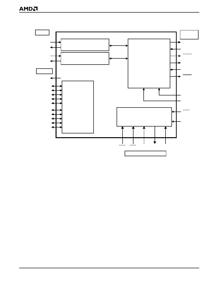
DSLAC Block Diagram . . . . . . . . . . . . . . . . . . . . . . . . . . . . . . . . . . . . . . . . . . . . 23
LIST OF TABLES
Table 1
A-Law: Positive Input Values . . . . . . . . . . . . . . . . . . . . . . . . . . . . . . . . . . . . . . . 44
Table 2
µ
-Law: Positive Input Values . . . . . . . . . . . . . . . . . . . . . . . . . . . . . . . . . . . . . . . 45
4
Am79C02/03/031(A) Data Sheet
BLOCK DIAGRAM
Dual SLAC Device
DCLK
Signal Processing
Channel 1 (CH 1)
Signal Processing
Channel 2 (CH 2)
PCM
Microprocessor Interface
(MPI)
Microprocessor
DXA
DRA
DXB
DRB
FS
PCLK
Time Slot Assigner
(TSA)
SLIC
Interface
(SLI)
09875H-001
SLIC
Analog
VIN
1
VOUT
1
VIN
2
VOUT
2
TSCA
TSCB
RST
C1
1
C2
1
C3
1
C4
1
C1
2
C2
2
C3
2
C4
2
C5
2
Highway
DOUT
DIN
MCLK
CHCLK
(02 only)
CS2
CS1
(02 & 031 only)
C5
1
(02 & 031 only)

SLAC Products
5
ORDERING INFORMATION
Standard Products
AMD standard products are available in several packages and operating ranges. The order number (Valid Combi-
nation) is formed by a combination of the elements below.
Am79C02/03/031
J
TEMPERATURE RANGE
C = Commercial (0
∞
C to 70
∞
C;
Relative Humidity=15% to 85%)*
PACKAGE TYPE
J =44-Pin Plastic Leaded Chip Carrier (PL 044)
--Am79C02
32-Pin Plastic Leaded Chip Carrier (PL 032)
--Am79C03 and 031
DEVICE NUMBER/DESCRIPTION
Am79C02/03/031
Dual Subscriber Line Audio-Processing Circuit (DSLAC Device)
Valid Combinations
Valid Combinations list configurations planned to
be supported in volume for this device. Consult
the local AMD sales office to confirm availability
of specific valid combinations, to check on newly
released combinations, and to obtain additional
data on AMD's standard military grade products.
C
Note:
* Functionality of the device from 0
∞
C to +70
∞
C is guaranteed by production testing. Performance from ≠40
∞
C to +85
∞
C is
guaranteed by characterization and periodic sampling of production units.
Valid Combinations
Am79C02
AJC, JC
Am79C03
Am79C031
A
DEVICE OPTIONS
Blank = Standard Device
A = Adaptive Transhybrid Balance