 | –≠–ª–µ–∫—Ç—Ä–æ–Ω–Ω—ã–π –∫–æ–º–ø–æ–Ω–µ–Ω—Ç: AM79R79 | –°–∫–∞—á–∞—Ç—å:  PDF PDF  ZIP ZIP |
Publication# 19752 Rev: G Amendment: /0
Issue Date: October 1999
Am79R79
Ringing Subscriber Line Interface Circuit
DISTINCTIVE CHARACTERISTICS
I Ideal for short-loop applications
I Ideal for ISDN terminal adaptor and fixed radio
access applications
I On-chip ringing with on-chip ring-trip detector
I Low standby state power
I Battery operation:
-- V
BAT1
: ≠40.5 V to ≠75 V
-- V
BAT2
: ≠19 V to V
BAT1
I On-chip battery switching and feed selection
I On-hook transmission
I Two-wire impedance set by single external
impedance
I Programmable constant-current feed
I Programmable Open Circuit voltage
I Programmable loop-detect threshold
I Current gain = 1000
I Ground-key detector
I Tip Open state for ground-start lines
I Polarity reversal option available
I Internal V
EE
regulator (no external ≠5 V power
supply required)
I Two on-chip relay drivers and snubber circuits
(32 PLCC)
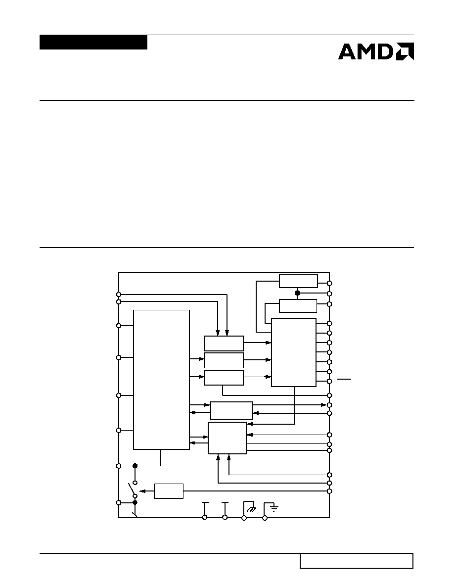
BLOCK DIAGRAM
E1
D2
D1
Two-Wire
Interface
HPA
HPB
Input Decoder
and Control
Relay
Driver
Ring-Trip
Detector
Power-Feed
Controller
RTRIP1
RTRIP2
BGND
VCC VNEG
RD
RDC
AGND/DGND
VBAT2
A(TIP)
B(RING)
RYOUT1
RDCR
C1
Switch
Driver
VBAT1
RSGL
Ground-Key
Detector
Off-Hook
Detector
Relay
Driver
RYOUT2
C2
C3
RSGH
B2EN
RSN
VTX
Signal
Transmission
RINGIN
RYE
DET

2
Am79R79 Data Sheet
GENERAL DESCRIPTION
The AMD family of subscriber line interface circuit
(SLIC) products provide the telephone interface func-
tions required throughout the worldwide market. AMD
SLIC devices address all major telephony markets in-
cluding central office (CO), private branch exchange
(PBX), digital loop carrier (DLC), fiber-in-the-loop
(FITL), radio-in-the-loop (RITL), hybrid fiber coax
(HFC), and video telephony applications.
The AMD SLIC devices offer support of BORSHT (bat-
tery feed, overvoltage protection, ringing, supervision,
hybrid, and test) functions with features including cur-
rent limiting, on-hook transmission, polarity reversal, Tip
Open, and loop-current detection. These features allow
reduction of linecard cost by minimizing component
count, conserving board space, and supporting auto-
mated manufacturing.
The AMD SLIC devices provide the two- to four-wire hy-
brid function, DC-loop feed, and two-wire supervision.
Two-wire termination is programmed by a scaled imped-
ance network. Transhybrid balance can be achieved with
an external balance circuit or simply programmed using
a companion AMD codec device, the Am79C02/03/031
DSLACTM device, the Am79Q02/021/03 Programmable
Quad SLAC (QSLACTM) device, or the Am79Q5457/4457
Nonprogrammable QSLAC device.
The Am79R79 Ringing SLIC device is a bipolar mono-
lithic SLIC that offers on-chip ringing. Now designers
can achieve significant cost reductions at the system
level for short-loop applications by integrating the ring-
ing function on chip. Examples of such applications
would be ISDN terminal adaptors, fiber-in-the-loop, ra-
dio-in-the-loop, hybrid fiber/coax and video telephony
(home-side) boxes. The Am79R79 Ringing SLIC can
provide sufficient voltage to meet the stringent LSSGR
five-ringer equivalent specification. Using a CMOS-
compatible input waveform and wave shaping R-C net-
work, the Am79R79 Ringing SLIC can provide trapezoi-
dal wave ringing to meet various design requirements.
In order to further enhance the suitability of this device
in short-loop, distributed switching applications, AMD
has maximized power savings by incorporating battery
switching on chip. The Am79R79 Ringing SLIC device
switches between two battery supplies such that in the
off-hook (active) state, a low battery is used to save
power. In order to meet the Open Circuit voltage require-
ments of fax machines and maintenance termination
units (MTU), the SLIC automatically switches to a higher
voltage in the on-hook (standby) state.
Like all of the AMD SLIC devices, the Am79R79 Ringing
SLIC device supports on-hook transmission, ring-trip
detection, programmable loop-detect threshold, and is
available with on-chip polarity reversal. The Am79R79
Ringing SLIC device is a programmable constant-cur-
rent feed device with two on-chip relay drivers to operate
external relays. Several performance grades are avail-
able to meet both CCITT and LSSGR requirements,
including various longitudinal balance options. This
unique device is available in the proven AMD 75 V bi-
polar process in the 32-pin PLCC package.

SLIC Products
3
ORDERING INFORMATION
Standard Products
Note:
* Functionality of the device from 0∞C to +70∞C is guaranteed by production testing. Performance from ≠40∞C to +85∞C is
guaranteed by characterization and periodic sampling of production units.
Am79R79
J
C
TEMPERATURE RANGE
C = Commercial (0∞C to 70∞C)*
PACKAGE TYPE
J = 32-pin Plastic Leaded Chip Carrier (PL 032)
DEVICE NUMBER/DESCRIPTION
Am79R79
JC
Valid Combinations
≠1
PERFORMANCE GRADE OPTION
≠1 = 52 dB Longitudinal Balance, Polarity Reversal
≠2 = 63 dB Longitudinal Balance, Polarity Reversal
≠3 = 52 dB Longitudinal Balance, No Polarity Reversal
≠4 = 63 dB Longitudinal Balance, No Polarity Reversal
Valid Combinations
≠1
≠2
≠3
≠4
Valid Combinations list configurations planned to
be supported in volume for this device. Consult
the local AMD sales office to confirm availability of
specific valid combinations, to check on newly
released combinations, and to obtain additional
data on AMD's standard military grade products.
AMD standard products are available in several packages and operating ranges. The order number (Valid Com-
bination) is formed by a combination of the elements below
Am79R79
Ringing Subscriber Line Interface Circuit
4
Am79R79 Data Sheet
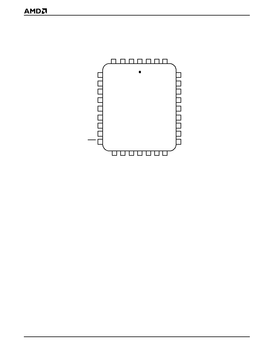
CONNECTION DIAGRAM
Top View
32-Pin PLCC
RTRIP1
4
3
2
1
32
31 30
25
24
23
22
21
20
19
18
17
16
15
14
13
12
11
10
9
8
7
6
5
D1
HPB
HPA
VNEG
RSN
26
27
28
29
RYOUT1
C2
RYE
VTX
B2EN
RDCR
RYOUT2
VBAT1
E1
C3
D2
NC
RDC
RTRIP2
RINGIN
VCC
VBAT
2
BGND
B(RING)
A(T
I
P)
RD
C1
RSGH
RSGL
AGND/DGND
Notes:
1. Pin 1 is marked for orientation.
2. NC = No connect
DET

SLIC Products
5
PIN DESCRIPTIONS
Pin Names
Type
Description
AGND/DGND
Gnd
Analog and Digital ground
A(TIP)
Output
Output of A(TIP) power amplifier
B2EN
Input
VBAT2 Enable. Logic Low enables operation from V
BAT2
. Logic High enables operation
from V
BAT1
. TTL compatible.
BGND
Gnd
Battery (power) ground
B(RING)
Output
Output of B(RING) power amplifier
C3≠C1
Input
Decoder. TTL compatible. C3 is MSB and C1 is LSB.
D1
Input
Relay1 Control. TTL compatible. Logic Low activates the Relay1 relay driver.
D2
Input
(Option) Relay2 Control. TTL compatible. Logic Low activates the Relay2 relay driver.
DET
Output
Switchhook Detector. Logic Low indicates that the selected detector is tripped. Logic inputs
C3≠C1 and E1 select the detector. Open-collector with a built-in 15 k
pull-up resistor.
E1
Input
(Option) Ground-Key Enable. A logic High selects the off-hook detector. A logic Low selects
the ground-key detector. TTL compatible.
HPA
Capacitor
High-pass filter capacitor. A(TIP) side of high-pass filter capacitor.
HPB
Capacitor
High-pass filter capacitor. B(RING) side of high-pass filter capacitor.
RD
Resistor
Detector resistor. Detector threshold set and filter pin.
RDC
Resistor
DC feed resistor. Connection point for the DC feed current programming network, which
also connects to the receiver summing node (RSN). V
RDC
is negative for normal polarity
and positive for reverse polarity.
RDCR
--
Connection point for feedback during ringing.
RINGIN
Input
Ring Signal Input. Pin for ring signal input. Square-wave shaped by external RC filter.
Requires 50% duty cycle. CMOS-compatible input.
RSGH
Input
Saturation Guard High. Pin for resistor to adjust Open Circuit voltage when operating from
V
BAT1
.
RSGL
Input
Saturation Guard Low. Pin for resistor to adjust the anti-saturation cut-in voltage when
operating from both V
BAT1 and
V
BAT2
.
RSN
Input
Receive Summing Node. The metallic current (AC and DC) between A(TIP) and B(RING)
is equal to 1000 x the current into this pin. The networks that program receive gain, two-wire
impedance, and feed resistance all connect to this node.
RTRIP1
Input
Ring-trip detector. Ring-trip detector threshold set and filter pin.
RTRIP2
Input
Ring-trip detector. Ring-trip detector threshold offset (switch to V
BAT1
). For power
conservation in any nonringing state, this switch is open.
RYE
Output
Common Emitter of RYOUT1/RYOUT2. Emitter output of RYOUT1 and RYOUT2. Normally
connected to relay ground.
RYOUT1
Output
Relay/switch driver. Open-collector driver with emitter internally connected to RYE.
RYOUT2
Output
(Option) Relay/switch driver. Open-collector driver emitter internally connected to RYE.
VBAT1
Battery
Battery supply and connection to substrate.
VBAT2
Battery
Power supply to output amplifiers. Connect to off-hook battery through a diode.
VCC
Power
Positive analog power supply.
VNEG
Power
Negative analog power supply. This pin is the return for the intern VEE regulator.
VTX
Output
Transmit Audio. This output is 0.5066 gain version of the A(TIP) and B(RING) metallic
voltage. VTX also sources the two-wire input impedance programming network.