Publication# 11419
Rev. D
Amendment /0
Issue Date: May 1995
2-10
Advanced
Micro
Devices
Am27C64
64 Kilobit (8,192 x 8-Bit) CMOS EPROM
FINAL
DISTINCTIVE CHARACTERISTICS
s
Fast access time
-- 45 ns
s
Low power consumption
-- 20
µ
A typical CMOS standby current
s
JEDEC-approved pinout
s
Single +5 V power supply
s
±
10% power supply tolerance available
s
100% Flashrite
TM
programming
-- Typical programming time of 1 second
s
Latch-up protected to 100 mA from ≠1 V to
V
CC
+ 1 V
s
High noise immunity
s
Versatile features for simple interfacing
-- Both CMOS and TTL input/output
compatibility
-- Two line control functions
s
Standard 28-pin DIP, PDIP, and 32-pin PLCC
packages
GENERAL DESCRIPTION
The Am27C64 is a 64-Kbit ultraviolet erasable program-
mable read-only memory. It is organized as 8K words by
8 bits per word, operates from a single +5 V supply, has
a static standby mode, and features fast single address
location programming. Products are available in win-
dowed ceramic DIP packages as well as plastic one
time programmable (OTP) PDIP, and PLCC packages.
Typically, any byte can be accessed in less than 45 ns,
allowing operation with high-performance microproces-
sors without any WAIT states. The Am27C64 offers
separate Output Enable (
OE
) and Chip Enable (
CE
)
controls, thus eliminating bus contention in a multiple
bus microprocessor system.
AMD's CMOS process technology provides high speed,
low power, and high noise immunity. Typical power con-
sumption is only 80 mW in active mode, and 100
µ
W in
standby mode.
All signals are TTL levels, including programming sig-
nals. Bit locations may be programmed singly, in blocks,
or at random. The Am27C64 supports AMD's Flashrite
programming algorithm (100
µ
s pulses) resulting in a
typical programming time of 1 second.
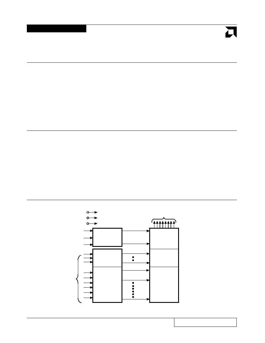
BLOCK DIAGRAM
V
CC
V
SS
Output Enable
Chip Enable
and
Prog Logic
Y
Decoder
X
Decoder
CE
OE
Output
Buffers
Y
Gating
65,538
Bit Cell
Matrix
A0≠A12
Address
Inputs
Data Outputs
DQ0≠DQ7
11419D-1
V
PP
PGM
AMD
2-11
Am27C64
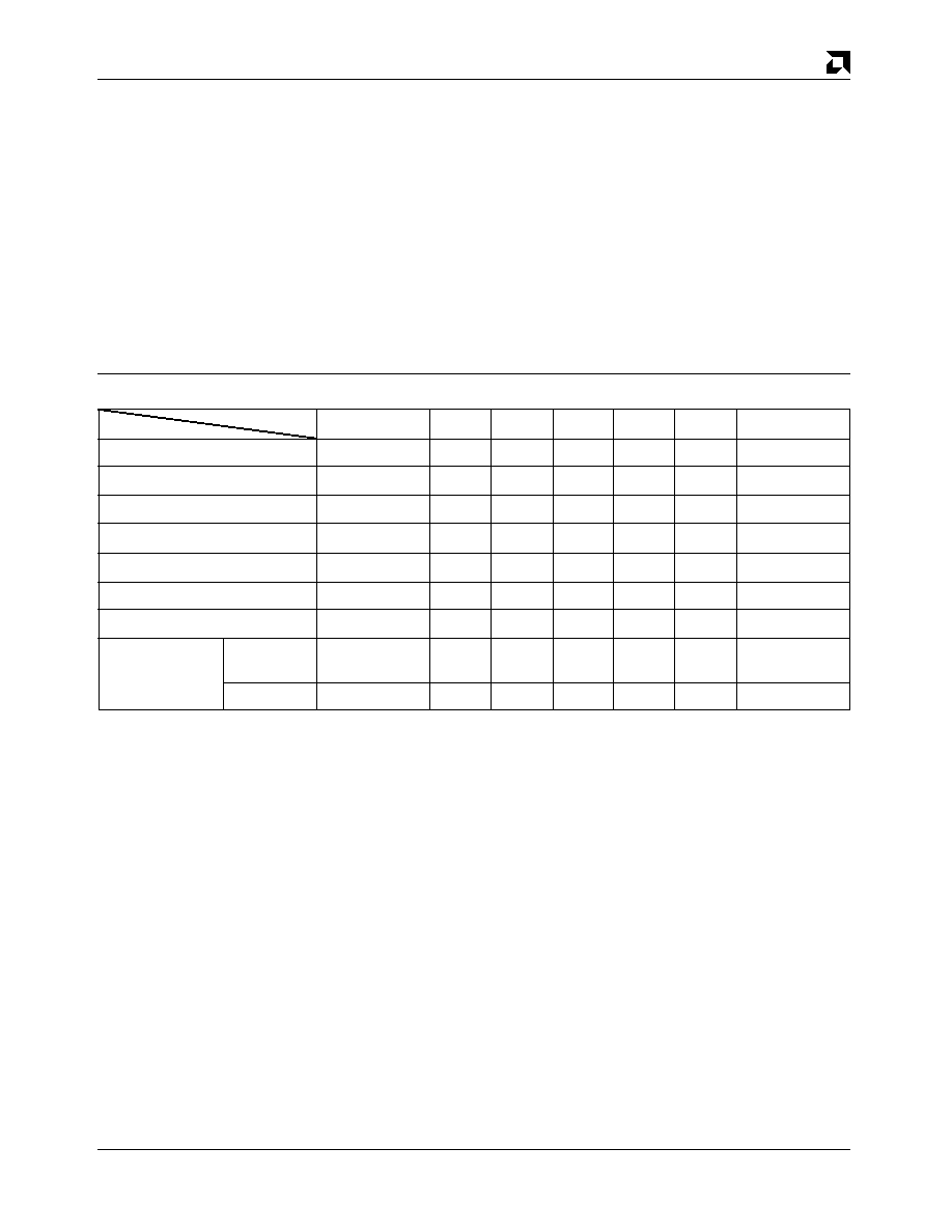
PRODUCT SELECTOR GUIDE
Family Part No.
Am27C64
Ordering Part No:
V
CC
±
5%
-255
V
CC
±
10%
-45
-55
-70
-90
-120
-150
-200
Max Access Time (ns)
45
55
70
90
120
150
200
250
CE
(
E
) Access Time (ns)
45
55
70
90
120
150
200
250
OE
(
G
) Access Time (ns)
30
35
40
40
50
50
50
50
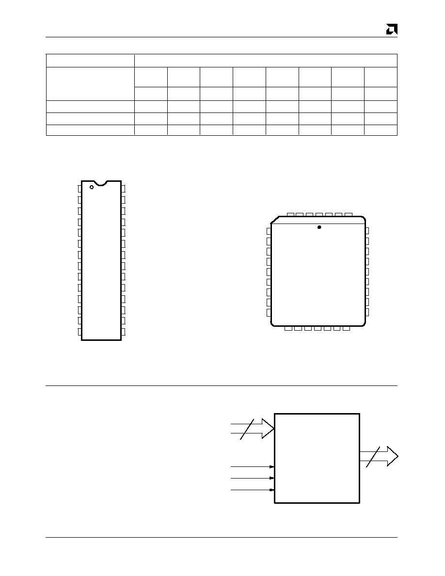
CONNECTION DIAGRAMS
Top View
DIP
Notes:
1. JEDEC nomenclature is in parentheses.
PLCC
V
PP
V
CC
A9
A11
A12
PGM
(
P
)
A8
DQ7
1
3
5
7
9
11
12
10
2
4
8
6
13
14
28
26
24
22
20
18
17
19
27
25
21
23
16
15
A7
A6
A5
A4
A3
A2
A1
A0
V
SS
DQ2
DQ1
DQ0
OE
(
G
)
A10
CE
(
E
)
DQ6
DQ5
DQ4
DQ3
NC
11419D-2
11419D-3
1
31 30
2
3
4
5
6
7
8
9
10
11
12
13
17 18 19 20
16
15
14
29
28
27
26
25
24
23
22
21
32
A6
A5
A4
A3
A2
A1
A0
NC
DQ0
A8
A9
A11
NC
OE
(
G
)
A10
CE
(
E
)
DQ7
A7
A12
V
PP
DU
V
CC
PGM (
P
)
NC
DQ1
DQ2
V
SS
DU
DQ3
DQ4
DQ5
DQ6
LOGIC SYMBOL
PIN DESIGNATIONS
A0≠A12
=
Address Inputs
CE
(
E
)
=
Chip Enable
DQ0≠DQ7
=
Data Inputs/Outputs
OE
(
G
)
=
Output Enable Input
PGM
(
P
)
=
Program Enable Input
V
CC
=
V
CC
Supply Voltage
V
PP
=
Program Voltage Input
V
SS
=
Ground
NC
=
No Internal Connection
DU
=
No External Connection (Don't Use)
11419D-4
CE
(
E
)
OE
(
G
)
DQ0≠DQ7
A0≠A12
13
8
PGM
(
P
)
AMD
2-12
Am27C64
ORDERING INFORMATION
UV EPROM Products
Valid Combinations list configurations planned to be
supported in volume for this device. Consult the lo-
cal AMD sales office to confirm availability of specific
valid combinations and to check on newly released
combinations.
DEVICE NUMBER
Am27C64
64 Kilobit (8,192 x 8-Bit) CMOS UV EPROM
PACKAGE TYPE
D = 28-Pin Ceramic DIP (CDV028)
Valid Combinations
AMD Standard products are available in several packages and operating ranges. The order number (Valid Combination) is
formed by a combination of:
Valid Combinations
B
C
D
-45
AM27C64
OPTIONAL PROCESSING
Blank = Standard Processing
B = Burn-in
TEMPERATURE RANGE
C = Commercial (0
∞
C to +70
∞
C)
I
= Industrial (≠40
∞
C to +85
∞
C)
E = Extended Commercial (≠55
∞
C to +125
∞
C)
SPEED OPTION
See Product Selector Guide and Valid Combinations
AM27C64-55
AM27C64-70
DC, DCB, DI, DIB
AM27C64-90
AM27C64-120
AM27C64-150
AM27C64-200
AM27C64-255
DC, DCB, DI,
DIB, DE, DEB
AM27C64-45
DC, DCB, DI, DIB
AMD
2-13
Am27C64
ORDERING INFORMATION
OTP Products
DEVICE NUMBER
Am27C64
64 Kilobit (8,192 x 8-Bit) CMOS OTP EPROM
Valid Combinations
AM27C64-90
AM27C64-120
AM27C64-150
AM27C64-200
AM27C64-255
PACKAGE TYPE
P = 28-Pin Plastic DIP (PD 028)
J = 32-Pin Rectangular Plastic Leaded Chip
Carrier (PL 032)
AMD Standard products are available in several packages and operating ranges. The order number (Valid Combination) is
formed by a combination of:
C
P
-55
AM27C64
OPTIONAL PROCESSING
Blank = Standard Processing
TEMPERATURE RANGE
C = Commercial (0
∞
C to +70
∞
C)
I
= Industrial (≠40
∞
C to + 85
∞
C)
E = Extended Commercial (≠55
∞
C to +125
∞
C)
SPEED OPTION
See Product Selector Guide and Valid Combinations
JC, PC,
JI, PI
AM27C64-70
AM27C64-55
Valid Combinations
Valid Combinations list configurations planned to be
supported in volume for this device. Consult the lo-
cal AMD sales office to confirm availability of specific
valid combinations and to check on newly released
combination.

AMD
2-14
Am27C64
FUNCTIONAL DESCRIPTION
Erasing the Am27C64
In order to clear all locations of their programmed con-
tents, it is necessary to expose the Am27C64 to an
ultraviolet light source. A dosage of 15 W seconds/cm
2
is
required to completely erase an Am27C64. This dosage
can be obtained by exposure to an ultraviolet lamp--
wavelength of 2537 A
∞
--with intensity of 12,000
µ
W/cm
2
for 15 to 20 minutes. The Am27C64 should be directly
under and about one inch from the source and all filters
should be removed from the UV light source prior
to erasure.
It is important to note that the Am27C64 and similar
devices will erase with light sources having wavelengths
shorter than 4000 A
∞
. Although erasure times will be
much longer than with UV sources at 2537 A
∞
, exposure
to fluorescent light and sunlight will eventually erase the
Am27C64 and exposure to them should be prevented to
realize maximum system reliability. If used in such an
environment, the package window should be covered
by an opaque label or substance.
Programming the Am27C64
Upon delivery or after each erasure the Am27C64
has all 65,536 bits in the "ONE" or HIGH state. "ZEROs"
are loaded into the Am27C64 through the procedure
of programming.
The programming mode is entered when 12.75 V
±
0.25 V is applied to the V
PP
pin,
CE
is at V
IL
and
PGM
is
at V
IL
.
For programming, the data to be programmed is applied
8 bits in parallel to the data output pins.
The Flashrite algorithm reduces programming time by
using 100
µ
s programming pulses and by giving each
address only as many pulses as is necessary in order to
reliably program the data. After each pulse is applied to
a given address, the data in that address is verified. If
the data does not verify, additional pulses are given until
it verifies or the maximum is reached. This process is
repeated while sequencing through each address of the
Am27C64. This part of the algorithm is done at
V
CC
= 6.25 V to assure that each EPROM bit is pro-
grammed to a sufficiently high threshold voltage. After
the final address is completed, the entire EPROM mem-
ory is verified at V
CC
= V
PP
= 5.25 V.
Please refer to Section 6 for programming flow chart
and characteristics.
Program Inhibit
Programming of multiple Am27C64 in parallel with dif-
ferent data is also easily accomplished. Except for
CE
,
all like inputs of the parallel Am27C64 may be common.
A TTL low-level program pulse applied to an Am27C64
PGM
input with V
PP
= 12.75 V
±
0.25 V and
CE
Low will
program that Am27C64. A high-level
CE
input inhibits
the other Am27C64 devices from being programmed.
Program Verify
A verify should be performed on the programmed bits to
determine that they were correctly programmed. The
verify should be performed with
OE
and
CE
at V
IL
,
PGM
at V
IH,
and V
PP
between 12.5 V and 13.0 V.
Auto Select Mode
The auto select mode allows the reading out of a binary
code from an EPROM that will identify its manufacturer
and type. This mode is intended for use by programming
equipment for the purpose of automatically matching
the device to be programmed with its corresponding
programming algorithm. This mode is functional in the
25
∞
C
±
5
∞
C ambient temperature range that is required
when programming the Am27C64.
To activate this mode, the programming equipment
must force 12.0 V
±
0.5 V on address line A9 of the
Am27C64. Two identifier bytes may then be sequenced
from the device outputs by toggling address line A0 from
V
IL
to V
IH
. All other address lines must be held at V
IL
dur-
ing auto select mode.
Byte 0 (A
0
= V
IL
) represents the manufacturer code, and
byte 1 (A
0
= V
IH
), the device code. For the Am27C64,
these two identifier bytes are given in the Mode Select
Table. All identifiers for manufacturer and device codes
will possess odd parity, with the MSB (DQ7) defined as
the parity bit.
Read Mode
The Am27C64 has two control functions, both of which
must be logically satisfied in order to obtain data at the
outputs. Chip Enable (
CE
) is the power control and
should be used for device selection. Output Enable (
OE
)
is the output control and should be used to gate data to
the output pins, independent of device selection. As-
suming that addresses are stable, address access time
(t
ACC
) is equal to the delay from
CE
to output (t
CE
). Data
is available at the outputs t
OE
after the falling edge of
OE
, assuming that
CE
has been LOW and addresses
have been stable for at least t
ACC
≠t
OE
.
Standby Mode
The Am27C64 has a CMOS standby mode which re-
duces the maximum V
CC
current to 100
µ
A. It is placed in
CMOS-standby when
CE
is at V
CC
±
0.3 V. The
Am27C64 also has a TTL-standby mode which reduces
the maximum V
CC
current to 1.0 mA. It is placed in
TTL-standby when
CE
is at V
IH
. When in standby mode,
the outputs are in a high-impedance state, independent
of the
OE
input.
AMD
2-15
Am27C64
Output OR-Tieing
To accommodate multiple memory connections, a two-
line control function is provided to allow for:
s
Low memory power dissipation
s
Assurance that output bus contention will not occur
It is recommended that
CE
be decoded and used as the
primary device-selecting function, while
OE
be made a
common connection to all devices in the array and con-
nected to the READ line from the system control bus.
This assures that all deselected memory devices are in
low-power standby mode and that the output pins are
only active when data is desired from a particular
memory device.
System Applications
During the switch between active and standby condi-
tions, transient current peaks are produced on the rising
and falling edges of Chip Enable. The magnitude of
these transient current peaks is dependent on the out-
put capacitance loading of the device. At a minimum, a
0.1-
µ
F ceramic capacitor (high frequency, low inherent
inductance) should be used on each device between
V
CC
and V
SS
to minimize transient effects. In addition, to
overcome the voltage drop caused by the inductive ef-
fects of the printed circuit board traces on EPROM ar-
rays, a 4.7-
µ
F bulk electrolytic capacitor should be used
between V
CC
and V
SS
for each eight devices. The loca-
tion of the capacitor should be close to where the power
supply is connected to the array.
MODE SELECT TABLE
CE
OE
PGM
A0
A9
V
PP
Outputs
Read
V
IL
V
IL
X
X
X
X
D
OUT
Output Disable
X
V
IH
X
X
X
X
High-Z
Standby (TTL)
V
IH
X
X
X
X
X
High-Z
Standby (CMOS)
V
CC
±
0.3 V
X
X
X
X
X
High-Z
Program
V
IL
X
V
IL
X
X
V
PP
D
IN
Program Verify
V
IL
V
IL
V
IH
X
X
V
PP
D
OUT
Program Inhibit
V
IH
X
X
X
X
V
PP
High-Z
Manufacturer
Code
V
IL
V
IL
X
V
IL
V
H
X
01H
Device Code
V
IL
V
IL
X
V
IH
V
H
X
15H
Auto Select
(Note 3)
Mode
Pins
Notes:
1. V
H
= 12.0 V
±
0.5 V
2. X = Either V
IH
or V
IL
3. A1≠A8 = A10≠A12
= V
IL
4. See DC Programming Characteristics for V
PP
voltage during programming.

AMD
2-16
Am27C64
ABSOLUTE MAXIMUM RATINGS
Storage Temperature
OTP Products
≠65
∞
C to +125
∞
C
. . . . . . . . . . . . . . .
All Other Products
≠65
∞
C to +150
∞
C
. . . . . . . . . . . .
Ambient Temperature
with Power Applied
≠55
∞
C to +125
∞
C
. . . . . . . . . . . . .
Voltage with Respect To V
SS
All pins except A9,V
PP
,V
CC
≠0.6 V to V
CC
+ 0.5 V
.
A9
and V
PP
≠0.6 V to +13.5 V
. . . . . . . . . . . . . . . .
V
CC
≠0.6 V to +7.0 V
. . . . . . . . . . . . . . . . . . . . . . .
Notes:
1. Minimum DC voltage on input or I/O pins is ≠0.5 V. During
transitions, the inputs may overshoot V
SS
to ≠2.0 V for pe-
riods of up to 20 ns. Maximum DC voltage on input and I/O
pins is V
CC
+ 0.5 V which may overshoot to V
CC
+ 2.0 V for
periods up to 20 ns.
2. For A9 and V
PP
the minimum DC input is ≠0.5 V. During
transitions, A9 and V
PP
may overshoot V
SS
to ≠2.0 V for
periods of up to 20 ns. A9 and V
PP
must not exceed 13.5 V
for any period of time.
Stresses above those listed under "Absolute Maximum Rat-
ings" may cause permanent damage to the device. This is a
stress rating only; functional operation of the device at these
or any other conditions above those indicated in the opera-
tional sections of this specification is not implied. Exposure of
the device to absolute maximum rating conditions for ex-
tended periods may affect device reliability.
OPERATING RANGES
Commercial (C) Devices
Ambient Temperature (T
A
)
0
∞
C to +70
∞
C
. . . . . . .
Industrial (I) Devices
Ambient Temperature (T
A
)
≠40
∞
C to +85
∞
C
. . . . .
Extended Commercial (E) Devices
Ambient Temperature (T
A
)
≠55
∞
C to +125
∞
C
. . . .
Supply Read Voltages
V
CC
for Am27C64-XX5
+4.75 V to +5.25 V
. . . . . .
V
CC
for Am27C64-XX0
+4.50 V to +5.50 V
. . . . . .
Operating ranges define those limits between which the func-
tionality of the device is guaranteed.
AMD
2-17
Am27C64
DC CHARACTERISTICS over operating range unless otherwise specified.
(Notes 1, 2, 3 and 4)
Parameter
Symbol
Parameter Description
Test Conditions
Min
Max
Unit
V
OH
Output HIGH Voltage
I
OH
= ≠400
µ
A
2.4
V
V
OL
Output LOW Voltage
I
OL
= 2.1 mA
0.45
V
V
IH
Input HIGH Voltage
2.0
V
CC
+ 0.5
V
V
IL
Input LOW Voltage
≠0.5
+0.8
V
I
LI
Input Load Current
V
IN
= 0 V to V
CC
1.0
µ
A
I
LO
Output Leakage Current
V
OUT
= 0 V to V
CC
C/I Devices
1.0
E Devices
5.0
I
CC1
V
CC
Active Current
CE
= V
IL
, f = 10 MHz,
25
mA
(Note 3)
I
OUT
= 0 mA
I
CC2
V
CC
TTL Standby Current
CE
= V
IH
1
mA
I
CC3
V
CC
CMOS Standby Current
CE
= V
CC
±
0.3 V
100
µ
A
I
PP1
V
PP
Current During Read
CE
=
OE
= V
IL
, V
PP
= V
CC
100
µ
A
µ
A
Notes:
1. V
CC
must be applied simultaneously or before V
PP
, and removed simultaneously or after V
PP
.
2. Caution: The Am27C64 must not be removed from (or inserted into) a socket when V
CC
or V
PP
is applied.
3. I
CC1
is tested with
OE
= V
IH
to simulate open outputs.
4. Minimum DC Input Voltage is ≠0.5 V. During transitions, the inputs may overshoot to ≠2.0 V for periods less than 20 ns.
Maximum DC Voltage on output pins is V
CC
+ 0.5 V, which may overshoot to V
CC
+ 2.0 V for periods less than 20 ns.
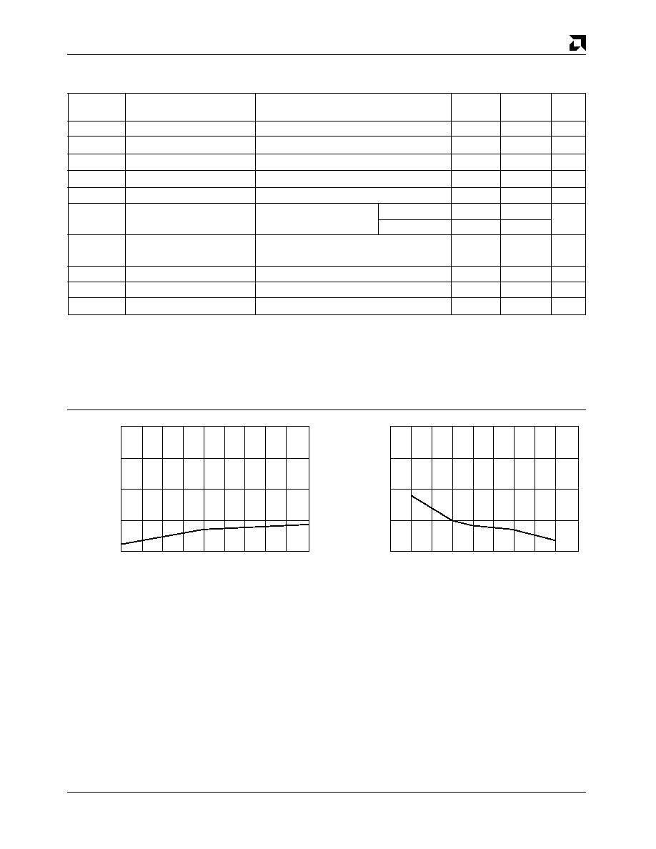
≠75 ≠50 ≠25 0
25
50
75 100 125 150
30
25
20
15
10
Frequency in MHz
11419D-6
1
2
3
4
5
6
7
8
9
10
30
25
20
15
10
Supply Current
in mA
Supply Current
in mA
Temperature in
∞
C
Figure 1. Typical Supply Current
vs. Frequency
V
CC
= 5.5 V, T = 25
∞
C
Figure 2. Typical Supply Current
vs. Temperature
V
CC
= 5.5 V, f = 10 MHz
11419D-5
AMD
2-18
Am27C64
CAPACITANCE
Parameter
Test
Symbol
Parameter Description
Conditions
Typ
Max
Typ
Max
Typ
Max
Unit
C
IN
Input Capacitance
V
IN
= 0
8
10
6
10
5
10
pF
C
OUT
Output Capacitance
V
OUT
= 0
11
14
8
12
8
10
pF
Notes:
1. This parameter is only sampled and not 100% tested.
2. T
A
= +25
∞
C, f = 1 MHz.
CDV028
PL 032
PD 028
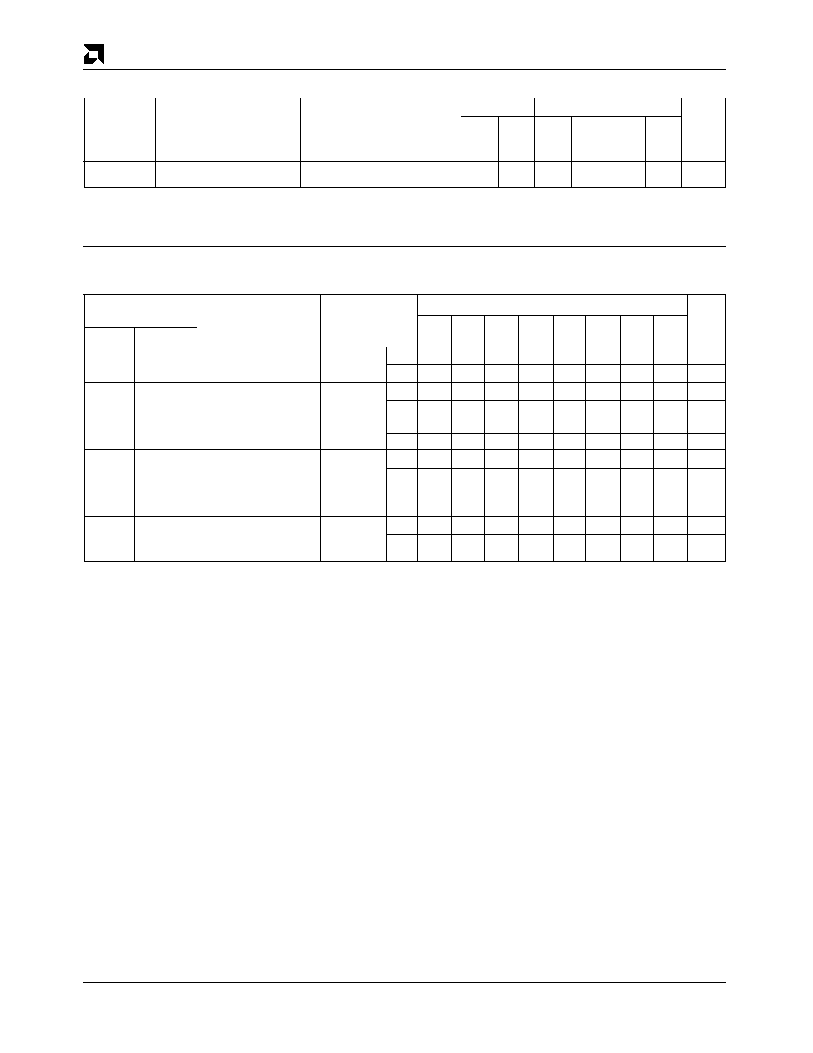
SWITCHING CHARACTERISTICS over operating range unless otherwise specified
(Notes 1, 3 and 4)
Parameter
Test
JEDEC
Standard Description
Conditions
-45
-55
-70
-90
-120
-150
-200
-255
Unit
t
AVQV
t
ACC
Address to
CE
=
OE
=
Min
≠
≠
≠
≠
≠
≠
≠
≠
Output Delay
V
IL
Max
45
55
70
90
120
150
200
250
ns
t
ELQV
t
CE
Chip Enable to
OE
= V
IL
Min
≠
≠
≠
≠
≠
≠
≠
≠
Output Delay
Max
45
55
70
90
120
150
200
250
ns
t
GLQV
t
OE
Output Enable to
CE
= V
IL
Min
≠
≠
≠
≠
≠
≠
≠
≠
Output Delay
Max
30
35
40
40
50
50
50
50
ns
t
EHQZ
t
DF
Min
≠
≠
≠
≠
≠
≠
≠
≠
t
GHQZ
(Note 2)
Max
25
25
25
25
30
30
30
30
ns
t
AXQX
t
OH
Output Hold from
Min
0
0
0
0
0
0
0
0
Addresses,
CE
, or
OE
,
Max
≠
≠
≠
≠
≠
≠
≠
≠
ns
whichever occurred first
Parameter
Symbols
Am27C64
Notes:
1. V
CC
must be applied simultaneously or before V
PP
, and removed simultaneously or after V
PP
.
2. This parameter is only sampled and not 100% tested.
3. Caution: The Am27C64 must not be removed from (or inserted into) a socket or board when V
PP
or V
CC
is applied.
4. For the -45, -55 and -70:
Output Load: 1 TTL gate and C
L
= 30 pF
Input Rise and Fall Times: 20 ns
Input Pulse Levels: 0 V to 3 V
Timing Measurement Reference Level: 1.5 V for inputs and outputs
For all other versions:
Output Load: 1 TTL gate and C
L
= 100 pF
Input Rise and Fall Times: 20 ns
Input Pulse Levels: 0.45 V to 2.4 V
Timing Measurement Reference Level: 0.8 V and 2 V inputs and outputs
Chip Enable HIGH or
Output Enable HIGH,
whichever comes
first, to Output Float

AMD
2-19
Am27C64
SWITCHING TEST CIRCUIT
Device
Under
Test
C
L
+5.0 V
C
L
= 100 pF including jig capacitance (30 pF for -45, -55, -70)
6.2 k
2.7 k
Diodes = IN3064
or Equivalent
11419D-7
SWITCHING TEST WAVEFORM
2.4 V
0.45 V
2.0 V
0.8 V
2.0 V
0.8 V
Test Points
Input
Output
3 V
0 V
1.5 V
1.5 V
Input
Output
Test Points
AC Testing: Inputs are driven at 2.4 V for a logic "1"
and 0.45 V for a logic "0". Input pulse
rise and fall times are
20 ns.
11419D-8
AC Testing: Inputs are driven at 3.0 V for a logic "1"
and 0 V for a logic "0". Input pulse rise and
fall times are
20 ns for -45, -55 and -70.

AMD
2-20
Am27C64
KEY TO SWITCHING WAVEFORMS
Must Be
Steady
May
Change
from H to L
May
Change
from L to H
Does Not
Apply
Don't Care,
Any Change
Permitted
Will Be
Steady
Will Be
Changing
from H to L
Will Be
Changing
from L to H
Changing
State
Unknown
Center
Line is High
Impedence
"Off" State
WAVEFORM
INPUTS
OUTPUTS
KS000010
SWITCHING WAVEFORMS
11419D-9
Addresses
CE
OE
Output
Addresses Valid
High Z
High Z
t
CE
Valid Output
2.4
0.45
2.0
0.8
2.0
0.8
t
ACC
(Note 1)
t
OE
t
DF
(Note 2)
t
OH
Notes:
1.
OE
may be delayed up to t
ACC
≠t
OE
after the falling edge of the addresses without impact on t
ACC
.
2. t
DF
is specified from
OE
or
CE
, whichever occurs first.