This document contains information on a product under development at Advanced Micro Devices. The information is
intended to help you evaluate this product. AMD reserves the right to change or discontinue work on this proposed
product without notice.
Advanced
Micro
Devices
DISTINCTIVE CHARACTERISTICS
s
High-Performance Design
-- Industry-standard write-back cache support
-- Frequent instructions execute in one clock
-- 105.6-million bytes/second burst bus at 33 MHz
-- Flexible write-through and write-back address
control
-- Advanced 0.35-
µ
CMOS-process technology
-- Dynamic bus sizing for 8-, 16-, and 32-bit buses
-- Supports "soft reset" capability
s
High On-Chip Integration
-- 16-Kbyte unified code and data cache
-- Floating-point unit
-- Paged, virtual memory management
s
Enhanced System and Power Management
-- Stop clock control for reduced power
consumption
-- Industry-standard two-pin System Management
Interrupt (SMI) for power management indepen-
dent of processor operating mode and operating
system
-- Static design with Auto Halt power-down support
-- Wide range of chipsets supporting SMM avail-
able to allow product differentiation
s
Complete 32-Bit Architecture
-- Address and data buses
-- All registers
-- 8-, 16-, and 32-bit data types
s
Standard Features
-- 3-V core with 5-V tolerant I/O
-- Available in a 133-MHz version
-- Binary compatible with all Am486
Æ
DX,
Am486DX2, and Am486DX4 microprocessors
-- Wide range of chipsets and support available
through the AMD FusionPC
SM
Program
s
168-pin PGA package or 208-pin SQFP package
s
IEEE 1149.1 JTAG Boundary-Scan Compatibility
s
Supports Environmental Protection Agency's
Energy Star program
-- 3-V operation reduces power consumption up to
40%
-- Energy management capability provides excel-
lent base for energy-efficient design
-- Works with a variety of energy-efficient, power-
managed devices
GENERAL DESCRIPTION
The Am5
X
86TM microprocessor is an addition to the AMD
microprocessor product family. The new processor en-
hances system performance by raising the microproces-
sor operating frequency to the highest levels allowed by
current manufacturing technology, while maintaining
complete compatibility with the standard Am486 proces-
sor architecture and Microsoft
Æ
Windows
Æ
. The CPUs
incorporate write-back cache, flexible clock control, and
enhanced SMM. Table 1 shows available processors
in the Am5
X
86 microprocessor family.
The Am5
X
86 microprocessor family allows write-back
configuration through software and cacheable access
control. On-chip cache lines are configurable as either
write-through or write-back. The CPU clock control fea-
ture permits the CPU clock to be stopped under con-
trolled conditions, allowing reduced power consumption
during system inactivity. The SMM function is implement-
ed with an industry standard two-pin interface.
Table 1. Clocking Options
Operating
Frequency
Input Clock
Available Package
133 MHz
33 MHz
168-pin PGA
133 MHz
33 MHz
208-pin SQFP
PRELIMINARY
Am5
X
86TM
Microprocessor Family
Publication # 19751 Rev: C Amendment/0
Issue Date: March 1996
2
Am5
X
86 Microprocessor
AMD
PRELIMINARY
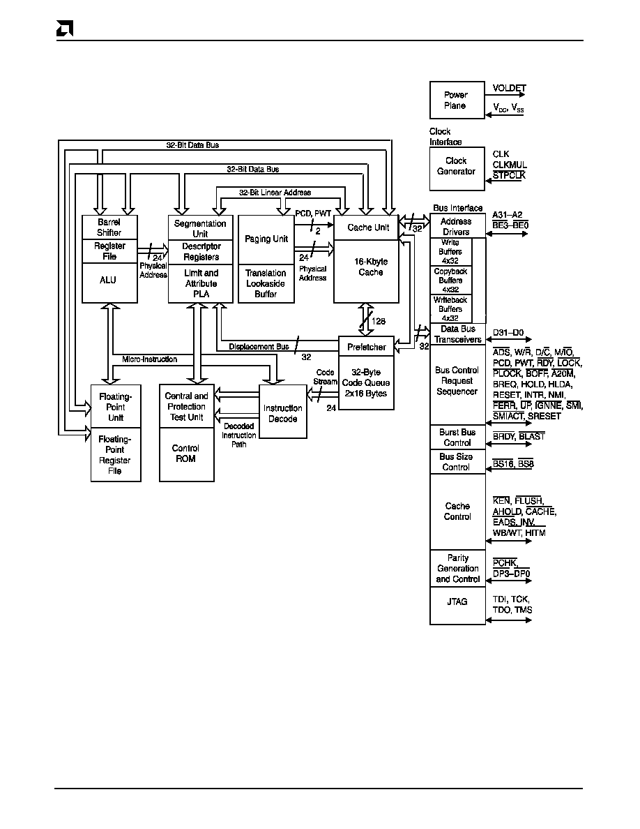
BLOCK DIAGRAM
AMD
PRELIMINARY
Am5
X
86 Microprocessor
3
ORDERING INFORMATION
Standard Products
AMD standard products are available in several packages and operating ranges. The order number (Valid Combination) is
formed by a combination of the elements below.
A
AMD-X5
Package Type
Family/Core
Valid Combinations
Valid Combinations list configura-
tions planned to be supported in vol-
ume for this device. Consult the local
AMD sales office to confirm avail-
ability of specific valid combinations
and to check on newly released
combinations.
A =168-pin PGA
S = 208-pin SQFP
AMD-X5
Case Temperature
D
W= 55∞ C
Z = 85∞ C
≠ 133
Clock Speed
133 = 133 MHz
W
Operating Voltage
D = 3.45 V
F = 3.3 V
Valid Combinations
OPN
Package Type
Operating Voltage
Case Temperature
(Max)
AMD-X5-133ADW
PGA
3.45 V
55∞ C
AMD-X5-133ADZ
PGA
3.45 V
85∞ C
AMD-X5-133SFZ
SQFP
3.3 V
85∞ C
AMD-X5-133SDZ
SQFP
3.45 V
85∞ C

4
Am5
X
86 Microprocessor
AMD
PRELIMINARY
Table of Contents
1
Connection Diagrams and Pin Designations ......................................................................................... 8
1.1 168-Pin PGA (Pin Grid Array) Package .......................................................................................... 8
1.2 168-Pin PGA Designations (Functional Grouping) ......................................................................... 9
1.3 208-Pin SQFP (Shrink Quad Flat Pack) Package ........................................................................ 10
1.4 208-Pin SQFP Designations (Functional Grouping) ..................................................................... 11
2
Logic Symbol ...................................................................................................................................... 12
3
Pin Description .................................................................................................................................... 13
4
Functional Description ........................................................................................................................ 18
4.1 Overview ....................................................................................................................................... 18
4.2 Memory ......................................................................................................................................... 18
4.3 Modes of Operation ...................................................................................................................... 18
4.3.1 Real mode ........................................................................................................................... 18
4.3.2 Virtual mode ........................................................................................................................ 18
4.3.3 Protected mode ................................................................................................................... 18
4.3.4 System Management mode ................................................................................................ 18
4.4 Cache Architecture ....................................................................................................................... 18
4.4.1 Write-Through Cache .......................................................................................................... 18
4.4.2 Write-Back Cache ............................................................................................................... 18
4.5 Write-Back Cache Protocol ........................................................................................................... 19
4.5.1 Cache Line Overview .......................................................................................................... 19
4.5.2 Line Status and Line State .................................................................................................. 19
4.5.2.1 Invalid ......................................................................................................................... 19
4.5.2.2 Exclusive .................................................................................................................... 19
4.5.2.3 Shared ....................................................................................................................... 19
4.5.2.4 Modified ..................................................................................................................... 19
4.6 Cache Replacement Description .................................................................................................. 20
4.7 Memory Configuration ................................................................................................................... 20
4.7.1 Cacheability ......................................................................................................................... 20
4.7.2 Write-Through/Write-Back ................................................................................................... 20
4.8 Cache Functionality in Write-Back mode ...................................................................................... 20
4.8.1 Processor-Initiated Cache Functions and State Transitions ............................................... 20
4.8.2 Snooping Actions and State Transitions ............................................................................. 21
4.8.2.1 Difference between Snooping Access Cases ............................................................ 21
4.8.2.2 HOLD Bus Arbitration Implementation ....................................................................... 22
4.8.2.2.1 Processor-Induced Bus Cycles ........................................................................ 22
4.8.2.2.2 External Read ................................................................................................... 22
4.8.2.2.3 External Write ................................................................................................... 22
4.8.2.2.4 HOLD/HLDA External Access TIming .............................................................. 22
4.8.3 External Bus Master Snooping Actions ............................................................................... 25
4.8.3.1 Snoop Miss ................................................................................................................. 25
4.8.3.2 Snoop Hit to a Non-Modified Line .............................................................................. 25
4.8.4 Write-Back Case ................................................................................................................. 25
4.8.5 Write-Back and Pending Access ......................................................................................... 26
4.8.5.1 HOLD/HLDA Write-Back Design Considerations ....................................................... 27
4.8.5.2 AHOLD Bus Arbitration Implementation .................................................................... 28
4.8.5.3 Normal Write-Back ..................................................................................................... 28
4.8.6 Reordering of Write-Backs (AHOLD) with BOFF ................................................................. 29
4.8.7 Special Scenarios For AHOLD Snooping ............................................................................ 30
4.8.7.1 Write Cycle Reordering due to Buffering ................................................................... 30
4.8.7.2 BOFF Write-Back Arbitration Implementation ............................................................ 32
4.8.8 BOFF Design Considerations .............................................................................................. 32
4.8.8.1 Cache Line Fills ......................................................................................................... 32
4.8.8.2 Cache Line Copy-Backs ............................................................................................ 32
4.8.8.3 Locked Accesses ....................................................................................................... 32

AMD
PRELIMINARY
Am5
X
86 Microprocessor
5
4.8.9 BOFF During Write-Back ..................................................................................................... 32
4.8.10 Snooping Characteristics During a Cache Line Fill ........................................................... 32
4.8.11 Snooping Characteristics During a Copy-Back ................................................................. 32
4.9 Cache Invalidation and Flushing in Write-Back mode .................................................................. 33
4.9.1 Cache Invalidation through Software .................................................................................. 33
4.9.2 Cache Invalidation through Hardware ................................................................................. 33
4.9.3 Snooping During Cache Flushing ........................................................................................ 34
4.10 Burst Write .................................................................................................................................. 34
4.10.1 Locked Accesses .............................................................................................................. 35
4.10.2 Serialization ....................................................................................................................... 35
4.10.3 PLOCK Operation in Write-Through mode ........................................................................ 36
5
Clock Control ...................................................................................................................................... 36
5.1 Clock Generation .......................................................................................................................... 36
5.2 Stop Clock ..................................................................................................................................... 36
5.2.1 External Interrupts in Order of Priority ................................................................................. 36
5.3 Stop Grant Bus Cycle ................................................................................................................... 36
5.4 Pin State during Stop Grant .......................................................................................................... 37
5.5 Clock Control State Diagram ........................................................................................................ 37
5.5.1 Normal State ........................................................................................................................ 37
5.5.2 Stop Grant State .................................................................................................................. 37
5.5.3 Stop Clock State .................................................................................................................. 39
5.5.4 Auto Halt Power Down State ............................................................................................... 39
5.5.5 Stop Clock Snoop State (Cache Invalidations) .................................................................... 39
5.5.6 Cache Flush State ............................................................................................................... 39
6
SRESET Function ............................................................................................................................... 39
7
System Management mode ................................................................................................................ 39
7.1 Overview ....................................................................................................................................... 39
7.2 Terminology .................................................................................................................................. 40
7.3 System Management Interrupt Processing ................................................................................... 40
7.3.1 System Management Interrupt Processing ......................................................................... 41
7.3.2 SMI Active (SMIACT) .......................................................................................................... 41
7.3.3 SMRAM ............................................................................................................................... 42
7.3.4 SMRAM State Save Map .................................................................................................... 43
7.4 Entering System Management mode ............................................................................................ 44
7.5 Exiting System Management mode .............................................................................................. 44
7.6 Processor Environment ................................................................................................................. 44
7.7 Executing System Management mode Handler ............................................................................ 45
7.7.1 Exceptions and Interrupts with System Management mode ............................................... 46
7.7.2 SMM Revisions Identifier ..................................................................................................... 46
7.7.3 Auto HALT Restart .............................................................................................................. 47
7.7.4 I/O Trap Restart ................................................................................................................... 47
7.7.5 I/O Trap Word ...................................................................................................................... 47
7.7.6 SMM Base Relocation ......................................................................................................... 48
7.8 SMM System Design Considerations ........................................................................................... 48
7.8.1 SMRAM Interface ................................................................................................................ 48
7.8.2 Cache Flushes .................................................................................................................... 49
7.8.3 A20M Pin ............................................................................................................................. 49
7.8.4 CPU Reset during SMM ...................................................................................................... 52
7.8.5 SMM and Second Level Write Buffers ................................................................................ 52
7.8.6 Nested SMI and I/O Restart ................................................................................................ 52
7.9 SMM Software Considerations ..................................................................................................... 52
7.9.1 SMM Code Considerations ................................................................................................. 52
7.9.2 Exception Handling ............................................................................................................. 52
7.9.3 Halt during SMM .................................................................................................................. 53
7.9.4 Relocating SMRAM to an Address above 1 Mbyte ............................................................. 53