
Publication# 16492
Rev. D
Amendment /0
Issue Date: February 1996
2-3
Advanced
Micro
Devices
PAL16R8 Family
20-Pin TTL Programmable Array Logic
FINAL
COM'L: -4/5/7/B/B-2/A, D/2
DISTINCTIVE CHARACTERISTICS
s
As fast as 4.5 ns maximum propagation delay
s
Popular 20-pin architectures: 16L8, 16R8, 16R6,
16R4
s
Programmable replacement for high-speed TTL
logic
s
Register preload for testability
s
Power-up reset for initialization
s
Extensive third-party software and programmer
support through FusionPLD partners
s
20-Pin DIP and PLCC packages save space
s
28-Pin PLCC-4 package provides ultra-clean
high-speed signals
GENERAL DESCRIPTION
The PAL16R8 Family (PAL16L8, PAL16R8, PAL16R6,
PAL16R4) includes the PAL16R8-5/4 Series which pro-
vides the highest speed in the 20-pin TTL PAL device
family, making the series ideal for high-performance ap-
plications. The PAL16R8 Family is provided with stan-
dard 20-pin DIP and PLCC pinouts and a 28-pin PLCC
pinout. The 28-pin PLCC pinout contains seven extra
ground pins interleaved between the outputs to reduce
noise and increase speed.
The devices provide user-programmable logic for re-
placing conventional SSI/MSI gates and flip-flops at a
reduced chip count.
The family allows the systems engineer to implement
the design on-chip, by opening fuse links to configure
AND and OR gates within the device, according to the
desired logic function. Complex interconnections be-
tween gates, which previously required time-consuming
layout, are lifted from the PC board and placed on sili-
con, where they can be easily modified during proto-
typing or production.
The PAL device implements the familiar Boolean logic
transfer function, the sum of products. The PAL device
is a programmable AND array driving a fixed OR array.
The AND array is programmed to create custom product
terms, while the OR array sums selected terms at the
outputs.
In addition, the PAL device provides the following
options:
-- Variable input/output pin ratio
-- Programmable three-state outputs
-- Registers with feedback
Product terms with all connections opened assume the
logical HIGH state; product terms connected to both true
and complement of any single input assume the logical
LOW state. Registers consist of D-type flip-flops that are
loaded on the LOW-to-HIGH transition of the clock. Un-
used input pins should be tied to V
CC
or GND.
The entire PAL device family is supported by the
FusionPLD partners. The PAL family is programmed on
conventional PAL device programmers with appropriate
personality and socket adapter modules. Once the PAL
device is programmed and verified, an additional con-
nection may be opened to prevent pattern readout. This
feature secures proprietary circuits.
PRODUCT SELECTOR GUIDE
Dedicated
Product Terms/
Device
Inputs
Outputs
Output
Feedback
Enable
PAL16L8
10
6 comb.
7
I/O
prog.
2 comb.
7
�
prog.
PAL16R8
8
8 reg.
8
reg.
pin
PAL16R6
8
6 reg.
8
reg.
pin
2 comb.
7
I/O
prog.
PAL16R4
8
4 reg.
8
reg.
pin
4 comb.
7
I/O
prog.

AMD
2-4
PAL16R8 Family
BLOCK DIAGRAMS
16492D-1
7
7
Programmable
AND Array
(32 x 64)
PAL16L8
10
INPUTS
O
1
I/O
2
I/O
3
I/O
4
I/O
5
I/O
6
I/O
7
O
8
7
7
7
7
7
7
16492D-2
8
8
O
2
O
3
O
4
O
5
O
6
O
7
O
8
D
Q
Q
O
1
Programmable
AND Array
(32 x 64)
PAL16R8
8
INPUTS
OE
CLK
D
Q
Q
D
Q
Q
D
Q
Q
D
Q
Q
D
Q
Q
D
Q
Q
D
Q
Q
8
8
8
8
8
8

AMD
2-5
PAL16R8 Family
BLOCK DIAGRAMS
16492D-3
7
8
8
8
8
Programmable
AND Array
(32 x 64)
8
INPUTS
OE
CLK
PAL16R6
O
2
O
3
O
4
O
5
O
6
O
7
I/O
8
Q
Q
Q
Q
D
Q
8
8
7
I/O
1
Q
D
Q
D
Q
D
Q
D
Q
Q
D
Q
D
Q
7
Q
Programmable
AND Array
(32 x 64)
OE
CLK
I/O
1
8
PAL16R4
I/O
2
I/O
7
I/O
8
O
3
O
4
O
5
O
6
D
Q
Q
D
Q
Q
D
Q
Q
8
8
8
8
7
7
7
16492D-4
AMD
2-6
PAL16R8 Family
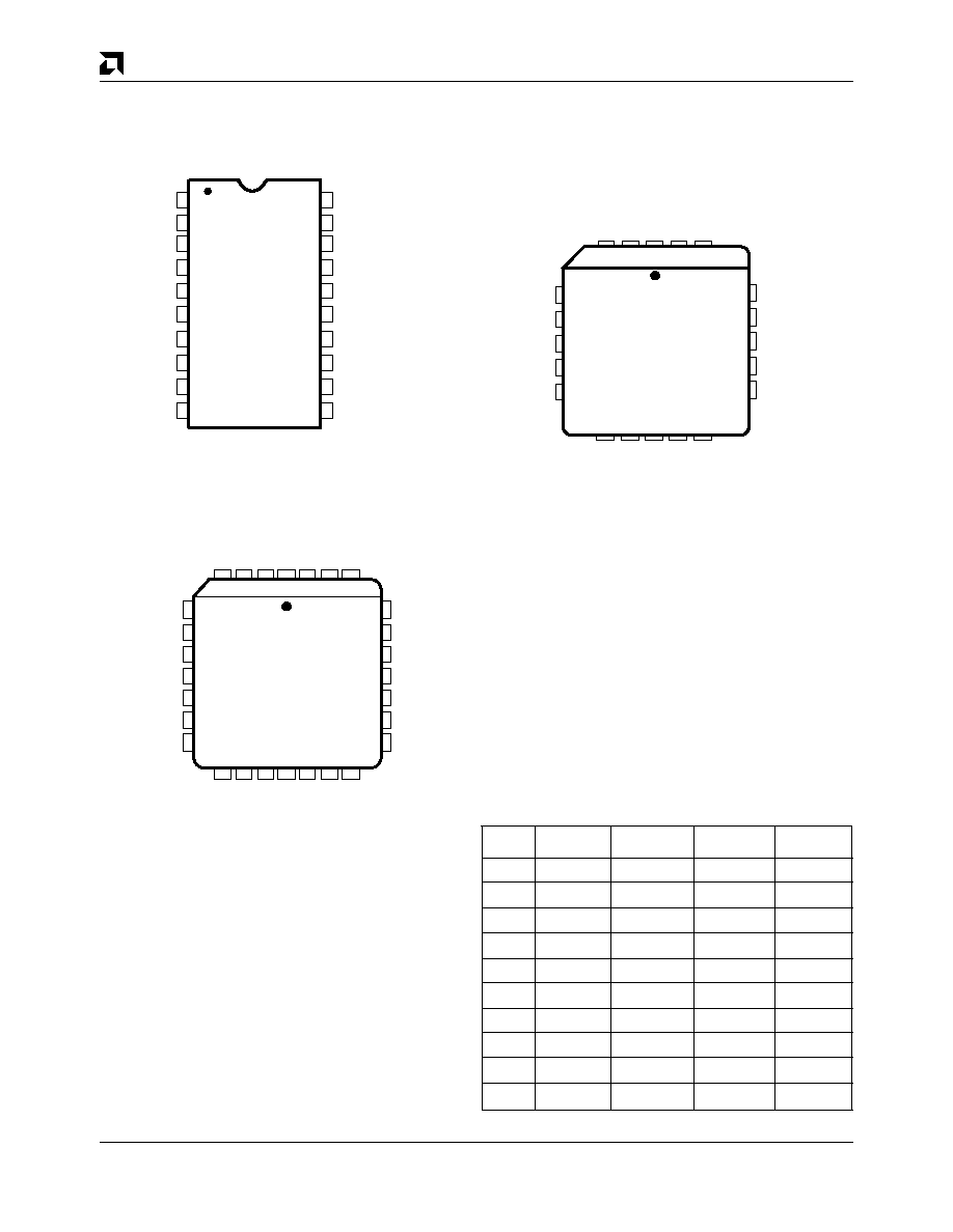
CONNECTION DIAGRAMS
Top View
1
2
3
4
28 27 26
25
5
24
23
22
21
20
19
18
17
16
15
6
7
8
9
10
11
12 13 14
I
8
GND
(Note 2)
(Note 3)
GND
(Note 4)
GND
I
1
(Note 1)
V
CC
(Note 10)
GND
(Note 9)
GND
(Note 8)
GND
(Note 7)
GND
(Note 5)
GND
(Note 6)
V
CC
I
5
I
6
I
7
I
4
I
3
I
2
1
20 19
18
17
16
15
14
2
3
4
5
6
7
8
9
10 11
12 13
I
3
I
4
I
5
I
6
I
7
(Note 9)
(Note 8)
(Note 7)
(Note 6)
(Note 5)
(Note 2)
(Note 3)
(Note 4)
GND
I
8
(Note 1)
V
CC
(Note 10)
I
1
I
2
16
14
12
13
19
Note
16L8
16R8
16R6
16R4
1
I
0
CLK
CLK
CLK
2
I
9
OE
OE
OE
3
O
1
O
1
I/O
1
I/O
1
4
I/O
2
O
2
O
2
I/O
2
5
I/O
3
O
3
O
3
O
3
6
I/O
4
O
4
O
4
O
4
7
I/O
5
O
5
O
5
O
5
8
I/O
6
O
6
O
6
O
6
9
I/O
7
O
7
O
7
I/O
7
10
O
8
O
8
I/O
8
I/O
8
PIN DESIGNATIONS
CLK
=
Clock
GND
=
Ground
I
=
Input
I/O
=
Input/Output
O
=
Output
OE
=
Output Enable
V
CC
=
Supply Voltage
DIP
20-Pin PLCC
(Note 1)
(Note 10)
I
1
I
2
I
3
I
4
I
5
I
6
I
7
GND
I
8
(Note 9)
(Note 8)
(Note 7)
(Note 5)
(Note 4)
(Note 3)
(Note 2)
V
CC
(Note 6)
28-Pin PLCC
Note:
Pin 1 is marked for orientation.
16492D-5
16492D-6
16492D-7
3
5
7
2
1
4
8
6
15
11
9
10
17
18
20

AMD
2-7
PAL16R8-4/5/7, D/2 (Com'l)
ORDERING INFORMATION
Commercial Products
AMD programmable logic products for commercial applications are available with several ordering options. The order number
(Valid Combination) is formed by a combination of:
Valid Combinations
Valid Combinations lists configurations planned
to be supported in volume for this device. Consult
the local AMD sales office to confirm availability of
specific valid combinations and to check on newly
released combinations.
PAL
16
R
8
-5
P C
FAMILY TYPE
PAL = Programmable Array Logic
NUMBER OF
ARRAY INPUTS
OUTPUT TYPE
R = Registered
L = Active-Low
Combinatorial
NUMBER OF OUTPUTS
SPEED
-4 = 4.5 ns t
PD
-5 = 5 ns t
PD
-7 = 7.5 ns t
PD
D = 10 ns t
PD
PACKAGE TYPE
P = 20-Pin Plastic DIP (PD 020)
J = 20-Pin Plastic Leaded Chip
Carrier (PL 020)
28-Pin Plastic Leaded Chip
Carrier for -4 (PL 028)
D = 20-Pin Ceramic DIP (CD 020)
OPERATING CONDITIONS
C = Commercial (0
�
C to +75
�
C)
OPTIONAL PROCESSING
Blank = Standard Processing
PAL16L8
-5PC, -5JC, -4JC
Valid Combinations
PAL16R8
PAL16R6
PAL16R4
PAL16L8-7
PAL16R8-7
PAL16R6-7
PAL16R4-7
PC, JC, DC
VERSION
Blank = First Revision
/2 = Second Revision
PAL16L8D/2
PAL16R8D/2
PAL16R6D/2
PAL16R4D/2
PC, JC

AMD
2-8
PAL16R8/B/B-2/A/B-4 (Com'l)
ORDERING INFORMATION
Commercial Products (MMI Marking Only)
h.
PACKAGE TYPE
N
= 20-Pin Plastic DIP
(PD 020)
NL = 20-Pin Plastic Leaded
Chip Carrier (PL 020)
J
= 20-Pin Ceramic DIP
(CD 020)
AMD programmable logic products for commercial applications are available with several ordering options. The order number
(Valid Combination) is formed by a combination of:
PAL16L8
Valid Combinations
Valid Combinations
Valid Combinations lists configurations planned
to be supported in volume for this device. Consult
the local AMD sales office to confirm availability of
specific valid combinations and to check on newly
released combinations.
Note: Marked with MMI logo.
PAL
16
R 8 B
C
N
PAL16R8
PAL16R6
PAL16R4
a.
FAMILY TYPE
PAL = Programmable Array Logic
b.
NUMBER OF
ARRAY INPUTS
c.
OUTPUT TYPE
R = Registered
L = Active-Low Combinatorial
d.
NUMBER OF OUTPUTS
SPEED
B = Very High Speed (15 ns�35 ns t
PD
)
A = High Speed (25 ns�35 ns t
PD
)
g.
OPERATING CONDITIONS
C
= Commercial (0
�
C to +75
�
C)
i.
OPTIONAL PROCESSING
Blank = Standard Processing
-2
f.
POWER
Blank = Full Power (155 mA�180 mA I
CC
)
-2
= Half Power (80 mA�90 mA I
CC
)
-4
= Quarter Power (55 mA I
CC
)
CN, CNL, CJ
B, B-2, A,
B-4

AMD
2-9
PAL16R8 Family
FUNCTIONAL DESCRIPTION
Standard 20-Pin PAL Family
The standard bipolar 20-pin PAL family devices have
common electrical characteristics and programming
procedures. Four different devices are available, includ-
ing both registered and combinatorial devices. All parts
are produced with a fuse link at each input to the AND
gate array, and connections may be selectively re-
moved by applying appropriate voltages to the circuit.
Utilizing an easily-implemented programming algo-
rithm, these products can be rapidly programmed to
any customized pattern. Extra test words are pre-
programmed during manufacturing to ensure extremely
high field programming yields, and provide extra test
paths to achieve excellent parametric correlation.
Pinouts
The PAL16R8 Family is available in the standard 20-pin
DIP and PLCC pinouts and the PAL16R8-4 Series is
available in the new 28-pin PLCC pinout. The 28-pin
PLCC pinout gives the designer the cleanest possible
signal with only 4.5 ns delay.
The PAL16R8-4 pinout has been designed to minimize
the noise that can be generated by high-speed signals.
Because of its inherently shorter leads, the PLCC pack-
age is the best package for use in high-speed designs.
The short leads and multiple ground signals reduce the
effective lead inductance, minimizing ground bounce.
Placing the ground pins between the outputs optimizes
the ground bounce protection, and also isolates the out-
puts from each other, eliminating cross-talk. This pinout
can reduce the effective propagation delay by as much
as 20% from a standard DIP pinout. Design files for
PAL16R8-4 Series devices are written as if the device
had a standard 20-pin DIP pinout for most design soft-
ware packages.
Variable Input/Output Pin Ratio
The registered devices have eight dedicated input lines,
and each combinatorial output is an I/O pin. The
PAL16L8 has ten dedicated input lines and six of the
eight combinatorial outputs are I/O pins. Buffers for de-
vice inputs have complementary outputs to provide
user-programmable input signal polarity. Unused input
pins should be tied to V
CC
or GND.
Programmable Three-State Outputs
Each output has a three-state output buffer with three-
state control. On combinatorial outputs, a product term
controls the buffer, allowing enable and disable to be a
function of any product of device inputs or output feed-
back. The combinatorial output provides a bidirectional
I/O pin and may be configured as a dedicated input if the
output buffer is always disabled. On registered outputs,
an input pin controls the enabling of the three-state
outputs.
Registers with Feedback
Registered outputs are provided for data storage and
synchronization. Registers are composed of D-type
flip-flops that are loaded on the LOW-to-HIGH transition
of the clock input.
Register Preload
The register on the AMD marked 16R8, 16R6, and 16R4
devices can be preloaded from the output pins to facili-
tate functional testing of complex state machine de-
signs. This feature allows direct loading of arbitrary
states, making it unnecessary to cycle through long test
vector sequences to reach a desired state. In addition,
transitions from illegal states can be verified by loading
illegal states and observing proper recovery.
Power-Up Reset
All flip-flops power-up to a logic LOW for predictable
system initialization. Outputs of the PAL16R8 Family
will be HIGH due to the active-low outputs. The V
CC
rise
must be monotonic and the reset delay time is 1000 ns
maximum.
Security Fuse
After programming and verification, a PAL16R8 Family
design can be secured by programming the security
fuse. Once programmed, this fuse defeats readback of
the internal programmed pattern by a device program-
mer, securing proprietary designs from competitors.
When the security fuse is programmed, the array will
read as if every fuse is programmed.
Quality and Testability
The PAL16R8 Family offers a very high level of built-in
quality. Extra programmable fuses provide a means of
verifying performance of all AC and DC parameters. In
addition, this verifies complete programmability and
functionality of the device to provide the highest pro-
gramming yields and post-programming functional
yields in the industry.
Technology
The PAL16R8-5, -7 and D/2 are fabricated with AMD's
oxide isolated bipolar process. The array connections
are formed with highly reliable PtSi fuses. The
PAL16R8B, B-2, A and B-4 series are fabricated with
AMD's advanced trench-isolated bipolar process. The
array connections are formed with proven TiW fuses for
reliable operation. These processes reduce parasitic
capacitances and minimum geometries to provide
higher performance.

AMD
2-10
PAL16R8 Family
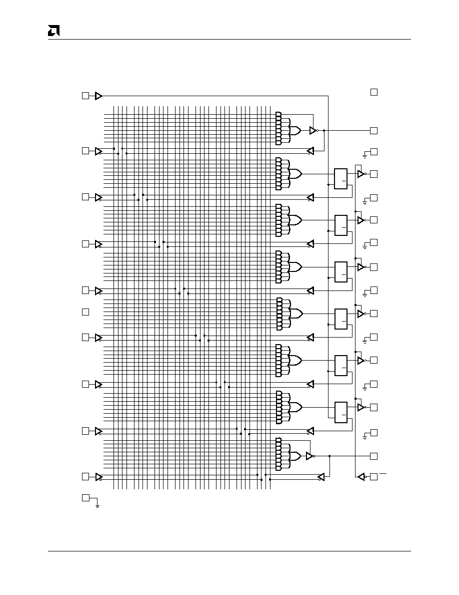
LOGIC DIAGRAM
DIP and 20-Pin PLCC (28-Pin PLCC) Pinouts
16492D-8
0 3 4 7 8 11
12 15
16 19
20 23
24 27
28 31
0
7
0 3 4 7 8 11
12 15
16 19
20 23
24 27
28 31
8
15
16
23
24
31
32
39
40
47
48
55
56
63
I0
I1
I3
I 4
I5
I6
I7
I8
I2
O8
I/O7
I/O6
I/O5
I/O4
I/O3
I/O2
O1
11 I9
GND
VCC
1
2
3
4
5
6
7
8
9
12
13
14
16
17
18
19
(24)
(25)
(26)
(27)
(28)
VCC
(1)
(2)
(3)
(4)
(5)
(6)
(22)
(21)
(20)
(18)
(16)
(14)
(12)
(10)
(8)
(7)
GND
(19)
GND
(17)
GND
(15)
GND
15
(13)
GND
(11)
GND
(9)
GND
(23)
20
16L8-5 (-4)
10
16L8 (-4)

AMD
2-11
PAL16R8 Family
LOGIC DIAGRAM
DIP and 20-Pin PLCC (28-Pin PLCC) Pinouts
16492D-9
0 3 4 7 8 11
12 15
16 19
20 23
24 27
28 31
0
7
0 3 4 7 8 11
12 15
16 19
20 23
24 27
28 31
8
15
16
23
24
31
32
39
40
47
48
55
56
63
16R8-5 (-4)
2
3
4
5
6
7
8
9
1
18
D Q
Q
19
17
16
15
14
13
12
11
O8
O7
O6
O5
O4
O3
O2
O1
OE
V
CLK
I1
I2
I3
I4
I5
I6
I7
I8
D Q
Q
V
D Q
Q
V
D Q
Q
V
D Q
Q
V
D Q
Q
V
D Q
Q
V
D Q
Q
V
GND
VCC
(21)
GND
(23)
(22)
(20)
(17)
GND
(18)
(16)
(15)
GND
(14)
GND
(11)
(12)
GND
(13)
(10)
GND
(9)
(8)
(7)
(6)
(5)
(4)
(3)
(2)
VCC
(1)
(28)
(27)
(26)
(25)
(24)
(19)
GND
10
20
16R8 (-4)
AMD
2-12
PAL16R8 Family
LOGIC DIAGRAM
DIP and 20-Pin PLCC (28-Pin PLCC) Pinouts
0 3 4 7 8 11
12 15
16 19
20 23
24 27
28 31
0
7
0 3 4 7 8 11
12 15
16 19
20 23
24 27
28 31
8
15
16
23
24
31
32
39
40
47
48
55
56
63
16R6-5 (-4)
2
3
4
6
7
9
10
1
18
D Q
Q
19
17
16
15
14
13
12
11
I/O8
O7
O6
O5
O4
O3
O2
I/O1
OE
V
CLK
I1
I2
I3
I4
I5
I6
I7
I8
D Q
Q
V
D Q
Q
V
D Q
Q
V
D Q
Q
V
D Q
Q
V
GND
(22)
VCC
(23)
(17)
GND
(21)
GND
(20)
(18)
(19)
GND
(16)
(15)
GND
(14)
(13)
GND
(12)
(11)
GND
(10)
(9)
GND
(8)
(7)
VCC
(1)
(28)
5
(6)
(5)
(4)
(3)
(2)
(27)
(26)
(25)
(24)
8
20
16R6 (-4)
16492D-10

AMD
2-13
PAL16R8 Family
LOGIC DIAGRAM
DIP and 20-Pin PLCC (28-Pin PLCC) Pinouts
0 3 4 7 8 11
12 15
16 19
20 23
24 27
28 31
0
7
0 3 4 7 8 11
12 15
16 19
20 23
24 27
28 31
8
15
16
23
24
31
32
39
40
47
48
55
56
63
16R4-5 (-4)
1
CLK
I1
I3
I4
I5
I6
I7
I8
I2
I/O8
I/O7
O6
O5
O4
O3
I/O2
I/O1
OE
GND
VCC
2
3
4
5
6
7
8
9
11
12
13
14
15
16
17
18
19
D Q
Q
V
D Q
Q
V
D Q
Q
V
D Q
Q
V
(6)
(19)
GND
(23)
(22)
(20)
(21)
GND
(18)
(17)
GND
(16)
(14)
GND
(15)
GND
(13)
(12)
GND
(11)
(10)
GND
(9)
(8)
(7)
(5)
(4)
(3)
(2)
VCC
(1)
(28)
(27)
(26)
(25)
(24)
10
20
16R4 (-4)
16492D-11
AMD
2-14
PAL16R8-4/5 (Com'l)
Parameter
Symbol
Parameter Description
Test Conditions
Min
Max
Unit
V
OH
Output HIGH Voltage
I
OH
= �3.2 mA
V
IN
= V
IH
or V
IL
2.4
V
V
CC
= Min
V
OL
Output LOW Voltage
I
OL
= 24 mA
V
IN
= V
IH
or V
IL
0.5
V
V
CC
= Min
V
IH
Input HIGH Voltage
Guaranteed Input Logical HIGH
2.0
V
Voltage for all Inputs (Note 1)
V
IL
Input LOW Voltage
Guaranteed Input Logical LOW
0.8
V
Voltage for all Inputs (Note 1)
V
I
Input Clamp Voltage
I
IN
= �18 mA, V
CC
= Min
�1.2
V
I
IH
Input HIGH Current
V
IN
= 2.7 V, V
CC
= Max (Note 2)
25
�
A
I
IL
Input LOW Current
V
IN
= 0.4 V, V
CC
= Max (Note 2)
�250
�
A
I
I
Maximum Input Current
V
IN
= 5.5 V, V
CC
= Max
1
mA
I
OZH
Off-State Output Leakage
V
OUT
= 2.7 V, V
CC
= Max
100
�
A
Current HIGH
V
IN
= V
IH
or V
IL
(Note 2)
I
OZL
Off-State Output Leakage
V
OUT
= 0.4 V, V
CC
= Max
�100
�
A
Current LOW
V
IN
= V
IH
or V
IL
(Note 2)
I
SC
Output Short-Circuit Current
V
OUT
= 0.5 V, V
CC
= Max (Note 3)
�30
�130
mA
I
CC
Supply Current
V
IN
= 0 V, Outputs Open (I
OUT
= 0 mA)
210
mA
V
CC
= Max
DC CHARACTERISTICS over COMMERCIAL operating ranges unless otherwise
specified
ABSOLUTE MAXIMUM RATINGS
Ambient Temperature with
Power Applied
�65
�
C to +150
�
C
. . . . . . . . . . . . . . .
Storage Temperature
�55
�
C to +125
�
C
. . . . . . . . . .
Supply Voltage with
Respect to Ground
�0.5 V to + 7.0 V
. . . . . . . . . . . . .
DC Input Voltage
�1.2 V to V
CC
+ 0.5 V
. . . . . . . . . .
DC Input Current
�30 mA to + 5 mA
. . . . . . . . . . . . .
DC Output or I/O Pin
Voltage
�0.5 V to V
CC
+ 0.5 V
. . . . . . . . . . . . . . . . . .
Static Discharge Voltage
2001 V
. . . . . . . . . . . . . . .
Stresses above those listed under Absolute Maximum Rat-
ings may cause permanent device failure. Functionality at or
above these limits is not implied. Exposure to Absolute Maxi-
mum Ratings for extended periods may affect device reliabil-
ity. Programming conditions may differ.
OPERATING RANGES
Commercial (C) Devices
Ambient Temperature (T
A
)
Operating in Free Air
0
�
C to +75
�
C
. . . . . . . . . . . . . . .
Supply Voltage (V
CC
)
with Respect to Ground
+4.75 V to +5.25 V
. . . . . . . . .
Operating ranges define those limits between which the func-
tionality of the device is guaranteed.
Notes:
1. These are absolute values with respect to device ground and all overshoots due to system and/or tester noise are included.
2. I/O pin leakage is the worst case of I
IL
and I
OZL
(or I
IH
and I
OZH
).
3. Not more than one output should be tested at a time. Duration of the short-circuit should not exceed one second. V
OUT
= 0.5 V
has been chosen to avoid test problems caused by tester ground degradation.

AMD
2-15
PAL16R8-4/5 (Com'l)
Parameter
Symbol
Parameter Description
Test Conditions
Typ
Unit
C
IN
Input Capacitance
V
IN
= 2.0 V
V
CC
= 5.0 V
8
5
C
OUT
Output Capacitance
V
OUT
= 2.0 V
f = 1 MHz
8
Note:
1. These parameters are not 100% tested, but are evaluated at initial characterization and at any time the design is modified
where capacitance may be affected.
Parameter
Min
Min
Symbol
Parameter Description
(Note 3)
Max
(Note 3)
Max
Unit
t
PD
Input or Feedback to Combinatorial Output
1
5
1
4.5
ns
t
S
Setup Time from Input or Feedback to Clock
4.5
4.5
ns
t
H
Hold Time
0
0
ns
t
CO
Clock to Output
1
4.0
1
3.5
ns
t
SKEWR
Skew Between Registered Outputs (Note 4)
1
0.5
ns
t
WL
LOW
4
4
ns
t
WH
HIGH
4
4
ns
External Feedback
1/(t
S
+ t
CO
)
117
125
MHz
Internal Feedback
1/(t
S
+ t
CF
)
125
125
MHz
(f
CNT
)
(Note 6)
No Feedback
1/(t
WH
+ t
WL
)
125
125
MHz
t
PZX
OE
to Output Enable
1
6.5
1
6.5
ns
t
PXZ
OE
to Output Disable
1
5
1
5
ns
t
EA
Input to Output Enable Using
2
6.5
2
6.5
ns
Product Term Control
t
ER
Input to Output Disable Using
2
5
2
5
ns
Product Term Control
CAPACITANCE (Note 1)
SWITCHING CHARACTERISTICS over COMMERCIAL operating ranges (Note 2)
T
A
=
25
�
C
pF
Clock Width
Maximum
Frequency
(Note 5)
f
MAX
-5
-4
Notes:
2. See Switching Test Circuit for test conditions.
3. Output delay minimums for t
PD
, t
CO
, t
PZX
, t
PXZ
, t
EA
, and t
ER
are defined under best case conditions. Future process improve-
ments may alter these values; therefore, minimum values are recommended for simulation purposes only.
4. Skew testing takes into account pattern and switching direction differences between outputs.
5. These parameters are not 100% tested, but are calculated at initial characterization and at any time the design is modified
where the frequency may be affected.
6. t
CF
is a calculated value and is not guaranteed. t
CF
can be found using the following equation:
t
CF
= 1/f
MAX
(internal feedback) � t
S
.
16R8, 16R6,
16R4
16L8, 16R6,
16R4
16L8, 16R8,
16R4
CLK,
OE
I
1
�I
8

AMD
2-16
PAL16R8-7 (Com'l)
ABSOLUTE MAXIMUM RATINGS
Storage Temperature
�65
�
C to +150
�
C
. . . . . . . . . . .
Ambient Temperature with
Power Applied
�55
�
C to +125
�
C
. . . . . . . . . . . . . . . . .
Supply Voltage with
Respect to Ground
�0.5 V to + 7.0 V
. . . . . . . . . . . . .
DC Input Voltage
�1.2 V to + 7.0 V
. . . . . . . . . . . . . . .
DC Input Current
�30 mA to + 5 mA
. . . . . . . . . . . . . .
DC Output or I/O Pin
Voltage
�0.5 V to V
CC
+ 0.5 V
. . . . . . . . . . . . . . . . . .
Static Discharge Voltage
2001 V
. . . . . . . . . . . . . . . . .
Stresses above those listed under Absolute Maximum Rat-
ings may cause permanent device failure. Functionality at or
above these limits is not implied. Exposure to Absolute Maxi-
mum Ratings for extended periods may affect device reliabil-
ity. Programming conditions may differ.
OPERATING RANGES
Commercial (C) Devices
Ambient Temperature (T
A
)
Operating in Free Air
0
�
C to +75
�
C
. . . . . . . . . . . . . .
Supply Voltage (V
CC
)
with Respect to Ground
+4.75 V to +5.25 V
. . . . . . . .
Operating ranges define those limits between which the func-
tionality of the device is guaranteed.
DC CHARACTERISTICS over COMMERCIAL operating ranges unless otherwise
specified
Parameter
Symbol
Parameter Description
Test Conditions
Min
Max
Unit
V
OH
Output HIGH Voltage
I
OH
= �3.2 mA
V
IN
= V
IH
or V
IL
2.4
V
V
CC
= Min
V
OL
Output LOW Voltage
I
OL
= 24 mA
V
IN
= V
IH
or V
IL
0.5
V
V
CC
= Min
V
IH
Input HIGH Voltage
Guaranteed Input Logical HIGH
2.0
V
Voltage for all Inputs (Note 1)
V
IL
Input LOW Voltage
Guaranteed Input Logical LOW
0.8
V
Voltage for all Inputs (Note 1)
V
I
Input Clamp Voltage
I
IN
= �18 mA, V
CC
= Min
�1.2
V
I
IH
Input HIGH Current
V
IN
= 2.7 V, V
CC
= Max (Note 2)
25
�
A
I
IL
Input LOW Current
V
IN
= 0.4 V, V
CC
= Max (Note 2)
�250
�
A
I
I
Maximum Input Current
V
IN
= 5.5 V, V
CC
= Max
1
mA
I
OZH
Off-State Output Leakage
V
OUT
= 2.7 V, V
CC
= Max
100
�
A
Current HIGH
V
IN
= V
IH
or V
IL
(Note 2)
I
OZL
Off-State Output Leakage
V
OUT
= 0.4 V, V
CC
= Max
�100
�
A
Current LOW
V
IN
= V
IH
or V
IL
(Note 2)
I
SC
Output Short-Circuit Current
V
OUT
= 0.5 V, V
CC
= Max (Note 3)
�30
�130
mA
I
CC
Supply Current
V
IN
= 0 V, Outputs Open (I
OUT
= 0 mA)
180
mA
V
CC
= Max
Notes:
1. These are absolute values with respect to device ground and all overshoots due to system and/or tester noise are included.
2. I/O pin leakage is the worst case of I
IL
and I
OZL
(or I
IH
and I
OZH
).
3. Not more than one output should be tested at a time. Duration of the short-circuit should not exceed one second. V
OUT
= 0.5 V
has been chosen to avoid test problems caused by tester ground degradation.

AMD
2-17
PAL16R8-7 (Com'l)
CAPACITANCE (Note 1)
Parameter
Symbol
Parameter Description
Test Conditions
Typ
Unit
C
IN
Input Capacitance
V
IN
= 2.0 V
5
C
OUT
Output Capacitance
V
OUT
= 2.0 V
8
V
CC
= 5.0 V
T
A
= 25
�
C
f = 1 MHz
pF
Note:
1. These parameters are not 100% tested, but are evaluated at initial characterization and at any time the design is modified
where capacitance may be affected.
SWITCHING CHARACTERISTICS over COMMERCIAL operating ranges (Note 2)
Parameter
Min
Symbol
Parameter Description
(Note 3)
Max
Unit
16L8, 16R6,
3
7.5
16R4
3
7
t
S
Setup Time from Input or Feedback to Clock
7
ns
t
H
Hold Time
0
ns
t
CO
Clock to Output
1
6.5
ns
t
SKEW
Skew Between Registered Outputs (Note 4)
16R8, 16R6,
1
ns
t
WL
LOW
16R4
5
ns
t
WH
HIGH
5
ns
External Feedback
1/(t
S
+ t
CO
)
74
MHz
f
MAX
Internal Feedback
1/(t
S
+ t
CF
) 100
MHz
(f
CNT
)
(Note 6)
No Feedback
1/(t
WH
+ t
WL
)
100
MHz
t
PZX
OE
to Output Enable
1
8
ns
t
PXZ
OE
to Output Disable
1
8
ns
t
EA
Input to Output Enable Using Product Term Control
16L8, 16R6,
3
10
ns
t
ER
Input to Output Disable Using Product Term Control
16R4
3
10
ns
ns
Maximum
Frequency
(Note 5)
Clock Width
t
PD
Input or Feedback to
Combinatorial Output
1 Output Switching
Notes:
2. See Switching Test Circuit for test conditions.
3. Output delay minimums for t
PD
, t
CO
, t
PZX
, t
PXZ
, t
EA
, and t
ER
are defined under best case conditions. Future process improve-
ments may alter these values; therefore, minimum values are recommended for simulation purposes only.
4. Skew is measured with all outputs switching in the same direction.
5. These parameters are not 100% tested, but are calculated at initial characterization and at any time the design is modified
where the frequency may be affected.
6. t
CF
is a calculated value and is not guaranteed. t
CF
can be found using the following equation:
t
CF
= 1/f
MAX
(internal feedback) � t
S
.

AMD
2-18
PAL16R8D/2 (Com'l)
ABSOLUTE MAXIMUM RATINGS
Storage Temperature
�65
�
C to +150
�
C
. . . . . . . . . . .
Ambient Temperature with
Power Applied
�55
�
C to +125
�
C
. . . . . . . . . . . . . . . . .
Supply Voltage with
Respect to Ground
�0.5 V to + 7.0 V
. . . . . . . . . . . . .
DC Input Voltage
�1.5 V to + 5.5 V
. . . . . . . . . . . . . . .
DC Output or I/O Pin Voltage
�0.5 V to + 5.5 V
. . . . .
Static Discharge Voltage
2001 V
. . . . . . . . . . . . . . . . .
Stresses above those listed under Absolute Maximum Rat-
ings may cause permanent device failure. Functionality at or
above these limits is not implied. Exposure to Absolute Maxi-
mum Ratings for extended periods may affect device reliabil-
ity. Programming conditions may differ.
OPERATING RANGES
Commercial (C) Devices
Ambient Temperature (T
A
)
Operating in Free Air
0
�
C to +75
�
C
. . . . . . . . . . . . . .
Supply Voltage (V
CC
)
with Respect to Ground
+4.75 V to +5.25 V
. . . . . . . .
Operating ranges define those limits between which the func-
tionality of the device is guaranteed.
DC CHARACTERISTICS over COMMERCIAL operating ranges unless otherwise
specified
Parameter
Symbol
Parameter Description
Test Conditions
Min
Max
Unit
V
OH
Output HIGH Voltage
I
OH
= �3.2 mA
V
IN
= V
IH
or V
IL
2.4
V
V
CC
= Min
V
OL
Output LOW Voltage
I
OL
= 24 mA
V
IN
= V
IH
or V
IL
0.5
V
V
CC
= Min
V
IH
Input HIGH Voltage
Guaranteed Input Logical HIGH
2.0
V
Voltage for all Inputs (Note 1)
V
IL
Input LOW Voltage
Guaranteed Input Logical LOW
0.8
V
Voltage for all Inputs (Note 1)
V
I
Input Clamp Voltage
I
IN
= �18 mA, V
CC
= Min
�1.5
V
I
IH
Input HIGH Current
V
IN
= 2.4 V, V
CC
= Max (Note 2)
25
�
A
I
IL
Input LOW Current
V
IN
= 0.4 V, V
CC
= Max (Note 2)
�250
�
A
I
I
Maximum Input Current
V
IN
= 5.5 V, V
CC
= Max
100
�
A
I
OZH
Off-State Output Leakage
V
OUT
= 2.4 V, V
CC
= Max
100
�
A
Current HIGH
V
IN
= V
IH
or V
IL
(Note 2)
I
OZL
Off-State Output Leakage
V
OUT
= 0.4 V, V
CC
= Max
�100
�
A
Current LOW
V
IN
= V
IH
or V
IL
(Note 2)
I
SC
Output Short-Circuit Current
V
OUT
= 0.5 V, V
CC
= Max (Note 3)
�30
�130
mA
I
CC
Supply Current
V
IN
= 0 V, Outputs Open (I
OUT
= 0 mA)
180
mA
V
CC
= Max
Notes:
1. These are absolute values with respect to device ground and all overshoots due to system and/or tester noise are included.
2. I/O pin leakage is the worst case of I
IL
and I
OZL
(or I
IH
and I
OZH
).
3. Not more than one output should be tested at a time. Duration of the short-circuit should not exceed one second.
V
OUT
= 0.5 V has been chosen to avoid test problems caused by tester ground degradation.

AMD
2-19
PAL16R8D/2 (Com'l)
CAPACITANCE (Note 1)
Parameter
Symbol
Parameter Description
Test Conditions
Typ
Unit
C
IN
Input Capacitance
V
IN
= 2.0 V
V
CC
= 5.0 V
5
C
OUT
Output Capacitance
V
OUT
= 2.0 V
f = 1 MHz
8
Note:
1. These parameters are not 100% tested, but are evaluated at initial characterization and at any time the design is modified
where capacitance may be affected.
T
A
= 25
�
C
pF
SWITCHING CHARACTERISTICS over COMMERCIAL operating ranges (Note 2)
Parameter
Min
Symbol
Parameter Description
(Note 3)
Max
Unit
t
PD
Input or Feedback to Combinatorial Output
16L8, 16R6,
3
10
ns
16R4
t
S
Setup Time from Input or Feedback to Clock
10
ns
t
H
Hold Time
0
ns
t
CO
Clock to Output
3
7
ns
t
WL
Clock Width
LOW
8
ns
t
WH
HIGH
16R8, 16R6,
8
ns
External Feedback
1/(t
S
+ t
CO
)
16R4
58.8
MHz
f
MAX
Internal Feedback
1/(t
S
+ t
CF
) 60
MHz
(f
CNT
)
(Note 5)
No Feedback
1/(t
WH
+ t
WL
)
62.5
MHz
t
PZX
OE
to Output Enable
2
10
ns
t
PXZ
OE
to Output Disable
2
10
ns
t
EA
Input to Output Enable Using Product Term Control
16L8, 16R6,
3
10
ns
t
ER
Input to Output Disable Using Product Term Control
16R4
3
10
ns
Maximum
Frequency
(Note 4)
Notes:
2. See Switching Test Circuit for test conditions.
3. Output delay minimums for t
PD
, t
CO
, t
PZX
, t
PXZ
, t
EA
, and t
ER
are defined under best case conditions. Future process improve-
ments may alter these values; therefore, minimum values are recommended for simulation purposes only.
4. These parameters are not 100% tested, but are calculated at initial characterization and at any time the design is modified
where the frequency may be affected.
5. t
CF
is a calculated value and is not guaranteed. t
CF
can be found using the following equation:
t
CF
= 1/f
MAX
(internal feedback) � t
S
.

AMD
2-20
PAL16R8B (Com'l)
ABSOLUTE MAXIMUM RATINGS
Storage Temperature
�65
�
C to +150
�
C
. . . . . . . . . . .
Ambient Temperature with
Power Applied
�55
�
C to +125
�
C
. . . . . . . . . . . . . . . . .
Supply Voltage with
Respect to Ground
�0.5 V to +7.0 V
. . . . . . . . . . . . .
DC Input Voltage
�1.5 V to V
CC
+ 0.5 V
. . . . . . . . . . .
DC Output or I/O Pin
Voltage
�0.5 V to V
CC
+ 0.5 V
. . . . . . . . . . . . . . . . . .
Stresses above those listed under Absolute Maximum Rat-
ings may cause permanent device failure. Functionality at or
above these limits is not implied. Exposure to Absolute Maxi-
mum Ratings for extended periods may affect device reliabil-
ity. Programming conditions may differ.
OPERATING RANGES
Commercial (C) Devices
Ambient Temperature (T
A
)
Operating in Free Air
0
�
C to +75
�
C
. . . . . . . . . . . . . .
Supply Voltage (V
CC
)
with Respect to Ground
+4.75 V to +5.25 V
. . . . . . . .
Operating ranges define those limits between which the func-
tionality of the device is guaranteed.
DC CHARACTERISTICS over COMMERCIAL operating ranges unless otherwise
specified
Parameter
Symbol
Parameter Description
Test Conditions
Min
Max
Unit
V
OH
Output HIGH Voltage
I
OH
= �3.2 mA
V
IN
= V
IH
or V
IL
2.4
V
V
CC
= Min
V
OL
Output LOW Voltage
I
OL
= 24 mA
V
IN
= V
IH
or V
IL
0.5
V
V
CC
= Min
V
IH
Input HIGH Voltage
Guaranteed Input Logical HIGH
2.0
V
Voltage for all Inputs (Note 1)
V
IL
Input LOW Voltage
Guaranteed Input Logical LOW
0.8
V
Voltage for all Inputs (Note 1)
V
I
Input Clamp Voltage
I
IN
= �18 mA, V
CC
= Min
�1.2
V
I
IH
Input HIGH Current
V
IN
= 2.4 V, V
CC
= Max (Note 2)
25
�
A
I
IL
Input LOW Current
V
IN
= 0.4 V, V
CC
= Max (Note 2)
�250
�
A
I
I
Maximum Input Current
V
IN
= 5.5 V, V
CC
= Max
100
�
A
I
OZH
Off-State Output Leakage
V
OUT
= 2.4 V, V
CC
= Max
100
�
A
Current HIGH
V
IN
= V
IH
or V
IL
(Note 2)
I
OZL
Off-State Output Leakage
V
OUT
= 0.4 V, V
CC
= Max
�100
�
A
Current LOW
V
IN
= V
IH
or V
IL
(Note 2)
I
SC
Output Short-Circuit Current
V
OUT
= 0.5 V, V
CC
= Max (Note 3)
�30
�130
mA
I
CC
Supply Current
V
IN
= 0 V, Outputs Open (I
OUT
= 0 mA)
180
mA
V
CC
= Max
Notes:
1. These are absolute values with respect to device ground and all overshoots due to system and/or tester noise are included.
2. I/O pin leakage is the worst case of I
IL
and I
OZL
(or I
IH
and I
OZH
).
3. Not more than one output should be tested at a time. Duration of the short-circuit should not exceed one second.
V
OUT
= 0.5 V has been chosen to avoid test problems caused by tester ground degradation.

AMD
2-21
PAL16R8B (Com'l)
CAPACITANCE (Note 1)
Parameter
Symbol
Parameter Description
Test Conditions
Typ
Unit
C
IN
Input Capacitance
V
IN
= 2.0 V
V
CC
= 5.0 V
8
C
OUT
Output Capacitance
V
OUT
= 2.0 V
f = 1 MHz
9
T
A
= 25
�
C
pF
Note:
1. These parameters are not 100% tested, but are evaluated at initial characterization and at any time the design is modified
where capacitance may be affected.
SWITCHING CHARACTERISTICS over COMMERCIAL operating ranges (Note 2)
Parameter
Symbol
Parameter Description
Min
Max
Unit
t
PD
Input or Feedback to Combinatorial Output
16L8, 16R6,
15
ns
16R4
t
S
Setup Time from Input or Feedback to Clock
15
ns
t
H
Hold Time
0
ns
t
CO
Clock to Output or Feedback
12
ns
t
WL
Clock Width
LOW
10
ns
t
WH
HIGH
10
ns
Maximum
External Feedback
1/(t
S
+ t
CO
)
37
MHz
f
MAX
Frequency
(Note 3)
No Feedback
1/(t
WH
+ t
WL
)
50
MHz
t
PZX
OE
to Output Enable
15
ns
t
PXZ
OE
to Output Disable
15
ns
t
EA
Input to Output Enable Using Product Term Control
15
ns
t
ER
Input to Output Disable Using Product Term Control
15
ns
16R8, 16R6,
16R4
16R8, 16R6,
16R4
Notes:
2. See Switching Test Circuit for test conditions.
3. These parameters are not 100% tested, but are evaluated at initial characterization and at any time the design is modified
where capacitance may be affected.
AMD
2-22
PAL16R8B-2 (Com'l)
ABSOLUTE MAXIMUM RATINGS
Storage Temperature
�65
�
C to +150
�
C
. . . . . . . . . . .
Ambient Temperature with
Power Applied
�55
�
C to +125
�
C
. . . . . . . . . . . . . . . . .
Supply Voltage with
Respect to Ground
�0.5 V to +7.0 V
. . . . . . . . . . . . .
DC Input Voltage
�1.5 V to V
CC
+ 0.5 V
. . . . . . . . . . .
DC Output or I/O Pin
Voltage
�0.5 V to V
CC
+ 0.5 V
. . . . . . . . . . . . . . . . . .
Stresses above those listed under Absolute Maximum Rat-
ings may cause permanent device failure. Functionality at or
above these limits is not implied. Exposure to Absolute Maxi-
mum Ratings for extended periods may affect device reliabil-
ity. Programming conditions may differ.
OPERATING RANGES
Commercial (C) Devices
Ambient Temperature (T
A
)
Operating in Free Air
0
�
C to +75
�
C
. . . . . . . . . . . . . .
Supply Voltage (V
CC
)
with Respect to Ground
+4.75 V to +5.25 V
. . . . . . . .
Operating ranges define those limits between which the func-
tionality of the device is guaranteed.
DC CHARACTERISTICS over COMMERCIAL operating ranges unless otherwise
specified
Parameter
Symbol
Parameter Description
Test Conditions
Min
Max
Unit
V
OH
Output HIGH Voltage
I
OH
= �3.2 mA
V
IN
= V
IH
or V
IL
2.4
V
V
CC
= Min
V
OL
Output LOW Voltage
I
OL
= 24 mA
V
IN
= V
IH
or V
IL
0.5
V
V
CC
= Min
V
IH
Input HIGH Voltage
Guaranteed Input Logical HIGH
2.0
V
Voltage for all Inputs (Note 1)
V
IL
Input LOW Voltage
Guaranteed Input Logical LOW
0.8
V
Voltage for all Inputs (Note 1)
V
I
Input Clamp Voltage
I
IN
= �18 mA, V
CC
= Min
�1.2
V
I
IH
Input HIGH Current
V
IN
= 2.7 V, V
CC
= Max (Note 2)
25
�
A
I
IL
Input LOW Current
V
IN
= 0.4 V, V
CC
= Max (Note 2)
�100
�
A
I
I
Maximum Input Current
V
IN
= 5.5 V, V
CC
= Max
100
�
A
I
OZH
Off-State Output Leakage
V
OUT
= 2.7 V, V
CC
= Max
100
�
A
Current HIGH
V
IN
= V
IH
or V
IL
(Note 2)
I
OZL
Off-State Output Leakage
V
OUT
= 0.4 V, V
CC
= Max
�100
�
A
Current LOW
V
IN
= V
IH
or V
IL
(Note 2)
I
SC
Output Short-Circuit Current
V
OUT
= 0.5 V, V
CC
= Max (Note 3)
�30
�130
mA
I
CC
Supply Current
V
IN
= 0 V, Outputs Open (I
OUT
= 0 mA)
90
mA
V
CC
= Max
Notes:
1. These are absolute values with respect to device ground and all overshoots due to system and/or tester noise are included.
2. I/O pin leakage is the worst case of I
IL
and I
OZL
(or I
IH
and I
OZH
).
3. Not more than one output should be tested at a time. Duration of the short-circuit should not exceed one second. V
OUT
= 0.5 V
has been chosen to avoid test problems caused by tester ground degradation.

AMD
2-23
PAL16R8B-2 (Com'l)
CAPACITANCE (Note 1)
Parameter
Symbol
Parameter Description
Test Conditions
Typ
Unit
C
IN
Input Capacitance
V
IN
= 2.0 V
V
CC
= 5.0 V
7
C
OUT
Output Capacitance
V
OUT
= 2.0 V
f = 1 MHz
7
T
A
= 25
�
C
pF
Note:
1. These parameters are not 100% tested, but are evaluated at initial characterization and at any time the design is modified
where capacitance may be affected.
SWITCHING CHARACTERISTICS over COMMERCIAL operating ranges (Note 2)
Parameter
Symbol
Parameter Description
Min
Max
Unit
t
PD
Input or Feedback to Combinatorial Output
16L8, 16R6,
25
ns
16R4
t
S
Setup Time from Input or Feedback to Clock
25
ns
t
H
Hold Time
0
ns
t
CO
Clock to Output
15
ns
t
WL
Clock Width
LOW
15
ns
t
WH
HIGH
15
ns
External Feedback
1/(t
S
+ t
CO
)
25
MHz
f
MAX
Internal Feedback
1/(t
S
+ t
CF
)
28.5
MHz
(f
CNT
)
(Note 5)
No Feedback
1/(t
WH
+ t
WL
)
33
MHz
t
PZX
OE
to Output Enable
20
ns
t
PXZ
OE
to Output Disable
20
ns
t
EA
Input to Output Enable Using Product Term Control
25
ns
t
ER
Input to Output Disable Using Product Term Control
25
ns
Maximum
Frequency
(Note 4)
16R8, 16R6,
16R4
16R8, 16R6,
16R4
Notes:
2. See Switching Test Circuit for test conditions.
3. Calculated from measured f
MAX
internal.
4. These parameters are not 100% tested, but are calculated at initial characterization and at any time the design is modified
where frequency may be affected.
5. t
CF
is a calculated value and is not guaranteed. t
CF
can be found using the following equation:
t
CF
= 1/f
MAX
(internal feedback) � t
S
.

AMD
2-24
PAL16R8A (Com'l)
ABSOLUTE MAXIMUM RATINGS
Storage Temperature
�65
�
C to +150
�
C
. . . . . . . . . . .
Ambient Temperature with
Power Applied
�55
�
C to +125
�
C
. . . . . . . . . . . . . . . . .
Supply Voltage with
Respect to Ground
�0.5 V to + 7.0 V
. . . . . . . . . . . . .
DC Input Voltage
�1.5 V to V
CC
+ 0.5 V
. . . . . . . . . . .
DC Output or I/O Pin
Voltage
�0.5 V to V
CC
+ 0.5 V
. . . . . . . . . . . . . . . . . .
Stresses above those listed under Absolute Maximum Rat-
ings may cause permanent device failure. Functionality at or
above these limits is not implied. Exposure to Absolute Maxi-
mum Ratings for extended periods may affect device reliabil-
ity. Programming conditions may differ.
OPERATING RANGES
Commercial (C) Devices
Ambient Temperature (T
A
)
Operating in Free Air
0
�
C to +75
�
C
. . . . . . . . . . . . . .
Supply Voltage (V
CC
)
with Respect to Ground
+4.75 V to +5.25 V
. . . . . . . .
Operating ranges define those limits between which the func-
tionality of the device is guaranteed.
DC CHARACTERISTICS over COMMERCIAL operating ranges unless otherwise
specified
Parameter
Symbol
Parameter Description
Test Conditions
Min
Max
Unit
V
OH
Output HIGH Voltage
I
OH
= �3.2 mA
V
IN
= V
IH
or V
IL
2.4
V
V
CC
= Min
V
OL
Output LOW Voltage
I
OL
= 24 mA
V
IN
= V
IH
or V
IL
0.5
V
V
CC
= Min
V
IH
Input HIGH Voltage
Guaranteed Input Logical HIGH
2.0
V
Voltage for all Inputs (Note 1)
V
IL
Input LOW Voltage
Guaranteed Input Logical LOW
0.8
V
Voltage for all Inputs (Note 1)
V
I
Input Clamp Voltage
I
IN
= �18 mA, V
CC
= Min
�1.2
V
I
IH
Input HIGH Current
V
IN
= 2.7 V, V
CC
= Max (Note 2)
25
�
A
I
IL
Input LOW Current
V
IN
= 0.4 V, V
CC
= Max (Note 2)
�250
�
A
I
I
Maximum Input Current
V
IN
= 5.5 V, V
CC
= Max
100
�
A
I
OZH
Off-State Output Leakage
V
OUT
= 2.7 V, V
CC
= Max
100
�
A
Current HIGH
V
IN
= V
IH
or V
IL
(Note 2)
I
OZL
Off-State Output Leakage
V
OUT
= 0.4 V, V
CC
= Max
�100
�
A
Current LOW
V
IN
= V
IH
or V
IL
(Note 2)
I
SC
Output Short-Circuit Current
V
OUT
= 0.5 V, V
CC
= Max (Note 3)
�30
�130
mA
16L8
V
IN
= 0 V, Outputs Open (I
OUT
= 0 mA)
155
mA
16R8/6/4
V
CC
= Max
180
I
CC
Supply Current
Notes:
1. These are absolute values with respect to device ground and all overshoots due to system and/or tester noise are included.
2. I/O pin leakage is the worst case of I
IL
and I
OZL
(or I
IH
and I
OZH
).
3. Not more than one output should be tested at a time. Duration of the short-circuit should not exceed one second. V
CC
= 0.5 V
has been chosen to avoid test problems caused by tester ground degradation.

AMD
2-25
PAL16R8A (Com'l)
CAPACITANCE (Note 1)
Parameter
Symbol
Parameter Description
Test Conditions
Typ
Unit
C
IN
Input Capacitance
V
IN
= 2.0 V
V
CC
= 5.0 V
7
C
OUT
Output Capacitance
V
OUT
= 2.0 V
f = 1 MHz
7
T
A
= 25
�
C
pF
Note:
1. These parameters are not 100% tested, but are evaluated at initial characterization and at any time the design is modified
where capacitance may be affected.
SWITCHING CHARACTERISTICS over COMMERCIAL operating ranges (Note 2)
Parameter
Symbol
Parameter Description
Min
Max
Unit
t
PD
Input or Feedback to Combinatorial Output
16L8, 16R6,
25
ns
16R4
t
S
Setup Time from Input or Feedback to Clock
25
ns
t
H
Hold Time
0
ns
t
CO
Clock to Output
15
ns
t
WL
Clock Width
LOW
15
ns
t
WH
HIGH
15
ns
External Feedback
1/(t
S
+ t
CO
)
25
MHz
f
MAX
Internal Feedback
1/(t
S
+ t
CF
)
28.5
MHz
(f
CNT
)
(Note 5)
No Feedback
1/(t
WH
+ t
WL
)
33
MHz
t
PZX
OE
to Output Enable
20
ns
t
PXZ
OE
to Output Disable
20
ns
t
EA
Input to Output Enable Using Product Term Control
25
ns
t
ER
Input to Output Disable Using Product Term Control
25
ns
Maximum
Frequency
(Note 4)
16R8, 16R6,
16R4
16R8, 16R6,
16R4
Notes:
2. See Switching Test Circuit for test conditions.
3. Calculated from measured f
MAX
internal.
4. These parameters are not 100% tested, but are calculated at initial characterization and at any time the design is modified
where frequency may be affected.
5. t
CF
is a calculated value and is not guaranteed. t
CF
can be found using the following equation:
t
CF
= 1/f
MAX
(internal feedback) � t
S
.

AMD
2-26
PAL16R8B-4 (Com'l)
ABSOLUTE MAXIMUM RATINGS
Storage Temperature
�65
�
C to +150
�
C
. . . . . . . . . . .
Ambient Temperature with
Power Applied
�55
�
C to +125
�
C
. . . . . . . . . . . . . . . . .
Supply Voltage with
Respect to Ground
�0.5 V to +7.0 V
. . . . . . . . . . . . .
DC Input Voltage
�1.5 V to +5.5 V
. . . . . . . . . . . . . . .
DC Output or I/O Pin Voltage
5.5 V
. . . . . . . . . . . . . .
Stresses above those listed under Absolute Maximum Rat-
ings may cause permanent device failure. Functionality at or
above these limits is not implied. Exposure to Absolute Maxi-
mum Ratings for extended periods may affect device reliabil-
ity. Programming conditions may differ.
OPERATING RANGES
Commercial (C) Devices
Ambient Temperature (T
A
)
Operating in Free Air
0
�
C to +75
�
C
. . . . . . . . . . . . . .
Supply Voltage (V
CC
)
with Respect to Ground
+4.75 V to +5.25 V
. . . . . . . .
Operating ranges define those limits between which the func-
tionality of the device is guaranteed.
DC CHARACTERISTICS over COMMERCIAL operating ranges unless otherwise
specified
Parameter
Symbol
Parameter Description
Test Conditions
Min
Max
Unit
V
OH
Output HIGH Voltage
I
OH
= �1 mA
V
IN
= V
IH
or V
IL
2.4
V
V
CC
= Min
V
OL
Output LOW Voltage
I
OL
= 8 mA
V
IN
= V
IH
or V
IL
0.5
V
V
CC
= Min
V
IH
Input HIGH Voltage
Guaranteed Input Logical HIGH
2.0
V
Voltage for all Inputs (Note 1)
V
IL
Input LOW Voltage
Guaranteed Input Logical LOW
0.8
V
Voltage for all Inputs (Note 1)
V
I
Input Clamp Voltage
I
IN
= �18 mA, V
CC
= Min
�1.5
V
I
IH
Input HIGH Current
V
IN
= 2.4 V, V
CC
= Max (Note 2)
25
�
A
I
IL
Input LOW Current
V
IN
= 0.4 V, V
CC
= Max (Note 2)
�250
�
A
I
I
Maximum Input Current
V
IN
= 5.5 V, V
CC
= Max
100
�
A
I
OZH
Off-State Output Leakage
V
OUT
= 2.4 V, V
CC
= Max
100
�
A
Current HIGH
V
IN
= V
IH
or V
IL
(Note 2)
I
OZL
Off-State Output Leakage
V
OUT
= 0.4 V, V
CC
= Max
�100
�
A
Current LOW
V
IN
= V
IH
or V
IL
(Note 2)
I
SC
Output Short-Circuit Current
V
OUT
= 0.5 V, V
CC
= Max (Note 3)
�30
�250
mA
I
CC
Supply Current
V
IN
= 0 V, Outputs Open (I
OUT
= 0 mA)
55
mA
V
CC
= Max
Notes:
1. These are absolute values with respect to device ground and all overshoots due to system and/or tester noise are included.
2. I/O pin leakage is the worst case of I
IL
and I
OZL
(or I
IH
and I
OZH
).
3. Not more than one output should be tested at a time. Duration of the short-circuit should not exceed one second.
V
OUT
= 0.5 V as been chosen to avoid test problems caused by tester ground degradation.

AMD
2-27
PAL16R8B-4 (Com'l)
SWITCHING CHARACTERISTICS over COMMERCIAL operating ranges (Note 1)
Parameter
Symbol
Parameter Description
Min
Max
Unit
t
PD
Input or Feedback to Combinatorial Output
16L8, 16R6,
35
ns
16R4
t
S
Setup Time from Input or Feedback to Clock
35
ns
t
H
Hold Time
0
ns
t
CO
Clock to Output or Feedback
16R8, 16R6,
25
ns
t
WL
Clock Width
LOW
16R4
25
ns
t
WH
HIGH
25
ns
Maximum
External Feedback
1/(t
S
+ t
CO
)
16
MHz
f
MAX
Frequency
(Note 2)
No Feedback
1/(t
WH
+ t
WL
)
20
MHz
t
PZX
OE
to Output Enable
25
ns
t
PXZ
OE
to Output Disable
25
ns
t
EA
Input to Output Enable Using Product Term Control
16L8, 16R6,
35
ns
t
ER
Input to Output Disable Using Product Term Control
16R4
35
ns
Notes:
1. See Switching Test Circuit for test conditions.
2. These parameters are not 100% tested, but are calculated at initial characterization and at any time the design is modified
where frequency may be affected.

AMD
2-28
PAL16R8 Family
SWITCHING WAVEFORMS
t
PD
Input or
Feedback
Combinatorial
Output
V
T
V
T
Combinatorial Output
V
T
Input or
Feedback
Registered
Output
Registered Output
t
S
t
CO
V
T
t
H
V
T
Clock
V
T
t
WH
Clock
Clock Width
t
WL
Clock
t
SKEWR
V
T
V
T
Registered
Output 1
Registered
Output 2
Registered Output Skew
Notes:
1. V
T
= 1.5 V
2. Input pulse amplitude 0 V to 3.0 V
3. Input rise and fall times 2 ns�3 ns typical.
V
T
V
T
Input
Output
Input to Output Disable/Enable
t
ER
t
EA
V
T
V
T
OE
Output
OE
to Output Disable/Enable
t
PZX
t
PXZ
V
OH
�
0.5V
V
OL
+
0.5V
V
OH
�
0.5V
V
OL
+
0.5V
16492D-12
16492D-13
16492D-14
16492D-15
16492D-16
16492D-17

AMD
2-29
PAL16R8 Family
KEY TO SWITCHING WAVEFORMS
KS000010-PAL
Must be
Steady
May
Change
from H to L
May
Change
from L to H
Does Not
Apply
Don't Care,
Any Change
Permitted
Will be
Steady
Will be
Changing
from H to L
Will be
Changing
from L to H
Changing,
State
Unknown
Center
Line is High-
Impedance
"Off" State
WAVEFORM
INPUTS
OUTPUTS
SWITCHING TEST CIRCUIT
C
L
Output
R
1
R
2
S
1
Test Point
5 V
16492D-18
Measured
Specification
S
1
C
L
R
1
R
2
Output Value
t
PD
, t
CO
Closed
All but B-4:
All
but B-4:
1.5 V
t
PZX
, t
EA
Z
H: Open
50 pF
200
390
1.5 V
Z
L: Closed
t
PXZ
, t
ER
H
Z: Open
5 pF
B-4:
B-4:
H
Z: V
OH
� 0.5 V
L
Z: Closed
800
1.56 k
L
Z: V
OL
+ 0.5 V
Commercial

AMD
2-30
PAL16R8-5
MEASURED SWITCHING CHARACTERISTICS for the PAL16R8-5
V
CC
= 4.75 V, T
A
= 75
�
C (Note 1)
t
PD
vs.
Number of Outputs Switching
t
PD
vs.
Load Capacitance
V
CC
= 5.25 V, T
A
= 25
�
C
Note
:
1. These parameters are not 100% tested, but are evaluated at initial characterization and at any time the design is modified
where t
PD
may be affected.
5.0
4.5
4.0
3.5
3.0
1
2
3
4
5
6
7
8
t
PD
, ns
Number of Outputs Switching
10
8
6
4
2
0
50
100
t
PD
, ns
150
200
250
�5
C
L
, pF
�5
16492D-19
16492D-20

AMD
2-31
PAL16R8-5
CURRENT VS. VOLTAGE (I-V) CHARACTERISTICS for the PAL16R8-4/5
V
CC
= 5.0 V, T
A
= 25
�
C
15
10
Output, LOW
I
OL
, mA
5
�5
�10
�15
�0.6 �0.4 �0.2
0.2
0.4
0.6
V
OL
, V
20
�40
�60
�80
�3
�2
�1
1
2
3
Output, HIGH
I
OH
, mA
V
OH
, V
�20
Input
I
I
,
�
A
V
I
, V
20
�100
�150
�200
�3
�2
�1
1
2
3
�50
�90
16492D-21
16492D-22
16492D-23

AMD
2-32
PAL16R8-7
MEASURED SWITCHING CHARACTERISTICS for the PAL16R8-7
V
CC
= 4.75 V, T
A
= 75
�
C (Note 1)
7.5
7
6.5
6
1
2
3
4
5
6
7
8
NUMBER OF OUTPUTS SWITCHING
t
PD
vs.
Number of Outputs Switching
8
7
6
5
10
30
50
70
C
L
, pF
t
PD
, ns
t
PD
, ns
90
110
t
PD
vs.
Load Capacitance
Note
:
1. These parameters are not 100% tested, but are evaluated at initial characterization and at any time the design is modified
where t
PD
may be affected.
16492D-24
16492D-25

AMD
2-33
PAL16R8-7
CURRENT VS. VOLTAGE (I-V) CHARACTERISTICS for the PAL16R8-7
V
CC
= 5.0 V, T
A
= 25
�
C
15
10
Output, LOW
I
OL
, mA
5
�5
�10
�15
�0.6 �0.4 �0.2
0.2
0.4
0.6
V
OL
, V
20
�40
�60
�80
�3
�2
�1
1
2
3
Output, HIGH
I
OH
, mA
V
OH
, V
�20
Input
I
I
,
�
A
V
I
, V
20
�40
�60
�80
�3
�2
�1
1
2
3
�20
16492D-26
16492D-27
16492D-28

AMD
2-34
PAL16R8-5
INPUT/OUTPUT EQUIVALENT SCHEMATICS
Typical Input
Input
CC
V
Output
Typical Output
40
NOM
Input,
I/O
Pins
Preload
Circuitry
Program/Verify/
Test Circuitry
Program/Verify
Circuitry
CC
V
16492D-29
16492D-30

AMD
2-35
PAL16R8 Family
POWER-UP RESET
The power-up reset feature ensures that all flip-flops will
be reset to LOW after the device has been powered up.
The output state will be HIGH due to the inverting output
buffer. This feature is valuable in simplifying state
machine initialization. A timing diagram and parameter
table are shown below. Due to the synchronous opera-
tion of the power-up reset and the wide range of ways
V
CC
can rise to its steady state, two conditions are
required to ensure a valid power-up reset. These condi-
tions are:
s
The V
CC
rise must be monotonic.
s
Following reset, the clock input must not be driven
from LOW to HIGH until all applicable input and feed-
back setup times are met.
Parameter
Symbol
Parameter Description
Max
Unit
t
PR
Power-Up Reset Time
1000
ns
t
S
Input or Feedback Setup Time
t
WL
Clock Width LOW
t
PR
t
WL
t
S
4 V
V
CC
Power
Registered
Active-Low
Output
Clock
16492D-31
See Switching
Characteristics
Power-Up Reset Waveform