 | –≠–ª–µ–∫—Ç—Ä–æ–Ω–Ω—ã–π –∫–æ–º–ø–æ–Ω–µ–Ω—Ç: AM457 | –°–∫–∞—á–∞—Ç—å:  PDF PDF  ZIP ZIP |

Precision amplifier for bridge circuits
AM457
analog microelectronics
May 2005
Analog Microelectronics GmbH
Phone: +49 (0)6131/91 073 ≠ 0
1/10
An der Fahrt 13, D ≠ 55124 Mainz
Fax:
+49 (0)6131/91 073 ≠ 30
Rev. 2.2
Internet: www.analogmicro.de
Email: info@analogmicro.de
PRINCIPLE FUNCTION
Adjustable amplification of differential voltage signals (
±5 to ±100mV FS)
to an adjustable, ratiometric output voltage of between
0.2 and Vcc-0.2Volt with a diagnostic unit
TYPICAL APPLICATIONS
∑ Precision amplifiers for bridge circuits with
low sensitivity:
for ceramic measurement cells
for DMS sensing elements
for GMR sensing elements
∑ Sensor amplification with functional control
AM457
V = 5V 5%
CC
±
I = 2mA
out
Differential input
voltages
( 5... 100mV FS)
e.g. V = 0.2...V -0.2V
(adjustable)
e.g. 0.5...4.5V
ratiometric
OUT
CC
Diagnostic unit

Precision amplifier for bridge circuits
AM457
analog microelectronics
May 2005
Analog Microelectronics GmbH
Phone: +49 (0)6131/91 073 ≠ 0
2/10
An der Fahrt 13, D ≠ 55124 Mainz
Fax:
+49 (0)6131/91 073 ≠ 30
Rev. 2.2
Internet: www.analogmicro.de
Email: info@analogmicro.de
TABLE OF CONTENTS
Features
3
Block diagram
3
General description
3
Electrical specifications
4
Circuit
5
Description of functions
6
Example application
7
Block diagram and pinout
9
Delivery options
10
Further reading
10
TABLE OF FIGURES AND TABLES
Table 1: Specifications
4
Table 2: Circuit
5
Table 3: Pin configuration
9
Figure 1: Block diagram
3
Figure 2: Schematic circuit diagram for resistance bridges with low sensitivity
7
Figure 3: Block diagram of AM457
9
Figure 4: AM457 Pin out
9
Figure 5 : SOP 8 Package dimensions
10
Precision amplifier for bridge circuits
AM457
analog microelectronics
May 2005
Analog Microelectronics GmbH
Phone: +49 (0)6131/91 073 ≠ 0
3/10
An der Fahrt 13, D ≠ 55124 Mainz
Fax:
+49 (0)6131/91 073 ≠ 30
Rev. 2.2
Internet: www.analogmicro.de
Email: info@analogmicro.de
FEATURES
∑ High input sensitivity
∑ Wide differential input voltage range
(
±5...±100mV FS)
∑ Low offset
∑ Low offset drift
∑ Low input noise
∑ High CMRR: > 120dB
∑ Wide operating temperature range:
-40... +125∞C
∑ Adjustable output voltage
∑ Rail-to-rail output stage:
V
OUT
= 0.2V ... V
cc
≠ 0.2V
∑ Sink/source output
∑ Single ratiometric supply: V
CC
= 5V
∑ Integrated current source: 2mA
∑ Integrated diagnostic unit
∑ Separate function groups
∑ Integrated EMV protective circuitry
∑ Short-circuit-proofing
∑ Small-scale design
GENERAL DESCRIPTION
AM457 is a high-precision integrated amplifier which
has been developed to condition signals from small
differential input voltages within a range of a few
millivolts (
±5 to ±100mV FS). The chief component
of the IC is a highly accurate, low-noise amplifier
circuit (AMP). An additional integrated operational
amplifier (OP) can be used to supply a sensing
element with current or record temperature for sensor
bridges powered by voltage, for example. The entire
system (sensing element plus amplifier) is monitored
by the integrated diagnostic unit which logs any
sensing element errors or defects, system
undervoltage, AMP overloads and excessive
temperature. The various function groups are not
mutually dependent on one another; the AMP can be
operated independently of the OP, for example. The
functionality of both component groups (AMP and
OP) is autonomous with regard to the diagnostic unit.
AM457 is a combination of high-impedance precision
amplifier, additional OP and extensive diagnostic unit,
enabling a self-monitoring sensor system to be
assembled using very few components.
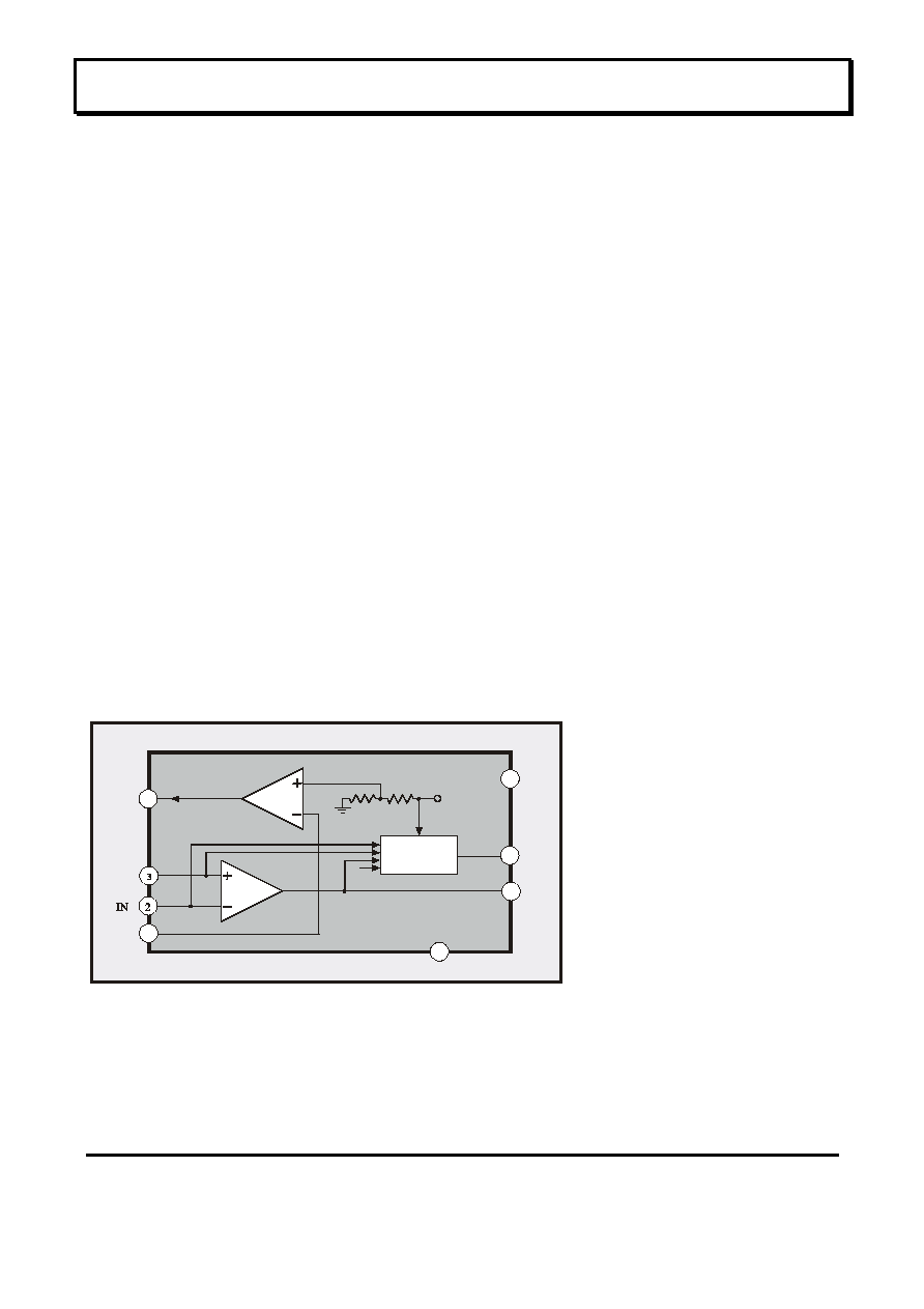
BLOCK DIAGRAM
OP
AMP
Temp
V
CC
AM457
1
Diagnostic
unit
4
5
6
7
8
OUTOP
IN+
INOP
GND
OUT
DIAG
VCC
_
1k
9k
Figure 1: Block diagram

Precision amplifier for bridge circuits
AM457
analog microelectronics
May 2005
Analog Microelectronics GmbH
Phone: +49 (0)6131/91 073 ≠ 0
4/10
An der Fahrt 13, D ≠ 55124 Mainz
Fax:
+49 (0)6131/91 073 ≠ 30
Rev. 2.2
Internet: www.analogmicro.de
Email: info@analogmicro.de
ELECTRICAL SPECIFICATIONS
T
amb
= 25∞C, V
CC
= 5V (unless otherwise stated)
Parameter
Symbol
Conditions
Min.
Typ.
Max.
Unit
Voltage Range
V
CC
4.5 5 5.5 V
Quiescent Current
I
CC
T
amb
= -40...+85∞C
1.5
2.5
mA
Temperature Specifications
Operating
T
amb
-45
125
∞C
Storage
T
st
-55
150
∞C
Junction
T
J
150
∞C
Thermal Resistance
ja
DIL8 plastic package
111
∞C/W
ja
SO8 narrow plastic package
181
∞C/W
Amplifier AMP
Offset Voltage
V
OS
±0.1
±0.3
mV
V
OS
vs. Temperature
dV
OS
/dT
T
amb
= -45...105∞C
±0.5
±1.2
µV/∞C
V
OS
vs. Temperature
dV
OS
/dT
T
amb
= 105...125∞C
±120
µV
Input Bias Current
I
B
30
200
nA
I
B
vs. Temperature
dI
B
/dT
V
CM
= 2.5V
T
amb
= -45...125∞C
≠130
≠600
pA/∞C
Differential Input Voltage
V
IN
V
IN
=V
IN+
≠ V
IN-
±5
±100
mV
Input Offset Current
I
OS
±0.5
±5
nA
I
OS
vs. Temperature
dI
OS
/dT
V
CM
= 2.5V
T
amb
= -45...125∞C
±2.5
±30
pA/∞C
Input Resistance
R
IN
V
CM
/ I
B,typ
(V
CM
= 2.5V)
100
M
Input Capacitance
C
IN
90
pF
Common Mode Input Range
CMIR
1
VCC ≠ 1.3
V
Common Mode Rejection Ratio
CMRR
120
135
dB
Open Loop Gain
G
0
120
140
dB
Adjustable Gain
G
10
Output Voltage Range
V
OUT
0.2
VCC ≠ 0.2
V
Output Current
I
OUT
Sink and source
250
µA
Output Load Capacitance
C
L
1 5 nF
Output Load Resistance
R
L
Sink and source
20
k
Power Supply Rejection Ratio
PSRR
90
110
dB
Gain Bandwidth Product
GBW
G = 10; C
1
= 1nF; R
L
= 20k
Including filters for EMC
protection
30
kHz
Non Linearity
G
100
10
-4
Slew Rate
SR
C
1
= 1nF; R
L
= 20k
0.3 0.8 V/µs
Input Voltage Noise
e
n
T
amb
, ;Rs = 1k
; V
CC
= 5V
Rs = Source Impedance
30
nV/
Hz

Precision amplifier for bridge circuits
AM457
analog microelectronics
May 2005
Analog Microelectronics GmbH
Phone: +49 (0)6131/91 073 ≠ 0
5/10
An der Fahrt 13, D ≠ 55124 Mainz
Fax:
+49 (0)6131/91 073 ≠ 30
Rev. 2.2
Internet: www.analogmicro.de
Email: info@analogmicro.de
Error Monitoring (Diagnosis)
Output Voltage on Error (high)
V
DIAG
VCC ≠ 0.2
V
Output Voltage without Error (low)
V
DIAG
GND+
0.2
V
Output Current on Error
I
ERR
V
DIAG
= 2.5V
1.5
3.5
6
µA
Output Current without Error
I
NOERR
V
DIAG
= 2.5V
-6
-3.5
-1.5
µA
Threshold for
Temperature
Error Monitor-
ing
T
ERR
105 143
∞C
Threshold for Output Current (AMP) Error
Monitoring
I
IA,ERR
250 800
µA
Threshold for Supply Voltage Error
Monitoring
V
CC,ERR
3.8 4.3 V
Threshold for High Input Voltage (AMP)
Error Monitoring
V
IN,high,ERR
With regard to the sensing element VCC ≠ 1.8
VCC ≠ 0.8
V
Threshold for Low Input Voltage (AMP)
Error Monitoring
V
IN,low,ERR
0.4 0.9 V
Operational Amplifier (OP)
Offset Voltage
V
OS
±4
±8
mV
V
OS
vs. Temperature
dV
OS
/dT
T
amb
= -45...105∞C
±10
±40
µV/∞C
V
OS
vs. Temperature
dV
OS
/dT
T
amb
= 105...125∞C
±320
µV
Input Bias Current
I
B
80 300
nA
I
B
vs. Temperature
dI
B
/dT
T
amb
= -45...125∞C
100
400
pA/∞C
Input Resistance
R
IN
V
CM
/ I
B,typ
(V
CM
= 0.5V)
6.25
M
Input Capacitance
C
IN
30
pF
Common Mode Input Range
CMIR
0
0.5
1
V
Open Loop Gain
G
0
I
0ut
=0.1mA
90
110
dB
G
0.2mA
I
0ut
=2mA
75
90
dB
Output Voltage Range
V
OUT
0
VCC ≠ 0.2
V
Output Source Current
I
OUT
PNP Open Collector Output
2
mA
Output Load Capacitance
C
1
1 5
nF
Gain Bandwidth Product
GBW
G
GAIN
= 10; C
1
= 1nF; R
L
= 1.25k
0.9 1.4 MHz
Slew Rate
SR
G
GAIN
= 100; C
1
= 1nF; R
L
= 25k
0.2 0.7 V/µs
Table 1: Specifications
Currents flowing into the IC are negative. Positive input of the o
perational amplifier (fixed internally): 0.1
V
CC
V
CM
Input Common Mode Voltage
CIRCUIT
Parameter
Symbol
Conditions
Min.
Typ.
Max.
Unit
AMP Output Capacitor
C
1
1 5 nF
Compensation Capacitor
C
2
100 pF
DIAG Output Capacitor (optional)
C
3
3.3
nF
OP Output Capacitor (optional)
C
4
1 5 nF
Stabilization Capacitor (optional)
C
5
100
nF
EMV Protection Capacitor (optional)
C
6
470
pF
Load Resistor
R
L
20
k
Table 2: Circuit Components
Recommendation: Ceramic capacitor