Analog Microelectronics, Inc.
1
AME1084
5A Low Dropout
Positive Voltage Regulator
n
n
n
n
n
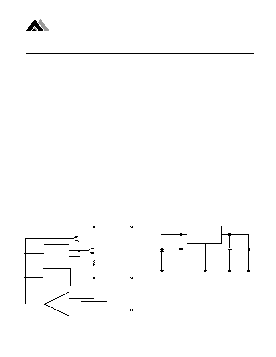
Functional Block Diagram
n
n
n
n
n
General Description
The AME1084 is a 5A low-dropout positive voltage regu-
lator. It is available in fixed and adjustable output volt-
age versions. Overcurrent and thermal protection are
integrated onto the chip. Output current will limit as it
reaches the pre-set current or temperature limit. At full
rated output current the dropout voltage is 1.4V (max.).
AME1084 series regulators provide excellent regulation
over line, load and temperature variations.
n
n
n
n
n
Key Features
l
Low dropout voltage
...
1.4V at 5A
l
l
l
l
l
Adjustable or 3.3V fixed voltage
l
l
l
l
l
Line regulation typically 0.015%
l
l
l
l
l
Load regulation typically 0.05%
l
l
l
l
l
Adjust pin (ADJ) current less than 90
�
A
l
l
l
l
l
Overcurrent protection
l
l
l
l
l
Thermal protection
l
l
l
l
l
Available in TO-220, TO-263, TO-252
n
n
n
n
n
Applications
l
l
l
l
l
High Efficiency Linear Regulators
l
l
l
l
l
Post Regulators for Switching Supplies
l
l
l
l
l
5V to 3.3V Voltage Converter
l
l
l
l
l
Battery Charger
Figure 1
T h e r m a l
Protection
B a n d g a p
R e f e r e n c e
Current
Limiting
Amplifier
Input
Output
A D J / G N D
Error
A m p .
Figure 2
n
n
n
n
n
Typical Application
AME1084
Load
10
�
F Tan
10
�
F Tan
4.75V to 5.25V
V
I N
G N D
V
O U T
Analog Microelectronics, Inc.
2
AME1084
5A Low Dropout
Positive Voltage Regulator
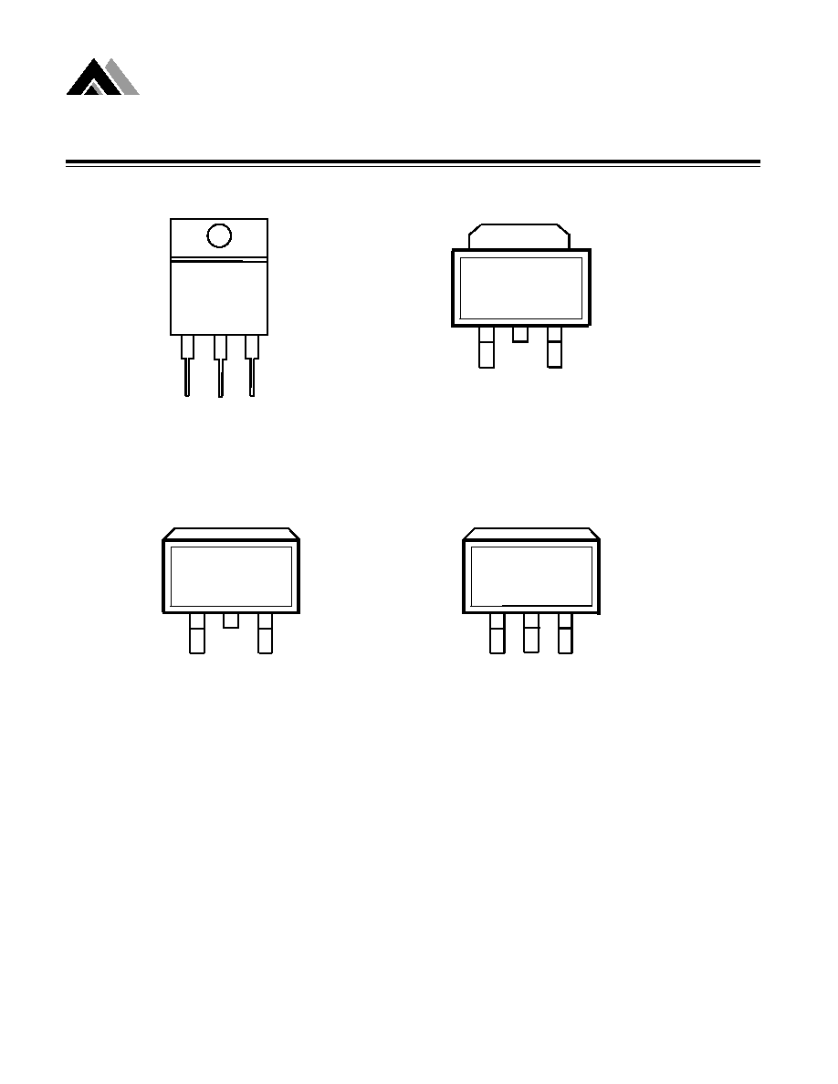
TO-220 Front View
TO-263-3 Front View
n
n
n
n
n
Pin Configuration
V
IN
A D J / G N D
V
O U T
AME1084
1
2
3
AME 1084
A D J / G N D V
O U T
V
IN
1
2
3
AME 1084
A D J / G N D V
O U T
V
IN
TO-263-2 Front View
1
2
3
AME 1084
A D J / G N D V
O U T
V
IN
To-252 Front View

Analog Microelectronics, Inc.
3
AME1084
5A Low Dropout
Positive Voltage Regulator
P a rt Num be r
M a rking
Output V olta ge
P a cka ge
A M E 1084A CB T
A M E 1084
A CB T
y y ww
A DJ
TO-220
A M E 1084B CB T
A M E 1084
B CB T
y y ww
1.5
TO-220
A M E 1084CCB T
A M E 1084
CCB T
y y ww
2.5
TO-220
A M E 1084DCB T
A M E 1084
DCB T
y y ww
3.3
TO-220
A M E 1084A CDT-3
A M E 1084
A CDT-3
y y ww
A DJ
TO-263-3
A M E 1084B CDT-3
A M E 1084
B CDT-3
y y ww
1.5
TO-263-3
A M E 1084CCDT-3
A M E 1084
CCDT-3
y y ww
2.5
TO-263-3
A M E 1084DCDT-3
A M E 1084
DCDT-3
y y ww
3.3
TO-263-3
A M E 1084A CDT
A M E 1084
A CDT
y y ww
A DJ
TO-263-2
A M E 1084B CDT
A M E 1084
B CDT
y y ww
1.5
TO-263-2
A M E 1084CCDT
A M E 1084
CCDT
y y ww
2.5
TO-263-2
A M E 1084DCDT
A M E 1084
DCDT
y y ww
3.3
TO-263-2
A M E 1084A CCS
A M E 1084
A CCS
y y ww
A DJ
TO-252
A M E 1084B CCS
A M E 1084
B CCS
y y ww
1.5
TO-252
A M E 1084CCCS
A M E 1084
CCCS
y y ww
2.5
TO-252
A M E 1084DCCS
A M E 1084
DCCS
y y ww
3.3
TO-252
n
n
n
n
n
Ordering Information

Analog Microelectronics, Inc.
4
AME1084
5A Low Dropout
Positive Voltage Regulator
n
n
n
n
n
Absolute Maximum Ratings
Symbol
Maximum
Unit
V
IN
7
V
TO-220
3
TO-252
5
TO-263
3
TO-220
50
TO-252
90
TO-263
50
Operating Junction Temperature Range
T
J
0 to 125
Storage Temperature Range
T
STG
-65 to 150
Lead Temperature (10 sec)
T
LEAD
260
Parameter
Input Voltage
o
C
Thermal Resistance (Junction to Case)
Thermal Resistance (Junction to Ambient)
JC
JA
o
C/W

Analog Microelectronics, Inc.
5
AME1084
5A Low Dropout
Positive Voltage Regulator
n
n
n
n
n
Electrical Characteristics
1. 1084AXXX
2. 1084DXXX
Parameter
Symbol
Min.
Typ.
Max.
Units
Reference voltage
V
IN
= 5V
T
J
=25
O
C
1.238
1.262
(adjustable voltage)
I
O
= 10mA
Over temp. 1.225
1.275
V
IN
= 2.75 - 7V
T
J
=25
O
C
-
0.015
0.2
I
O
= 10mA
Over temp.
-
0.035
0.2
V
IN
= 5V
T
J
=25
O
C
-
0.05
0.3
I
O
= 10mA - 5A
Over temp.
-
0.2
0.4
Dropout voltage
V
IN
= 2.75 - 7V
T
J
=25
O
C
-
1.2
1.4
V
OUT
,
V
REF
= 1%
I
O
= 10mA - 5A
Over temp.
-
1.3
-
Current limit
I
S
V
IN
= 2.75 - 7V, Over temp.
5.0
-
-
A
Temperature Coefficient
T
C
V
IN
= 2.75 - 7V, I
O
= 10mA - 5A
-
0.005
-
%/
O
C
V
IN
= 2.75 - 7V
T
J
= 25
O
C
-
55
-
I
O
= 10mA - 5A
Over temp.
-
-
90
V
IN
= 2.75 - 7V, I
O
= 10mA - 5A
Over temp.
Temperature stability
T
S
V
IN
= 5V, I
O
= 500mA, Over temp.
0.5
0.5
-
%
Minimum load current
I
O
V
IN
= 5V
-
5
10
mA
RMS output noise
V
N
T
J
= 25
O
C
-
0.003
-
%V
O
Ripple rejection ratio
R
A
V
IN
= 5V, I
O
= 5A, Over temp.
60
72
-
dB
Test Conditions
V
D
I
ADJ
I
ADJ
Line regulation
Load regulation
Reg
LINE
V
REF
Reg
LOAD
Adjust pin current
Adjust pin current change
0.2
5
-
�
A
1.250
V
V
%
%
Parameter
Symbol
Min.
Typ.
Max.
Units
Output voltage
V
IN
= 5V
T
J
=25
O
C
3.267
3.333
(fixed voltage)
I
O
= 0A
Over temp. 3.234
3.366
V
IN
= 4.5 - 7V
T
J
=25
O
C
-
0.015
0.2
I
O
= 0A
Over temp.
-
0.035
0.2
V
IN
= 5V
T
J
=25
O
C
-
0.05
0.3
I
O
= 0A - 5A
Over temp.
-
0.2
0.4
Dropout voltage
V
IN
= 4.5 - 7V
T
J
=25
O
C
-
1.2
1.4
V
OUT
,
V
REF
= 1%
I
O
= 0A - 5A
Over temp.
-
1.3
-
Current limit
I
S
V
IN
= 4.5 - 7V, Over temp.
5.0
-
-
A
Quiescent current
(fixed model)
Temperature Coefficient
T
C
V
IN
= 4.5 - 7V, I
O
= 0A - 5A
-
0.005
-
%/
0
C
Temperature stability
T
S
V
IN
= 5V, I
O
= 500mA, Over temp.
0.5
0.5
-
%
RMS output noise
V
N
-
0.003
-
%V
O
Ripple rejection ratio
R
A
V
IN
= 5V, I
O
= 5A, Over temp.
60
72
-
dB
Line regulation
Reg
LINE
%
Test Conditions
Vo
3.300
Load regulation
Reg
LOAD
%
V
D
V
T
J
= 25
O
C
I
Q
V
IN
=5V, Io=0-5A, Over temp.
-
13
mA
12
V