Analog Microelectronics, Inc.
1
AME1085
3A Low Dropout
Positive Voltage Regulator
n
n
n
n
n
Applications
l
l
l
l
l
High Efficiency Linear Regulators
l
l
l
l
l
Post Regulators for Switching Supplies
l
l
l
l
l
5V to 3.3V Voltage Converter
l
l
l
l
l
Battery Charger
n
n
n
n
n
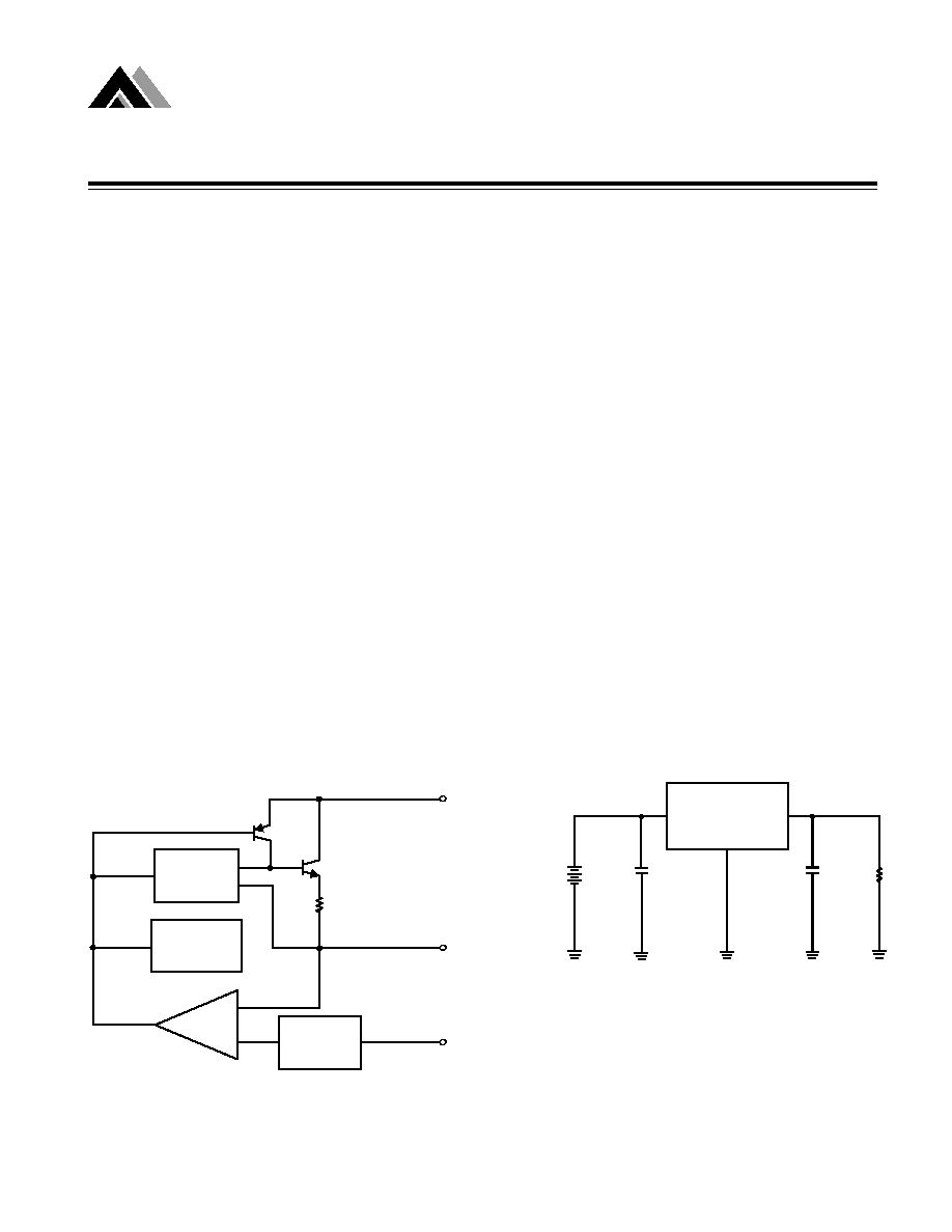
Functional Block Diagram
Thermal
Protection
B a n d g a p
Reference
Current
Limiting
Amplifier
Input
Output
A D J / G N D
Error
A m p .
n
n
n
n
n
General Description
The AME1085 is a 3A low-dropout positive voltage regu-
lator. It is available in fixed and adjustable output voltage
versions. Overcurrent and thermal protection are inte-
grated onto the chip. Output current will limit as it reaches
the pre-set current or temperature limit. At full rated
output current the dropout voltage is 1.4V (max.).
AME1085 series regulators provide excellent regulation
over line, load and temperature variations.
n
n
n
n
n
Key Features
l
Low dropout voltage
1.2V typically at 3A
l
l
l
l
l
Adjustable or 3.3V fixed voltage
l
l
l
l
l
Line regulation typically 0.015%
l
l
l
l
l
Load regulation typically 0.05%
l
l
l
l
l
Adjust pin (ADJ) current less than 90
A
l
l
l
l
l
Overcurrent protection
l
l
l
l
l
Thermal protection
l
l
l
l
l
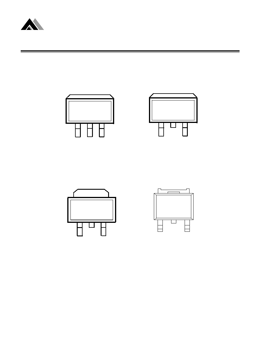
Available in TO-220, TO-263, TO-252
Figure 1
n
n
n
n
n
Typical Application
Figure 2
AME1085
L o a d
10
µ
F Tan
10
µ
F Tan
4.75V to 5.25V
V
I N
G N D
V
O U T

Analog Microelectronics, Inc.
3
AME1085
3A Low Dropout
Positive Voltage Regulator
n
n
n
n
n
Absolute Maximum Ratings
n
n
n
n
n
Ordering Information
Symbol
Maximum
Units
V
IN
7
V
TO-220
2.5
TO-263
2.5
TO-252
15
TO-220
50
TO-263
60
TO-252
90
Thermal Resistance
(Junction to Case)
Storage Temperature Range
Operating Junction Temperature Range
Parameter
0
C
JC
0
C/W
T
LEAD
260
JA
Thermal Resistance
(Junction to Ambient)
Lead Temperature ( 10 sec )
Input Voltage
T
J
0 to 125
T
STG
-65 to 150
Part Number
Marking
Output Voltage
Package
AME1085ACBT
AME1085
ACBT
YYWW
ADJ
TO-220
AME1085DCBT
AME1085
DCBT
YYWW
3.3
TO-220
AME1085ACDT-3
AME1085
ACDT-3
YYWW
ADJ
TO-263-3
AME1085DCDT-3
AME1085
DCDT-3
YYWW
3.3
TO-263-3
AME1085ACDT
AME1085
ACDT
YYWW
ADJ
TO-263-2
AME1085DCDT
AME1085
DCDT
YYWW
3.3
TO-263-2
AME1085AMCT
AME1085
AMCT
YYWW
ADJ
TO-252-2
AME1085MCT*
AME1085
MCT
YYWW
3.3
TO-252-2
* This differs from our standard part numbering scheme due to historical precedent
Analog Microelectronics, Inc.
4
AME1085
3A Low Dropout
Positive Voltage Regulator
n
n
n
n
n
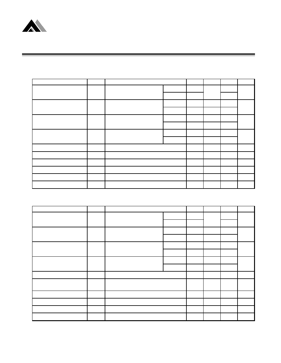
Electrical Characteristics
AME1085DXXX
AME1085AXXX
Parameter
Symbol
Min.
Typ.
Max.
Units
Reference voltage
V
IN
= 5V
T
J
=25
0
C
1.238
1.262
(adjustable voltage)
I
O
= 10mA
Over temp.
1.225
1.275
V
IN
= 2.75 - 7V
T
J
=25
0
C
-
0.015
0.2
I
O
= 10mA
Over temp.
-
0.035
0.2
V
IN
= 5V
T
J
=25
0
C
-
0.05
0.3
I
O
= 10mA - 3A
Over temp.
-
0.2
0.4
Dropout voltage
V
IN
= 2.75 - 7V
T
J
=25
0
C
-
1.2
1.4
V
OUT
,
V
REF
= 1%
I
O
= 10mA - 3A
Over temp.
-
1.3
-
Current limit
I
S
3.0
-
-
A
Temperature Coefficient
T
C
-
0.005
-
%/
O
C
Temperature stability
T
S
V
IN
= 5V, I
O
= 500mA, Over temp.
-
0.5
-
%
Minimum load current
I
O
-
5
10
mA
RMS output noise
V
N
-
0.003
-
%V
0
Ripple rejection ratio
R
A
V
IN
= 5V, I
O
= 3A, Over temp.
60
72
-
dB
Test Conditions
V
REF
1.250
V
Line regulation
Reg
LINE
%
Load regulation
Reg
LOAD
%
V
D
V
V
IN
= 2.75 - 7V, Over temp.
V
IN
= 2.75 - 7V, I
O
= 10mA - 3A
V
IN
= 5V
T
J
=25
0
C
Parameter
Symbol
Min.
Typ.
Max.
Units
Output voltage
V
IN
= 5V
T
J
=25
0
C
3.267
3.333
(fixed voltage)
I
O
= 0A
Over temp.
3.234
3.366
V
IN
=4.5 - 7V
T
J
=25
0
C
-
0.015
0.2
I
O
= 0A
Over temp.
-
0.035
0.2
V
IN
= 5V
T
J
=25
0
C
-
0.05
0.3
I
O
= 0A - 3A
Over temp.
-
0.2
0.4
Dropout voltage
V
IN
= 4.5 - 7V
T
J
=25
0
C
-
1.2
1.4
V
OUT
,
V
REF
= 1%
I
O
= 0A - 3A
Over temp.
-
1.3
-
Current limit
I
S
3.0
-
-
A
Quiescent current
(fixed model)
Temperature Coefficient
T
C
-
0.005
-
%/
0
C
Temperature stability
T
S
V
IN
= 5V, I
O
= 500mA, Over temp.
-
0.5
-
%
RMS output noise
V
N
-
0.003
-
%V
0
Ripple rejection ratio
R
A
V
IN
= 5V, I
O
= 3A, Over temp.
60
72
-
dB
Test Conditions
Vo
3.300
V
Line regulation
Reg
LINE
%
Load regulation
Reg
LOAD
%
V
D
V
V
IN
= 4.5 - 7V, Over temp.
I
Q
V
IN
= 5V, Io=0A - 3A, Over temp.
-
T
J
=25
0
C
12
13
mA
V
IN
= 4.5 - 7V, I
O
= 0A - 3A

Analog Microelectronics, Inc.
5
AME1085
3A Low Dropout
Positive Voltage Regulator
n
n
n
n
n
Application Description
1. Output voltage adjustment
Like most regulators, the AME1085 regulates the
output by comparing the output voltage to an
internally generated reference voltage. On the
adjustable version, the V
REF
is available exter-
nally as 1.25V between V
OUT
and ADJ. The
voltage ratio formed by R1 and R2 should be
set
to conduct 10mA (minimum output load).
The output voltage is given by the following
equation:
V
OUT
= V
REF
( 1 + ) + I
ADJ
x R2
On fixed versions of AME1085, the voltage di-
vider is provided internally.
R2
R1
Figure 3
2. Thermal protection
AME1085 has thermal protection which limits
junction temperature to 150
O
C. However, de-
vice
functionality is only guaranteed to a maxi-
mum junction temperature of +125
O
C.
The power dissipation and junction temperature
for AME1085 in TO-220 package are given by
P
D
= (V
IN
- V
OUT
) x I
OUT
T
JUNCTION
= T
AMBIENT
+ ( P
D
x
JA
)
Note: T
JUNCTION
must not exceed 125
O
C
3. Current limit protection
AME1085 is protected against overload condi-
tions. Current protection is triggered at typi-
cally 4.5A.
4. Stability and load regulation
AME1085 requires a capacitor from V
OUT
to
GND to provide compensation feedback to the
internal gain stage. This is to ensure stability
at the output terminal. Typically, a 10
µ
F tanta-
lum or 50
µ
F aluminum electrolytic is sufficient.
Note: It is important that the ESR for this ca-
pacitor does not exceed 0.5
.
The output capacitor dose not have a theoreti-
cal upper limit and increasing its value will in-
crease stability. C
OUT
= 100
µ
F or more is typi-
cal for high current regulator design.
For the adjustable version, the best load regu-
lation is accomplished when the top of the
resistor divider (R1) is connected directly to the
output pin of the AME1085. When so con-
nected, R
P
is not multiplied by the divider ratio.
For fixed output versions, the top of R1 is in-
ternally connected to the output and ground
pin can be connected to low side of the load.
Figure 4
V
O U T
= V
R E F
(1+ R 2
R 1
) + I
A D J
x R2
O U T
A D J
IN
V
R E F
I
A D J
50
µ
A
V
IN
V
O U T
R 1
R 2
C
1
O U T
A D J
IN
V
IN
R 1
R 2
R
L
R
P
Parasitic
Line Resistance
Connect
R2 to load
(Connect R1 to case)