Analog Microelectronics, Inc.
1
AME385-2.5
Micropower Voltage Reference Diode
n
n
n
n
n
General Description
The AME385-2.5 is a micropower 2-terminal band-gap
voltage regulator diode. It operates over a 20
µ
A to 20mA
current range. Each circuit is trimmed at wafer sort to
provide a
±
0.20% and
±
0.50% initial tolerance. The de-
sign of the AME385-2.5 allows for a large range of load
capacitances and operating currents. The low start-up
current makes these part ideal for battery applications.
Analog Microelectronics offers this part in a TO-92 and
SO-8 package as well as the space saving SOT-23.
n
n
n
n
n
Key Features
l
Small packages: SOT-23, TO-92, SO-8
l
Tolerates capacitive loads
l
Fixed reverse breakdown voltage of 2.5V
l
Tight voltage tolerance ----------
±
0.20%,
±
0.50%
l
Wide operating current ---------- 20
µ
A to 20mA
l
Wide temperature range -------- -40
o
C to +85
o
C
l
Low temperature coefficient --- 100ppm/
o
C (max)
l
Excellent transient response
n
n
n
n
n
Typical Application
n
n
n
n
n
Applications
l
Portable electronics
l
Power supplies
l
Computer peripherals
l
Data acquisition systems
l
Battery chargers
l
Consumer electronics
n
n
n
n
n
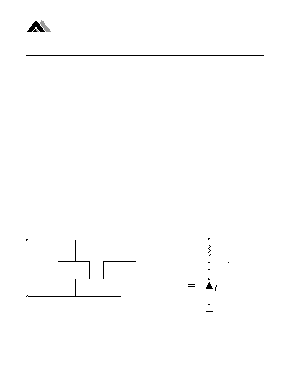
Functional Block Diagram
G ND
V R
B andgap
Cell
Current
S hunt
V S
V R
RS =
V S - V R
I
V R = 2.5V
1000pF
V alue optional
RS
I

Analog Microelectronics, Inc.
2
Micropower Voltage Reference Diode
AME385-2.5
n
n
n
n
n
Ordering Information
n
n
n
n
n
Package Outline
* The NC pin must float or be connected to - (negative)
+
-
+
-
N C
*
N C
*
+
-
SOT-23 Top View
TO-92-3 Bottom View
TO-92-2 Bottom View
N C
+
-
N C
N C
N C
N C
N C
1
2
3
4
5
6
7
8
SO-8 Top View
P a rt N u m b e r
Ac c u ra c y
M a rk in g
P a c k a g e
O p e ra tin g T e m p . R a n g e
A M E 3 8 5 D E E T
0 .2 %
A C S ww
S O T-2 3
-4 0
O
C to +8 5
O
C
A M E 3 8 5 D E HA
0 .2 %
A M E
3 8 5 D E HA
yyww
S O -8
-4 0
O
C to +8 5
O
C
A M E 3 8 5 B E E T
0 .5 %
A B Yww
S O T-2 3
-4 0
O
C to +8 5
O
C
A M E 3 8 5 B E A T
0 .5 %
A M E
3 8 5
B E A T
yyww
TO -9 2 -3
-4 0
O
C to +8 5
O
C
A M E 3 8 5 B E A S
0 .5 %
A M E
3 8 5
B E A S
yyww
TO -9 2 -2
-4 0
O
C to +8 5
O
C
A M E 3 8 5 B E HA
0 .5 %
A M E
3 8 5 B E HA
yyww
S O -8
-4 0
O
C to +8 5
O
C
P leas e c ons ult AME s ales offic e or authoriz ed R ep./D is tributor for other voltage ac c urac y and
pac kage type availability.
Analog Microelectronics, Inc.
3
AME385-2.5
Micropower Voltage Reference Diode
n
n
n
n
n
Absolute Maximum Ratings
n
n
n
n
n
Recommended Operating Conditions
n
n
n
n
n
Thermal Information
Caution: Stress above the listed absolute rating may cause permanent damage to the device
P a ra m e te r
Ra ting
Unit
S upply Current
100
µ
A ~ 20m A
A m bient Tem perature Range
-40 to + 85
o
C
Junc tion Tem perature
-40 to + 125
o
C
P a ra m e te r
M a x im u m
Un it
S upply Current
50
m A
M a x im u m
U n it
S O T-23
325
TO -92
180
S O -8
125
M ax im um Junc tion Tem perature
150
o
C
M ax im um Lead Tem perature ( 10 S ec )
300
o
C
P a ra m e te r
o
C / W
Therm al R es is tanc e
Analog Microelectronics, Inc.
4
Micropower Voltage Reference Diode
AME385-2.5
n
n
n
n
Electrical Specifications
Unless otherwise specified, TA
=
0~70
o
C, I
=
100
µ
A
PARAMETER
SYMBOL
TEST CONDITIONS
MIN
TYP
MAX
UNITS
Reference Voltage,
±
0.2%
2.495
2.50
2.505
V
Reference Voltage,
±
0.5%
2.487
2.50
2.513
V
Minimum Current
I
MIN
20
µ
A
I
MIN
< I < 1mA
1.5
3
1mA < I < 20mA
5
20
Maximum Operation Current
ILmax
20
mA
Reverse Dynamic Impedence
RDI
IR= 100mA, f=20Hz
1.5
Ohm
Wideband Noise (rms)
Vn
IR= 100mA, 10 Hz<f<10KHz
60
µ
V
Long term Stability
IR= 100mA, TA=25
o
C,
T=1000 Hours
20
ppm
Reference Voltage Temp. Coeff.
V
REFTC
0
o
C < T
A
< 70
o
C
100
ppm/
o
C
Reference Voltage Change With
Current
dV
REF/I
mV
I
REF
=
100
µ
A
V
REF
Analog Microelectronics, Inc.
5
AME385-2.5
Micropower Voltage Reference Diode
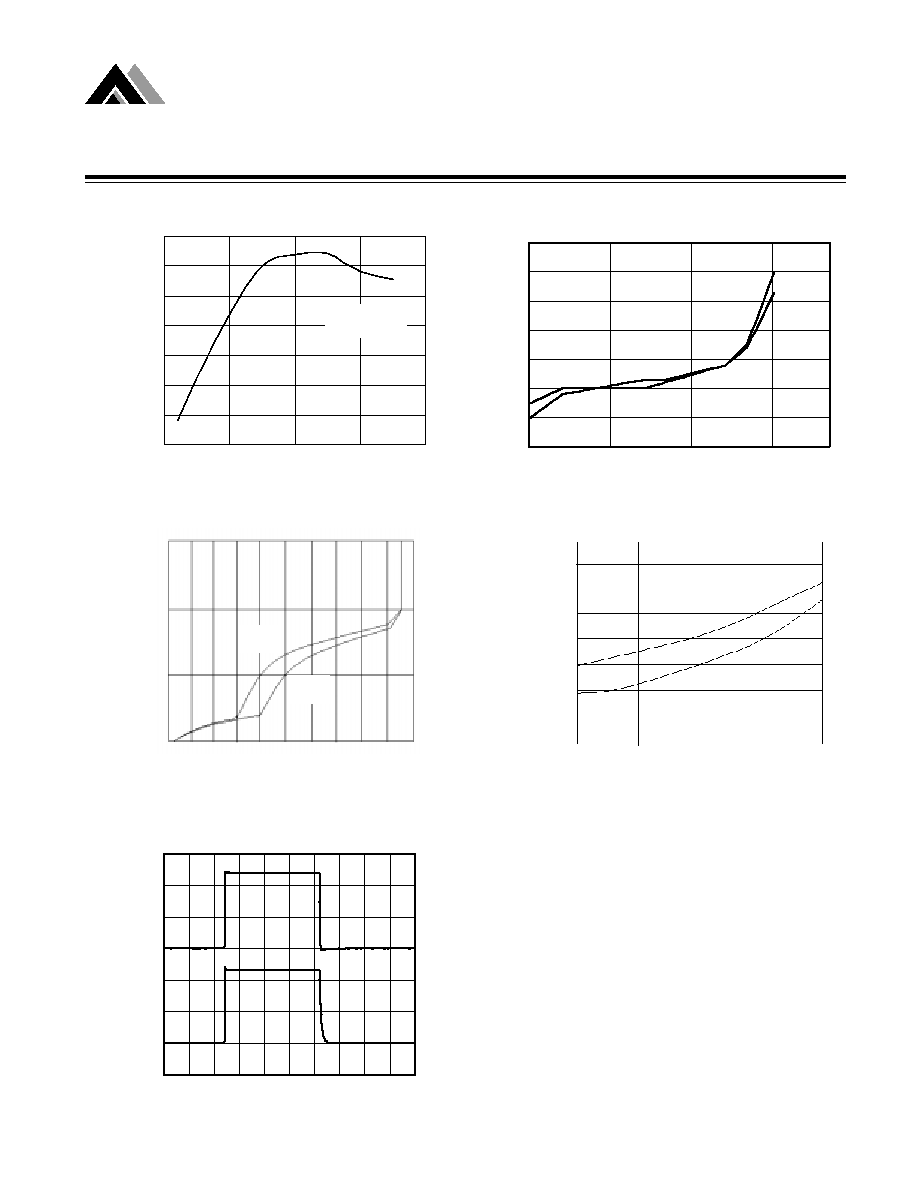
Output Voltage Change vs. Current
Reverse Characteristic
25
o
C
85
o
C
0.0V
0.65V
1.3V
V
R
100
µ
A
10
µ
A
1
µ
A
100nA
I
R
-0.6
-0.5
-0.4
-0.3
-0.2
-0.1
0
0.1
-50
0
50
100
150
Normalized Percentage Change vs.
Temperature
% Change of V
OUT
(
O
C)
I = 100
µ
A
0.0V
1.0V
0.125V/DIV
85
o
C
25
o
C
Forward Characteristic
1
µ
A
100
µ
A
10mA
Transient Response
200
µ
S/DIV
V R
V
IN
5 V / D I V
1 V / D I V
2 5
oC
(m A )
(mV)
0 .0
1
1 0 0
-2
0
2
4