
AME, Inc.
1
AME5130
Micropower Step-Up DC/DC Converter
The AME5130 is a fixed off-time step-up DC/DC con-
verter in a small 5-lead SOT-25 package.The AME5130
is ideal for LCD panels requiring low current and high effi-
ciency as well as LED applications for cellular phone back-
lighting, PDAS,and other hand-held devices. The low
400ns off-time allows the use of tiny external compo-
nents.
AME5130 can drive up 8 white LEDs from a single Li-
Ion battery DC 2V to 5.5V; can be turned on by putting
more than 1V at pin 4(RUN). To control LED brightness,
the LED current can be pulsed by applying a PWM (pulse
width modulated) signal with a frequency range of 100Hz
to 50KHz to the RUN pin.
n
General Description
n
Features
n
Applications
n
Typical Application
l
0.7
internal switch
l
Uses small surface mount components
l
Adjustable output voltage up to 20V
l
2V to 5.5V input range
l
Input undervoltage lockout
l
0.01
�
A shutdown current
l
Small 5-Lead SOT-25 package
l
White LED Back-Lighting
l
Hand-held Devices
l
Digital Cameras
l
Portable Applications
l
LCD Bias Power
Figure 1
Six White LEDs Application in Li-lon
Battery
Figure 2
Typical 20V Application
C
IN
4.7
�
F
Ceramic
2
5
1
L
15
�
H
4
V
IN
2.5V-4.2V
3
R2
33K
D
AME5130
SW
V
IN
FB
GND
RUN
C
OUT
4.7
�
F
Ceramic
R1
510K
20V
20mA
C
IN
4.7
�
F
Ceramic
AME5130
V
IN
SW
FB
RUN
GND
2
5
1
L
10
�
H
4
0V
>1.1V
V
IN
2.5V-4.2V
3
R2
80
C
OUT
4.7
�
F
Ceramic
D
Option for
6LEDs
I
LED
* I
LED
=V
FB
/R2

AME, Inc.
2
Micropower Step-Up DC/DC Converter
AME5130
Figure 3
AME5130 Block Diagram
n
Function Block Diagram
C
IN
Driver
Enable
Comp
-
SW
V
IN
L
D
RUN
GND
FB
R1
R2
V
OUT
V
OUT
V
IN
400ns one
Shot
Internal
Soft Start
+
Logic
control
Current sensing
Vref=1.23
CL
Comp
+
-
C
OUT
Under Voltage
Lockout

AME, Inc.
3
AME5130
Micropower Step-Up DC/DC Converter
AME5130
1. SW
2. GND
3. FB
4. RUN
5. V
IN
* Epoxy: Conductive
SOT-25
Top View
1
3
2
5
4
AME5130
n
Pin Configuration
n
Pin Description
Pin #
Pin Name
Pin Description
1
SW
Power Switch input.
This is the drain of the internal NMOS power switch. Minimize the metal trace area
connected to this pin to minimize EMI.
2
GND
Ground.
Tie directly to ground plane.
3
FB
Output voltage feedback input.
Set the output voltage by selecting values for R1 and R2 using:
Connect the ground of the feedback network to an AGND(Analog Ground) plane which
should be tied directly to the GND pin.
4
RUN
Shutdown control input, active low.
The shutdown pin is an active low control. Tie this pin above 1V to enable the device.
Tie this pin below 0.4V to turn off the device.
5
V
IN
Analog and Power input.
Input Supply Pin. Bypass this pin with a capacitor as close to the device as possible.
-
=
1
23
.
1
2
1
V
V
R
R
out
AME, Inc.
4
Micropower Step-Up DC/DC Converter
AME5130
n
Ordering Information
Note: ww represents the date code and pls refer to Date Code Rule before Package Dimension.
* A line on top of the first letter represents lead free plating such as BCL.
Please consult AME sales office or authorized Rep./Distributor for the availability of package type.
Operating Temperature Range
Number of Pins
Package Type
Pin Configuration
Special Feature
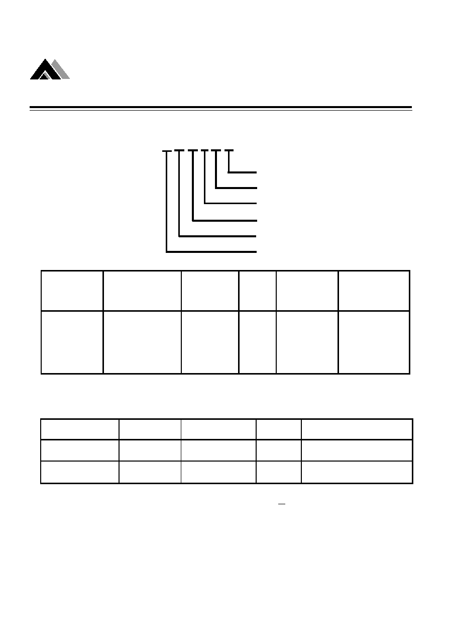
AME5130 x x x
x
x
x
Output Voltage
n
Ordering Information
A
1. SW
E: -40
O
C to 85
O
C
E: SOT-2X
V: 5
ADJ: Adjustable
Z: Lead free
2. GND
3. FB
4. RUN
5. V
IN
Output Voltage
Special Feature
Pin
Configuration
Operating
Temperature Range
Package Type
Number
of
Pins
Part Number
Marking*
Output Voltage Package Operating Temp. Range
AME5130AEEVADJ
BCLww
ADJ
SOT-25
-40
O
C to +85
O
C
AME5130AEEVADJZ
BCLww
ADJ
SOT-25
-40
O
C to +85
O
C

AME, Inc.
5
AME5130
Micropower Step-Up DC/DC Converter
Parameter
Package
Die Attached Symbol
Maximum
Unit
Thermal Resistance*
(Junction to Case)
J
C
81
Thermal Resistance
(Junction to Ambient)
JA
260
Internal Power Dissipation
(
T = 100
o
C)
P
D
400
mW
150
o
C
300
o
C
o
C / W
Maximum Junction Temperature
Lead Temperature (Soldering 10sec)
SOT-25
Conductive
n
Absolute Maximum Ratings
n
Recommended Operating Conditions
Caution: Stress above the listed absolute maximum rating may cause permanent damage to the device
n
Thermal Information
* The case point of
JC
is on the center of Molding Compound.
Parameter
Rating
Unit
Ambient Temperature Range
-40 to +85
o
C
Junction Temperature
-40 to +125
o
C
Parameter
Symbol
Maximum
Unit
Input Supply Voltage
V
IN
6
V
RUN, V
FB
Voltages
V
RUN
,V
FB
V
IN
V
SW Voltage
V
SW
V
OUT
+0.3
V
N-Channel Switch Sink Current
I
SW
800
mA
ESD Classification
B