
Intel and Pentium are registered trademarks of Intel Corporation. I
2
C is a licensed trademark of Philips Electronics, N.V. American Microsystems, Inc. reserves the right to change the detail specifica-
tions as may be required to permit improvements in the design of its products.
3.4.02
FS6050/FS6051/FS6053/FS6054
FS6050/FS6051/FS6053/FS6054
FS6050/FS6051/FS6053/FS6054
FS6050/FS6051/FS6053/FS6054
Low-Skew Clock Fanout Buffer ICs
Low-Skew Clock Fanout Buffer ICs
Low-Skew Clock Fanout Buffer ICs
Low-Skew Clock Fanout Buffer ICs
ISO9001
ISO9001
ISO9001
ISO9001
1.0 Features
�
Generates up to eighteen low-skew, non-inverting
clocks from one clock input
�
Supports up to four SDRAM DIMMs
�
Uses either I
2
C
�
-bus or SMBus serial interface with
Read and Write capability for individual clock output
control
�
Output enable pin tristates all clock outputs to facili-
tate board testing
�
Clock outputs skew-matched to less than 250ps
�
Less than 5ns propagation delay
�
Output impedance: 17
at 0.5V
DD
�
Serial interface I/O meet I
2
C specifications; all other
I/O are LVTTL/LVCMOS-compatible
�
Five differerent pin configurations available:
�
FS6050: 18 clock outputs in a 48-pin SSOP
�
FS6051: 10 clock outputs in a 28-pin SOIC, SSOP
�
FS6053: 13 clock outputs in a 28-pin SOIC
�
FS6054: 14 clock outputs in a 28-pin SOIC
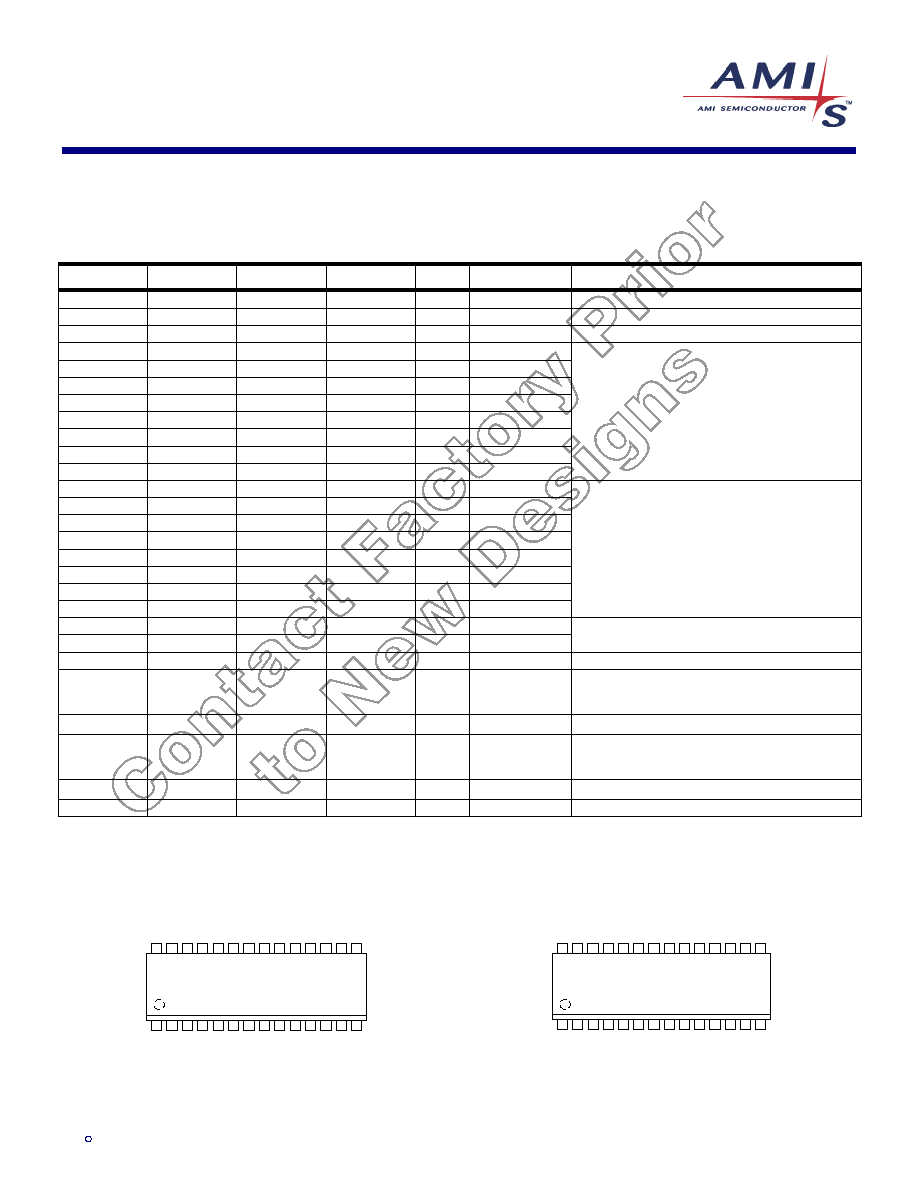
Figure 1: Block Diagram (FS6050)
Serial
Interface
SDRAM_(0:1)
SCL
SDA
CLK_IN
OE
FS6050
SDRAM_(2:3)
SDRAM_(4:5)
SDRAM_(6:7)
SDRAM_(8:9)
SDRAM_(10:11)
SDRAM_(12:13)
SDRAM_(14:15)
SDRAM_16
VSS_I
2
C
VDD_I
2
C
VSS
VDD
VSS
VDD
VSS
VDD
VSS
VDD
VSS
VDD
VSS
VDD
VSS
VDD
VSS
VDD
VSS
VDD
SDRAM_17
VSS
VDD
18
2.0 Description
The FS6050 family of CMOS clock fanout buffer ICs are
designed for high-speed motherboard applications, such
as Intel Pentium
�
II PC100-based systems with 100MHz
SDRAM.
Up to eighteen buffered, non-inverting clock outputs are
fanned-out from one clock input. Individual clocks are
skew matched to less than 250ps at 100MHz. Multiple
power and ground supplies reduce the effects of supply
noise on device performance.
Under I
2
C-bus control, individual clock outputs may be
turned on or off. An active-low output enable is available
to force all the clock outputs to a tristate level for system
testing.
Figure 2: Pin Configuration (FS6050)
1
48
2
3
4
5
6
7
8
47
46
45
44
43
42
41
(
r
es
er
v
ed)
(
r
es
er
v
ed)
VD
D
S
DRA
M_
0
S
DRA
M_
1
VSS
VD
D
S
DRA
M_
2
VS
S
SD
R
A
M
_14
SD
R
A
M
_15
(
r
es
er
v
e
d)
VD
D
(
r
es
er
v
e
d)
9
10
11
12
13
14
15
16
S
DRA
M_
3
VSS
CL
K
_
I
N
VD
D
S
DRA
M_
4
S
DRA
M_
5
VSS
VD
D
17
18
19
20
21
22
23
S
DRA
M_
6
S
DRA
M_
7
VSS
VD
D
S
DRA
M_
1
6
VSS
V
DD_
I
2
C
40
39
38
37
36
35
34
33
SD
R
A
M
_10
SD
R
A
M
_11
VD
D
OE
SD
R
A
M
_13
SD
R
A
M
_12
VS
S
VD
D
32
31
30
29
28
27
26
VS
S_I
2
C
VS
S
SD
R
A
M
_17
VD
D
SD
R
A
M
_
9
SD
R
A
M
_
8
VS
S
24
SD
A
25
SC
L
VD
D
VS
S
FS6050
48-pin SSOP
Figure 3: Pin Configuration (FS6051)
1
2
3
4
5
6
7
8
VD
D
SD
R
A
M
_
0
SD
R
A
M
_
1
VSS
VD
D
SD
R
A
M
_
2
VS
S
S
DRA
M
_
1
4
S
DRA
M
_
1
5
VD
D
9
10
11
12
13
14
15
16
SD
R
A
M
_
3
VSS
CL
K
_
I
N
VD
D
17
18
19
20
21
22
23
S
DRA
M_
1
6
VSS
V
DD_
I
2
C
VD
D
OE
S
DRA
M
_
1
3
S
DRA
M
_
1
2
VS
S
VD
D
28
27
26
V
SS_I
2
C
VS
S
S
DRA
M
_
1
7
24
SD
A
25
SC
L
FS6051
28-pin SOIC, SSOP
Additional pin configurations are noted on Page 2.
3.4.02
2
FS6050/FS6051/FS6053/FS6054
FS6050/FS6051/FS6053/FS6054
FS6050/FS6051/FS6053/FS6054
FS6050/FS6051/FS6053/FS6054
Low-Skew Clock Fanout Buffer ICs
Low-Skew Clock Fanout Buffer ICs
Low-Skew Clock Fanout Buffer ICs
Low-Skew Clock Fanout Buffer ICs
ISO9001
ISO9001
ISO9001
ISO9001
Table 1: Pin Descriptions
Key: AI = Analog Input; AO = Analog Output; DI = Digital Input; DI
U
= Input with Internal Pull-Up; DI
D
= Input with Internal Pull-Down; DIO = Digital Input/Output; DI-3 = Three-Level Digital Input,
DO = Digital Output; P = Power/Ground; # = Active Low pin
PIN (FS6050)
PIN (FS6051)
PIN (FS6053)
PIN (FS6054)
TYPE
NAME
DESCRIPTION
11
9
9
9
DI
CLK_IN
Clock input for SDRAM clock outputs
25
15
15
15
DI
U
SCL
Serial clock input
24
14
14
14
DI
U
O
SDA
Serial data input/output
4
2
2
2
DO
SDRAM_0
5
3
3
3
DO
SDRAM_1
8
6
6
6
DO
SDRAM_2
9
7
7
7
DO
SDRAM_3
13
-
-
-
DO
SDRAM_4
14
-
-
-
DO
SDRAM_5
17
-
10
10
DO
SDRAM_6
18
-
11
11
DO
SDRAM_7
SDRAM clock outputs (Byte 0)
31
-
18
18
DO
SDRAM_8
32
-
19
19
DO
SDRAM_9
35
-
-
-
DO
SDRAM_10
36
-
-
-
DO
SDRAM_11
40
22
22
22
DO
SDRAM_12
41
23
23
23
DO
SDRAM_13
44
26
26
26
DO
SDRAM_14
45
27
27
27
DO
SDRAM_15
SDRAM clock outputs (Byte 1)
21
11
12
12
DO
SDRAM_16
28
18
-
17
DO
SDRAM_17
SDRAM feedback clock outputs (Byte 2)
38
20
-
20
DI
U
OE
Output enable tristates all clock outputs when low
3, 7, 12, 16,
20, 29, 33, 37,
42, 46
1, 5, 10, 19,
24, 28
1, 5, 20, 24,
28
1, 5, 24, 28
P
VDD
3.3V � 5% power supply for SDRAM clock buffers
23
13
13
13
P
VDD_I
2
C
3.3V � 5% power supply for serial communications
6, 10, 15, 19,
22, 27, 30, 34,
39, 43
4, 8, 12, 17,
21, 25
4, 8, 17, 21,
25
4, 8, 21, 25
P
VSS
Ground for SDRAM clock buffers
26
16
16
16
P
VSS_I
2
C
Ground for serial communications
1, 2, 47, 48
-
-
-
-
(reserved)
Reserved
Figure 4: Pin Configuration (FS6053)
1
2
3
4
5
6
7
8
VD
D
SD
RAM
_
0
SD
RAM
_
1
VSS
VD
D
SD
RAM
_
2
VSS
S
DRA
M
_
1
4
S
DRA
M
_
1
5
VD
D
9
10
11
12
13
14
15
16
SD
RAM
_
3
VSS
CL
K_
I
N
SD
RAM
_
6
17
18
19
20
21
22
23
SD
RAM
_
7
S
D
R
A
M_16
V
DD_
I
2
C
S
DRA
M
_
9
VD
D
S
DRA
M
_
1
3
S
DRA
M
_
1
2
VSS
VD
D
28
27
26
VSS_
I
2
C
VSS
S
DRA
M
_
8
24
SD
A
25
SC
L
FS6053
Figure 5: Pin Configuration (FS6054)
1
2
3
4
5
6
7
8
VD
D
S
DRA
M
_
0
S
DRA
M
_
1
VS
S
VD
D
S
DRA
M
_
2
VSS
SD
RAM
_
1
4
SD
RAM
_
1
5
VD
D
9
10
11
12
13
14
15
16
S
DRA
M
_
3
VS
S
CL
K
_
I
N
S
DRA
M
_
6
17
18
19
20
21
22
23
S
DRA
M
_
7
S
DRA
M
_
1
6
VD
D_
I
2
C
SD
RAM
_
9
OE
SD
RAM
_
1
3
SD
RAM
_
1
2
VSS
VD
D
28
27
26
VSS_
I
2
C
SD
RAM
_
1
7
SD
RAM
_
8
24
SD
A
25
SC
L
FS6054

3.4.02
3
FS6050/FS6051/FS6053/FS6054
FS6050/FS6051/FS6053/FS6054
FS6050/FS6051/FS6053/FS6054
FS6050/FS6051/FS6053/FS6054
Low-Skew Clock Fanout Buffer ICs
Low-Skew Clock Fanout Buffer ICs
Low-Skew Clock Fanout Buffer ICs
Low-Skew Clock Fanout Buffer ICs
ISO9001
ISO9001
ISO9001
ISO9001
3.0 Programming
Information
Table 2: Clock Enable
CONTROL INPUTS
CLOCK OUTPUTS (MHz)
OE
SDRAM_0:17
0
tristate
1
CLK_IN
3.1 Power-Up
Initialization
All outputs are enabled and active upon power-up, and all
output control register bits are initialized to one.
The outputs must be configured at power-up and are not
expected to be configured during normal operation. Inac-
tive outputs are held low and are disabled from switching.
3.1.1 Unused
Outputs
Outputs that are not used in versions of this device with a
reduced pinout are still operational internally. To reduce
power dissipation and crosstalk effects from the unloaded
outputs, it is recommended that these outputs be shut off
via the Control Registers.
3.2 Register
Programming
A logic-one written to a valid bit location turns on the as-
signed output clock. Likewise, a logic-zero written to a
valid bit location turns off the assigned output clock.
Any unused or reserved register bits should be cleared to
zero.
Serial bits are written to this device in the order shown in
Table 3.
Table 3: Register Summary
SERIAL BIT
DATA BYTE
CLOCK OUTPUT
0
(MSB)
SDRAM_7
1
SDRAM_6
2
SDRAM_5
3
SDRAM_4
4
SDRAM_3
5
SDRAM_2
6
Byte 0
SDRAM Control Register 0
SDRAM_1
7
(LSB)
SDRAM_0
8
(MSB)
SDRAM_15
9
SDRAM_14
10
SDRAM_13
11
SDRAM_12
12
SDRAM_11
13
SDRAM_10
14
Byte 1
SDRAM Control Register 1
SDRAM_9
15
(LSB)
SDRAM_8
16
(MSB)
SDRAM_17
17
SDRAM_16
18
Reserved
19
Reserved
20
Reserved
21
Reserved
22
Byte 2
SDRAM Control Register 2
Reserved
23
(LSB)
Reserved
3.4.02
4
FS6050/FS6051/FS6053/FS6054
FS6050/FS6051/FS6053/FS6054
FS6050/FS6051/FS6053/FS6054
FS6050/FS6051/FS6053/FS6054
Low-Skew Clock Fanout Buffer ICs
Low-Skew Clock Fanout Buffer ICs
Low-Skew Clock Fanout Buffer ICs
Low-Skew Clock Fanout Buffer ICs
ISO9001
ISO9001
ISO9001
ISO9001
Table 4: Byte 0 - SDRAM Control Register 0
REGISTER
BIT
CLOCK
OUTPUT
DESCRIPTION
OUTPUT PIN
(FS6050)
OUTPUT PIN
(FS6051)
OUTPUT PIN
(FS6053)
OUTPUT PIN
(FS6054)
7
SDRAM_7
On (1) / Off (0)
Pin 18
-
Pin 11
Pin 11
6
SDRAM_6
On (1) / Off (0)
Pin 17
-
Pin 10
Pin 10
5
SDRAM_5
On (1) / Off (0)
Pin 14
-
-
-
4
SDRAM_4
On (1) / Off (0)
Pin 13
-
-
-
3
SDRAM_3
On (1) / Off (0)
Pin 9
Pin 7
Pin 7
Pin 7
2
SDRAM_2
On (1) / Off (0)
Pin 8
Pin 6
Pin 6
Pin 6
1
SDRAM_1
On (1) / Off (0)
Pin 5
Pin 3
Pin 3
Pin 3
0
SDRAM_0
On (1) / Off (0)
Pin 4
Pin 2
Pin 2
Pin 2
Table 5: Byte 1 - SDRAM Control Register 1
REGISTER
BIT
CLOCK
OUTPUT
DESCRIPTION
OUTPUT PIN
(FS6050)
OUTPUT PIN
(FS6051)
OUTPUT PIN
(FS6053)
OUTPUT PIN
(FS6054)
15
SDRAM_15
On (1) / Off (0)
Pin 45
Pin 27
Pin 27
Pin 27
14
SDRAM_14
On (1) / Off (0)
Pin 44
Pin 26
Pin 26
Pin 26
13
SDRAM_13
On (1) / Off (0)
Pin 41
Pin 23
Pin 23
Pin 23
12
SDRAM_12
On (1) / Off (0)
Pin 40
Pin 22
Pin 22
Pin 22
11
SDRAM_11
On (1) / Off (0)
Pin 36
-
-
-
10
SDRAM_10
On (1) / Off (0)
Pin 35
-
-
-
9
SDRAM_9
On (1) / Off (0)
Pin 32
-
Pin 19
Pin 19
8
SDRAM_8
On (1) / Off (0)
Pin 31
-
Pin 18
Pin 18
Table 6: Byte 2 - SDRAM Control Register 2
REGISTER
BIT
CLOCK
OUTPUT
DESCRIPTION
OUTPUT PIN
(FS6050)
OUTPUT PIN
(FS6051)
OUTPUT PIN
(FS6053)
OUTPUT PIN
(FS6054)
23
SDRAM_17
On (1) / Off (0)
Pin 28
Pin 18
-
Pin 17
22
SDRAM_16
On (1) / Off (0)
Pin 21
Pin 11
Pin 12
Pin 12
21
Reserved (set to 0)
-
-
-
-
20
Reserved (set to 0)
-
-
-
-
19
Reserved (set to 0)
-
-
-
-
18
Reserved (set to 0)
-
-
-
-
17
Reserved (set to 0)
-
-
-
-
16
Reserved (set to 0)
-
-
-
-

3.4.02
5
FS6050/FS6051/FS6053/FS6054
FS6050/FS6051/FS6053/FS6054
FS6050/FS6051/FS6053/FS6054
FS6050/FS6051/FS6053/FS6054
Low-Skew Clock Fanout Buffer ICs
Low-Skew Clock Fanout Buffer ICs
Low-Skew Clock Fanout Buffer ICs
Low-Skew Clock Fanout Buffer ICs
ISO9001
ISO9001
ISO9001
ISO9001
4.0 Dual Serial Interface Control
This integrated circuit is a read/write slave device that
supports both the Inter IC Bus (I
2
C-bus) and the System
Management Bus (SMBus) two-wire serial interface pro-
tocols. The unique device address that is written to the
device determines whether the part expects to receive
SMBus commands or I
2
C commands. Since SMBus is
derived from the I
2
C-bus, the protocol for both bus types
is very similar.
In general, the bus has to be controlled by a master de-
vice that generates the serial clock SCL, controls bus
access, and generates the START and STOP conditions
while the device works as a slave. Both master and slave
can operate as a transmitter or receiver, but the master
device determines which mode is activated. A device that
sends data onto the bus is defined as the transmitter, and
a device receiving data as the receiver.
Bus logic levels and timing parameters noted herein fol-
low I
2
C-bus convention. Logic levels are based on a per-
centage of VDD. A logic-one corresponds to a nominal
voltage of VDD, while a logic-zero corresponds to ground
(VSS).
4.1 Bus
Conditions
Data transfer on the bus can only be initiated when the
bus is not busy. During the data transfer, the data line
(SDA) must remain stable whenever the clock line (SCL)
is high. Changes in the data line when the clock line is
high is interpreted by the device as a START or STOP
condition. Both I
2
C-bus and SMBus protocols define the
following conditions on the bus. Refer to Figure 12: Bus
Timing Data for more information.
4.1.1 Not
Busy
Both the data (SDA) and clock (SCL) lines remain high to
indicate the bus is not busy.
4.1.2
START Data Transfer
A high to low transition of the SDA line while the SCL in-
put is high indicates a START condition. All commands to
the device must be preceded by a START condition.
4.1.3
STOP Data Transfer
A low to high transition of the SDA line while SCL is held
high indicates a STOP condition. All commands to the
device must be followed by a STOP condition.
4.1.4 Data
Valid
The state of the SDA line represents valid data if the SDA
line is stable for the duration of the high period of the SCL
line after a START condition occurs. The data on the
SDA line must be changed only during the low period of
the SCL signal. There is one clock pulse per data bit.
Each data transfer is initiated by a START condition and
terminated with a STOP condition. The number of data
bytes transferred between START and STOP conditions
is determined by the master device, and can continue
indefinitely. However, data that is overwritten to the de-
vice after the data registers are filled will overflow from
the last register into the first register, then the second,
and so on, in a first-in, first-overwritten fashion.
4.1.5 Acknowledge
When addressed, the receiving device is required to gen-
erate an Acknowledge after each byte is received. The
master device must generate an extra clock pulse to co-
incide with the Acknowledge bit. The acknowledging de-
vice must pull the SDA line low during the high period of
the master acknowledge clock pulse. Setup and hold
times must be taken into account.
The master must signal an end of data to the slave by not
generating an acknowledge bit on the last byte that has
been read (clocked) out of the slave. In this case, the
slave must leave the SDA line high to allow the master to
generate a STOP condition.
4.2
Bus Operation and Commands
All programmable registers can be accessed via the bi-
directional two wire digital interface. The device accepts
the Random Register Read/Write and the Sequential
Register Read/Write I
2
C commands. The device also
supports the Block Read/Write SMBus commands.
4.2.1 I
2
C-bus and SMBus Device Addressing
After generating a START condition, the bus master
broadcasts a seven-bit device address followed by a R/W
bit. Note that every device on an I
2
C-bus or SMBus must
have a unique address to avoid bus conflicts.
For an SMBus interface, the address of the device is:
A6
A5
A4
A3
A2
A1
A0
1
1
0
1
0
0
1