
A25L80P
8 Mbit, Low Voltage, Serial Flash Memory
With 50 MHz SPI Bus Interface
(April, 2006, Version 1.1)
AMIC Technology Corp.
Document Title
8 Mbit, Low Voltage,
Serial Flash Memory With 50MHz SPI Bus Interface
Revision History
Rev. No. History Issue
Date Remark
0.0
Initial issue
May 30, 2005
Preliminary
1.0
Change the package code of part number
January 3, 2006
Final
Remove the speed code of part number
Final version release
1.1
Modify the electronic signature on page 1:
April 19, 2006
1. Add the JEDEC two-byte signature 2014h
2. Add the RES signature 13h
Add QFN 8L (5 x 6mm) package type

A25L80P
8 Mbit, Low Voltage, Serial Flash Memory
With 50 MHz SPI Bus Interface
(April, 2006, Version 1.1)
1
AMIC Technology Corp.
FEATURES
8 Mbit of Flash Memory
Flexible Sector Architecture (4/4/8/16/32)KB/64x15 KB
Bulk Erase (8 Mbit) in 10s (typical)
Sector Erase (512 Kbit) in 1s (typical)
Page Program (up to 256 Bytes) in 3ms (typical)
2.7 to 3.6V Single Supply Voltage
SPI Bus Compatible Serial Interface
50MHz Clock Rate (maximum)
Deep Power-down Mode 1�A (typical)
Electronic Signature
- JEDEC Standard Two-Byte Signature (2014h)
- RES Instruction, One-Byte, Signature (13h)
GENERAL DESCRIPTION
The A25L80P is an 8 Mbit (1M x 8) Serial Flash Memory, with
advanced write protection mechanisms, accessed by a high
speed SPI-compatible bus.
The memory can be programmed 1 to 256 bytes at a time,
using the Page Program instruction.
The memory is organized as 16 sectors, each containing 256
pages. Each page is 256 bytes wide. Thus, the whole memory
can be viewed as consisting of 4096 pages, or 1,048,576
bytes.
The whole memory can be erased using the Bulk Erase
instruction, or a sector at a time, using the Sector Erase
instruction.
Pin Configurations
SO8
Connections
SO16 Connections
V
CC
C
DU
Q
S
HOLD
V
SS
1 16
2 15
3 14
4 13
5 12
6 11
7 10
8 9
A25L80P
V
CC
C
Q
D
S
W
HOLD
V
SS
1 8
2 7
3 6
4 5
A25L80P
DU
DU
DU
D
DU
DU
DU
DU
W
Note:
DU = Do not Use
QFN8 Connections
V
CC
C
Q
D
S
W
HOLD
V
SS
A25L80P
1
2
3
4
8
7
6
5
A25L80P
(April, 2006, Version 1.1)
2
AMIC Technology Corp.
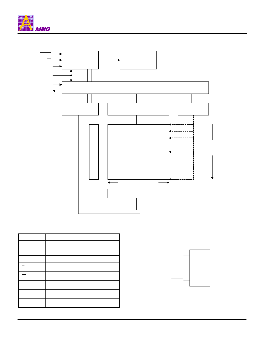
Block Diagram
Control Logic
High Voltage
Generator
I/O Shift Register
Address register
and Counter
256 Byte
Data Buffer
Status
Register
X Decoder
256 Byte (Page Size)
Y Dec
oder
Size of the
read-only
memory area
D
Q
C
000FFh
00000h
HOLD
W
S
FFFFFh
Pin Descriptions
Pin No.
Description
C Serial
Clock
D
Serial Data Input
Q
Serial Data Output
S
Chip Select
W
Write Protect
HOLD
Hold
Vcc
Supply Voltage
Vss
Ground
Logic Symbol
A25L80P
Q
D
S
W
HOLD
V
SS
V
CC
C

A25L80P
(April, 2006, Version 1.1)
3
AMIC Technology Corp.
SIGNAL DESCRIPTION
Serial Data Output (Q).
This output signal is used to transfer
data serially out of the device. Data is shifted out on the falling
edge of Serial Clock (C).
Serial Data Input (D).
This input signal is used to transfer data
serially into the device. It receives instructions, addresses, and
the data to be programmed. Values are latched on the rising
edge of Serial Clock (C).
Serial Clock (C).
This input signal provides the timing of the
serial interface. Instructions, addresses, or data present at
Serial Data Input (D) are latched on the rising edge of Serial
Clock (C). Data on Serial Data Output (Q) changes after the
falling edge of Serial Clock (C).
Chip Select (
S
).
When this input signal is High, the device is
deselected and Serial Data Output (Q) is at high impedance.
Unless an internal Program, Erase or Write Status Register
cycle is in progress, the device will be in the Standby mode
(this is not the Deep Power-down mode). Driving Chip Select
(
S
) Low enables the device, placing it in the active power
mode.
After Power-up, a falling edge on Chip Select (
S
) is required
prior to the start of any instruction.
Hold (
HOLD
).
The Hold (
HOLD
) signal is used to pause any
serial communications with the device without deselecting the
device.
During the Hold condition, the Serial Data Output (Q) is high
impedance, and Serial Data Input (D) and Serial Clock (C) are
Don't Care. To start the Hold condition, the device must be
selected, with Chip Select (
S
) driven Low.
Write Protect (
W
).
The main purpose of this input signal is to
freeze the size of the area of memory that is protected against
program or erase instructions (as specified by the values in the
BP2, BP1 and BP0 bits of the Status Register).
SPI MODES
These devices can be driven by a microcontroller with its SPI
peripheral running in either of the two following modes:
� CPOL=0, CPHA=0
� CPOL=1, CPHA=1
For these two modes, input data is latched in on the rising edge
of Serial Clock (C), and output data is available from the falling
edge of Serial Clock (C).
The difference between the two modes, as shown in Figure 2,
is the clock polarity when the bus master is in Stand-by mode
and not transferring data:
� C remains at 0 for (CPOL=0, CPHA=0)
� C remains at 1 for (CPOL=1, CPHA=1)

A25L80P
(April, 2006, Version 1.1)
4
AMIC Technology Corp.
Figure 1. Bus Master and Memory Devices on the SPI Bus
Bus Master
(ST6, ST7, ST9,
ST10, Other)
SPI Interface with
(CPOL, CPHA)
= (0, 0) or (1, 1)
CS3 CS2 CS1
SPI Memory
Device
C Q D
S
W HOLD
SPI Memory
Device
C Q D
S
W HOLD
SPI Memory
Device
C Q D
S
W HOLD
SDI
SDO
SCK
Note: The Write Protect (
W
) and Hold (
HOLD
) signals should be driven, High or Low as appropriate.
Figure 2. SPI Modes Supported
MSB
MSB
C
C
D
Q
0
0
1
1
CPOL
CPHA