
A26E001A
2M and 256K MaskRAM
(November, 1998, Version 2.1)
AMIC Technology, Inc.
Document Title
2M and 256K MaskRAM
Revision History
Rev. No.
History
Issue Date
Remark
2.0
Final spec release
October 12, 1998
Final
2.1
Change t
OE
speed from 150ns to 200ns
November 20, 1998
A26E001A
2M and 256K MaskRAM
(November, 1998, Version 21)
1
AMIC Technology, Inc.
Features
n
Power supply range: 1.8V to 3.3V
n
Access time: 450 ns (max.)
n
Current:
Low power version: Operating: 4mA (max.)
Standby:
10
�
A (max.)
n
Extended operating temperature range: -25
�
C to 85
�
C
n
Full static operation, no clock or refreshing required
n
All inputs and outputs are CMOS compatible
n
Common I/O using three-state output
n
Data retention voltage: 1.6V (min.)
n
Available in 32-pin TSOP and sTSOP packages
General Description
The A26E001A is a low operating current 262,144 x 8 bit
CMOS MASK ROM and 32,768 x 8 bit CMOS SRAM
integrated into one chip. It operates on a low power
supply voltage from 1.8V to 3.3V, with two chip selects
to enable the MASK ROM or SRAM independently.
Inputs and three-state outputs are CMOS compatible and
allow for direct interfacing with common system bus
structures.
Minimum standby power is drawn by this device when
ROMCE and RAMCE are at a high level, independent
of the other input levels.
Data retention is guaranteed at a power supply voltage
as low as 1.6V.
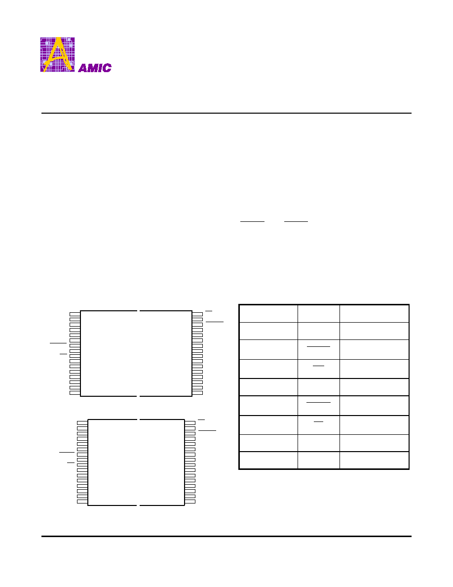
Pin Configuration
Pin Description
Pin No.
Symbol
Description
1 - 6, 10 - 20, 31
A0 - A17
Address Inputs
7
RAMCE
SRAM Enable
9
WE
Write Enable
21 - 23, 25 - 29
D0 - D7
Data Input/Outputs
30
ROMCE
ROM Enable
32
OE
Output Enable
8
VCC
Power Supply
24
GND
Ground
A26E001AV
1
9
32
24
A11
A9
2
3
4
5
6
7
8
10
11
12
13
14
15
16
A8
A13
A14
A17
RAMCE
VCC
WE
A16
A15
A12
A7
A6
A5
A4
31
30
29
28
27
26
25
23
22
21
20
19
18
17
A10
D7
D6
D5
D4
D3
GND
D2
D1
D0
A0
A1
A2
A3
ROMCE
OE
A26E001AX
1
9
32
24
A11
A9
2
3
4
5
6
7
8
10
11
12
13
14
15
16
A8
A13
A14
A17
RAMCE
VCC
WE
A16
A15
A12
A7
A6
A5
A4
31
30
29
28
27
26
25
23
22
21
20
19
18
17
A10
D7
D6
D5
D4
D3
GND
D2
D1
D0
A0
A1
A2
A3
ROMCE
OE
~ ~
~ ~
~ ~
~ ~
A26E001A
(November, 1998, Version 2.1)
2
AMIC Technology, Inc.
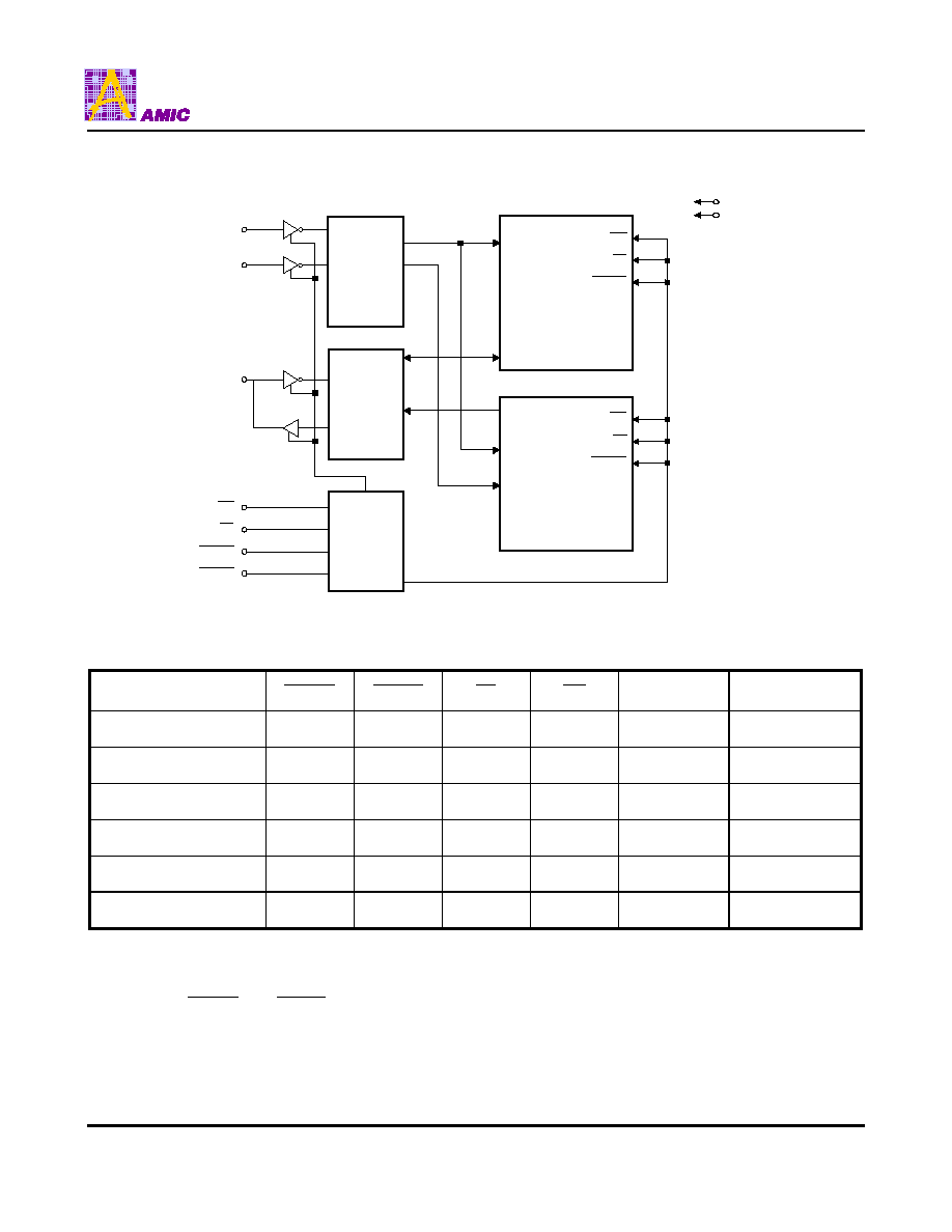
Block Diagram
ADDRESS
BUFFER
DATA
BUFFER
CIRCUIT
CONTROL
CIRCUIT
RAM
A0-A14
D0-D7
D0-D7
A0-A14
A15-A17
ROMCE
OE
WE
RAMCE
OE
WE
ROM
D0 - D7
A15 - A17
A0 - A14
VCC
GND
WE
OE
RAMCE
ROMCE
Truth Table
Mode
ROMCE
RAMCE
OE
WE
D0 - D7
Supply Current
Standby
H
H
X
X
High Z
I
SB
, I
SB1
Output Disable
L
H
H
X
High Z
I
CCR
ROM Read
L
H
L
X
D
OUT
I
CCR
Output Disable
H
L
H
H
High Z
I
CCS
SRAM Read
H
L
L
H
D
OUT
I
CCS
SRAM Write
H
L
X
L
D
IN
I
CCS
Notes:
1. X = H or L
2. A15 - A17 are only valid for ROM.
3. In case that ROMCE and RAMCE are "L" at the same time, both ROM and SRAM will be disabled.

A26E001A
(November, 1998, Version 2.1)
3
AMIC Technology, Inc.
Recommended DC Operating Conditions
(T
A
= -25
�
C to + 85
�
C)
Symbol
Parameter
Min.
Typ.
Max.
Unit
VCC
Supply Voltage
1.8
3.0
3.3
V
GND
Ground
0
0
0
V
V
IH
Input High Voltage
VCC x 0.7
-
VCC + 0.3
V
V
IL
Input Low Voltage
-0.3
-
VCC x 0.3
V
Absolute Maximum Ratings*
VCC to GND . . . . . . . . . . . . . . . . . . . . . . . -0.5V to +4.6V
IN, IN/OUT Volt to GND . . . . . . . . . . -0.5V to VCC + 0.5V
Operating Temperature, Topr . . . . . . . . . -25
�
C to +85
�
C
Storage Temperature, Tstg . . . . . . . . . . -55
�
C to +125
�
C
Power Dissipation, P
T
. . . . . . . . . . . . . . . . . . . . . . . 0.7W
Soldering Temp. & Time . . . . . . . . . . . . . . 260
�
C, 10 sec
*Comments
Stresses above those listed under "Absolute Maximum
Ratings" may cause permanent damage to this device.
These are stress ratings only. Functional operation of
this device at these or any other conditions above those
indicated in the operational sections of this specification
is not implied or intended. Exposure to the absolute
maximum rating conditions for extended periods may
affect device reliability.
DC Electrical Characteristics
(T
A
= -25
�
C to + 85
�
C, VCC = 1.8V to 3.3V)
Symbol
Parameter
Min.
Max.
Unit
Conditions
I
LI
Input Leakage Current
-
1
�
A
V
IN
= GND to VCC
I
LO
Output Leakage Current
-
1
�
A
V
I/O
= GND to VCC
I
CCR
ROM Operating Current
-
4
mA
Min. Cycle, Duty = 100%
ROMCE = V
IL
and RAMCE = V
IH
,
I
I/O
= 0mA, V
IN
= VCC or GND
I
CCS
SRAM Operating Current
-
4
mA
Min. Cycle, Duty = 100%
ROMCE = V
IH
and RAMCE = V
IL
,
I
I/O
= 0mA, V
IN
= VCC or GND
I
SB
-
50
�
A
ROMCE = V
IH
and RAMCE = V
IH
I
SB1
Standby Supply Current
-
10
�
A
ROMCE
VCC - 0.2V and
RAMCE
VCC - o.2V
V
OL
Output Low Voltage
-
0.4
V
I
OL
= 200
�
A
V
OH
Output High Voltage
VCC - 0.4
-
V
I
OH
= -200
�
A
A26E001A
(November, 1998, Version 2.1)
4
AMIC Technology, Inc.
Capacitance
(T
A
= 25
�
C, f = 1.0MHz)
Symbol
Parameter
Min.
Max.
Unit
Conditions
C
I
*
Input Capacitance
6
pF
T
A
= 25
�
C
C
O
*
Input/Output Capacitance
8
pF
f = 1.0MHz
* These parameters are sampled and not 100% tested.
AC Characteristics (ROM/SRAM Selection)
(T
A
= -25
�
C to +85
�
C, VCC = 1.8V to 3.3V)
Symbol
Parameter
Min.
Max.
Unit
t
RTS
ROMCE Disable to RAMCE Enable Time
10
-
ns
t
STR
RAMCE Disable to ROMCE Enable Time
10
-
ns
AC Characteristics (ROM Selected)
(T
A
= -25
�
C to +85
�
C, VCC = 1.8V to 3.3V)
Symbol
Parameter
Min.
Max.
Unit
t
RC
Read Cycle Time
500
-
ns
t
AA
Address Access Time
-
450
ns
t
ACE
ROMCE Chip Enable Access Time
-
450
ns
t
OE
Output Enable to Output Valid
-
200
ns
t
CLZ
ROMCE Chip Enable to Output in Low Z
10
-
ns
t
OLZ
Output Enable to Output in Low Z
10
-
ns
t
CHZ
ROMCE Chip Disable to Output in High Z
-
100
ns
t
OHZ
Output Disable to Output in High Z
-
100
ns
t
OH
Output Hold from Address Change
10
-
ns
Notes: t
CHZ
, and t
OHZ
are defined as the time at which the outputs achieve the open circuit condition and are not referred
to output voltage levels.