A27020 Series
Preliminary
256K X 8 OTP CMOS EPROM
PRELIMINARY (August, 2002, Version 0.0)
1
AMIC Technology, Inc.
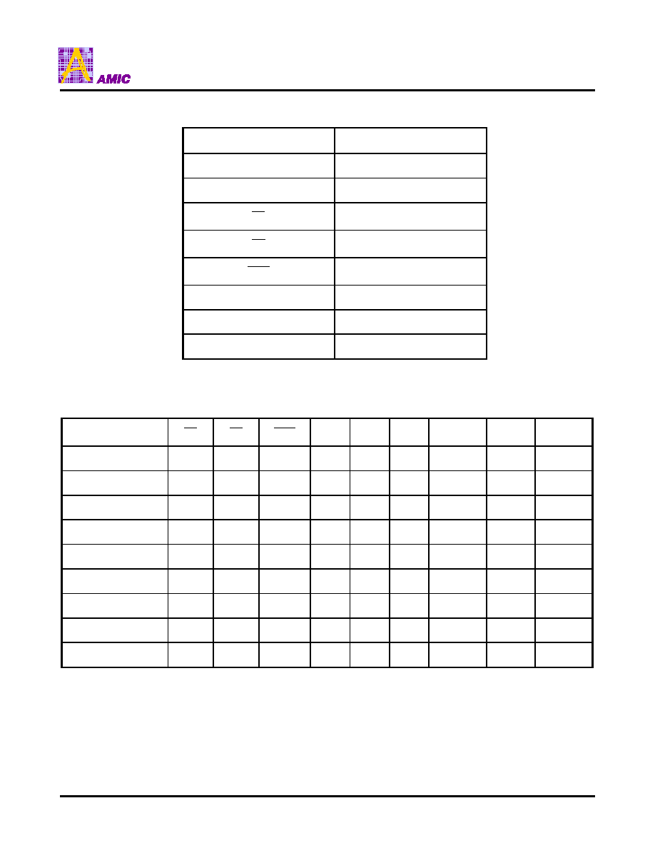
Features
n
262,144 X 8 bit organization
n
Programming voltage: 12.75V
n
Access time: 55/70 ns (max.)
n
Current: Operating: 30mA (max.) at 5MHz
Standby:
100
µ
A (max.)
n
All inputs and outputs are directly TTL-compatible
n
Available in 32-pin DIP and 32-pin PLCC packages
General Description
The A27020 chip is a high-performance 2,097,152 bit
one-time programmable read only memory (OTP
EPROM) organized as 256K by 8 bits. The A27020
requires only 5V power supply in normal read mode
operation and any input signals are TTL levels. The
A27020 is available in industry standard 32 pin dual-in-
line and 32 pin PLCC packages.
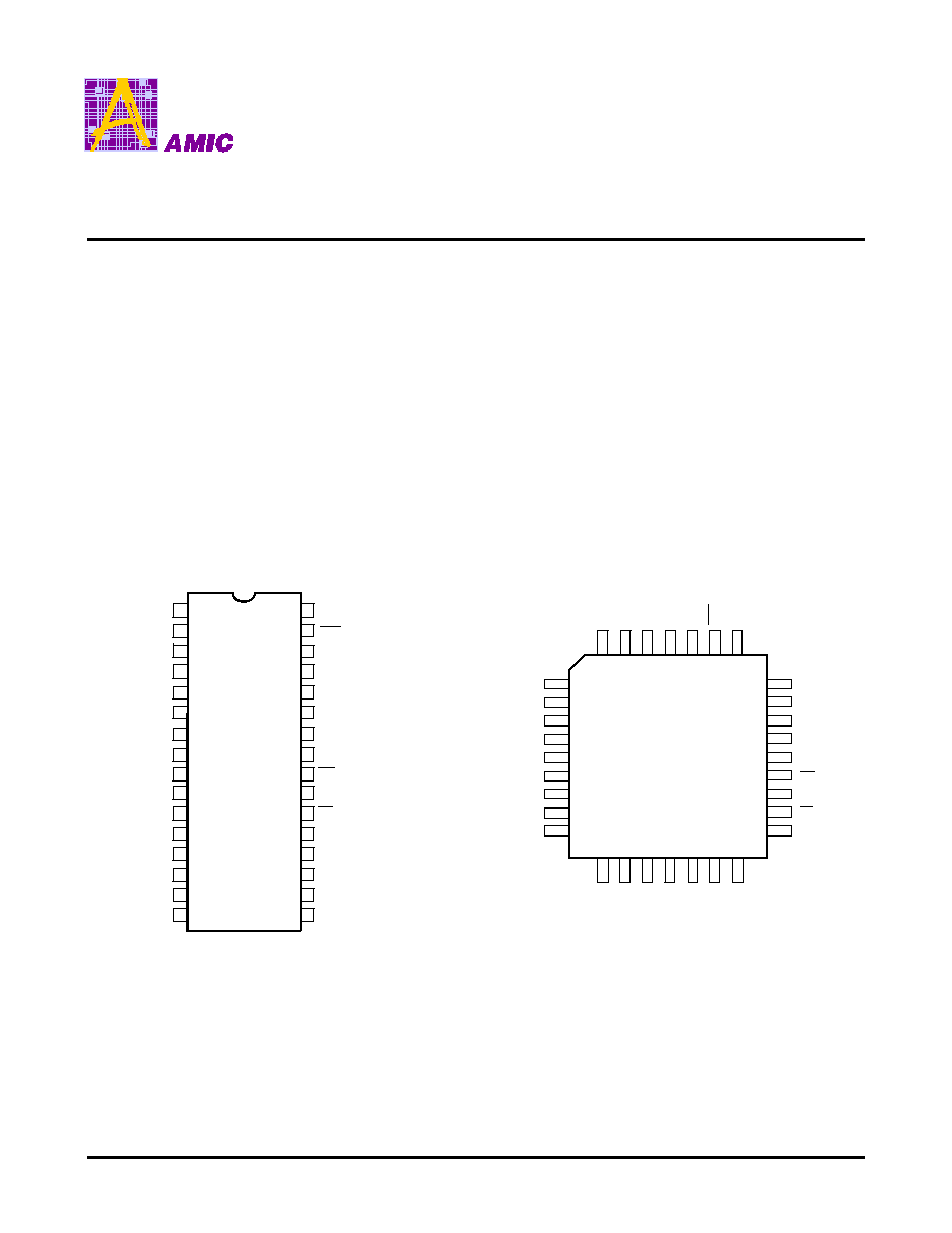
Pin Configurations
n
DIP
n
PLCC
VPP
A16
A15
A12
A7
A6
A5
A4
A3
A2
I/O
0
I/O
1
I/O
3
I/O
4
I/O
5
A11
A9
A13
VCC
A10
A27020
1
2
3
4
5
6
7
8
9
10
11
12
13
14
19
20
21
22
23
24
25
26
27
28
29
30
31
32
A8
I/O
2
GND
I/O
6
I/O
7
CE
A14
18
15
16
17
A1
A0
OE
PGM
A17
A27020L
A7
A9
I/O
7
CE
A6
A5
A4
A3
A2
A1
A0
I/O
0
A8
A13
A14
A12
A15
A16
VPP
VCC
A17
I/O
1
I/O
2
GND
I/O
4
I/O
5
I/O
6
1
2
3
4
5
6
7
8
9
10
11
12
13
32
31
30
14
16
15
17
18
19
20
21
22
23
24
25
26
27
28
29
A11
OE
A10
I/O
3
PGM

A27020 Series
PRELIMINARY (August, 2002, Version 0.0)
3
AMIC Technology, Inc.
Functional Description
Read Mode
The A27020 has two control functions, both of which must
be logically active in order to obtain data at the outputs.
CE is the power control and should be used for device
selection. OE is the output control and should be used to
data to the output pins, which is independent of device
selection. Assuming that addresses are stable, address
access time (t
AA
) is equal to the delay from CE to output
(t
CE
). Data is available at the output after a delay (t
OE
) from
the falling edge of OE , as long as CE has been low and
the addresses have been stable for at least t
ACC
- t
OE
.
Standby Mode
The A27020 has a standby mode which reduces the
active current from 30mA to 100
µ
A. The A27020 is placed
in the standby mode by applying a CMOS high signal to
CE . When in the standby mode, the output are in a high
impedance state, independent of the OE .
Auto Identify Mode
The auto identify mode allows the reading out of a binary
code from a EPROM that will identify its manufacturer and
type. This mode is intended for use by programming
equipment for the purpose of automatically matching the
device to be programmed with its corresponding
programming algorithm.
To activate the mode, the programming equipment must
apply 12.0V
±
0.5V on address line A9 of the A27020.
Three identification code can be read from data output pin
by toggling A0 and A1. The other addresses must be held
at V
IL
during this mode. Byte 0 (with A0 at V
IL
, A1 at V
IL
)
represents the manufacturer code which is 37H. Byte 1
and Byte 2 represent the device code and continuation
code, which is 64H and 7FH respectively. All identifiers for
these codes will possess odd parity, with MSB (IO
7
)
defined the parity bit.
Absolute Maximum Ratings*
Ambient Operating Temperature (T
A
) . . . . -10
°
C to +85
°
C
Storage Temperature Plastic Package (T
STG
) . . . . . . . . . .
. . . . . . . . . . . . . . . . . . . . . . . . . . . . . . . . -55
°
C to 125
°
C
Applied Input Voltage (V
I
):
All Pins Except A9, VPP and VCC . . . . . . . . . . . . . . . .
. . . . . . . . . . . . . . . . . . . . . . . . . . -0.6V to VCC + 0.6V
A9, VPP . . . . . . . . . . . . . . . . . . . . . . . . -0.6V to 13.5V
VCC . . . . . . . . . . . . . . . . . . . . . . . . . . . . -0.6V to 7.0V
Output Voltage (V
O
) . . . . . . . . . . . . -0.6V to 7.0V (Note 1)
*Comments
Stresses above those listed under "Absolute Maximum
Ratings" may cause permanent damage to this device.
These are stress ratings only. Functional operation of this
device at these or any other conditions above those
indicated in the operational sections of this specification
is not implied or intended. Exposure to the absolute
maximum rating conditions for extended periods may
affect device reliability.
Notes:
1. During voltage transitions, the input may undershoot GND to -2.0V for periods less than 20 ns. Maximum DC voltage on
input and I/O may overshoot to VCC + 2.0V for periods less than 20 ns.
2. When transitions, A9 and VPP may undershoot GND to -2.0V for periods less than 20 ns. Maximum DC input voltage
on A9 and VPP is +13.5V which may overshoot to 14.0V for period less than 20 ns.
A27020 Series
PRELIMINARY (August, 2002, Version 0.0)
4
AMIC Technology, Inc.
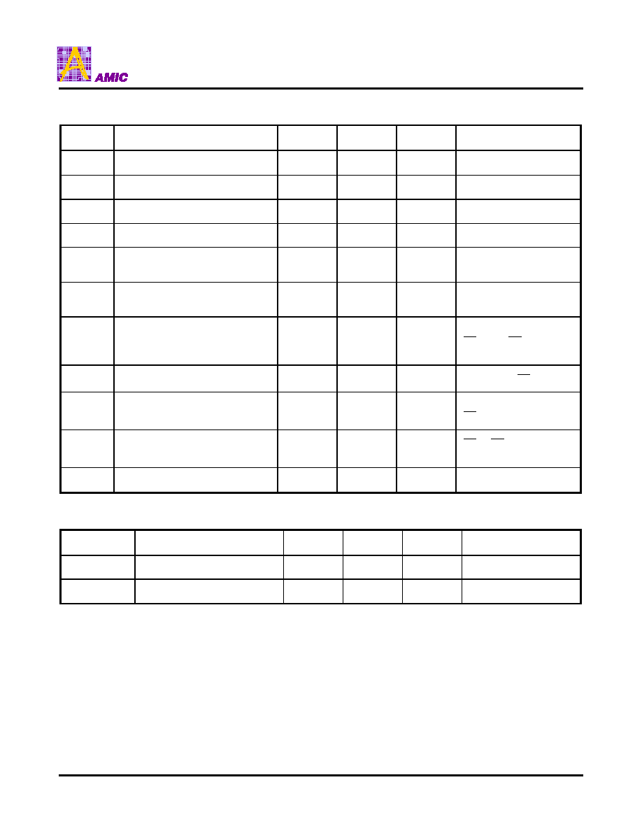
Read Mode DC Electrical Characteristics
(Ta = 0
°
C to 70
°
C, VCC = 5V
±
10%, VPP = VCC)
Symbol
Parameter
Min.
Max.
Unit
Conditions
V
OH
Output High Voltage
2.4
V
I
OH
= -400
µ
A
V
OL
Output Low Voltage
0.4
V
I
OL
= 2.1mA
V
IH
Input High Voltage
2.0
VCC + 0.5
V
V
IL
Input Low Voltage
-0.5
0.8
V
I
LI
Input Leakage Current
-1
+1
µ
A
VCC = max.
Vin = 0V to VCC
I
LO
Output Leakage Current
-1
+1
µ
A
VCC = max.
Vout = 0V to VCC
I
CC
VCC Read Operating Current
30
mA
VCC = max.
CE = V
IL
, OE = V
IL
Iout = 0mA, at 5MHz
I
SB
VCC Standby Current (TTL)
1
mA
VCC = max. CE = V
IH
I
SB1
VCC Standby Current (CMOS)
100
µ
A
VCC = max.
CE = VCC - 0.2V
I
PP
VPP Current During Read
10
µ
A
CE = OE = V
IL
,
VPP = VCC
I
ID
A9 Auto Select Current
100
µ
A
A9 = V
ID
, VCC = max.
Capacitance
(T
A
= 25
°
C, f = 1.0MHz)
Symbol
Parameter
Min.
Max.
Unit
Conditions
C
IN
Input Capacitance
8
pF
V
IN
= 0V
C
Out
Output Capacitance
8
pF
V
Out
= 0V
* These parameters are sampled and not 100% tested.