
A278308A
256K X 8 OTP CMOS EPROM
(October, 2003, Version 1.0)
AMIC Technology, Corp.
Document Title
256K X 8 OTP CMOS EPROM
Revision History
Rev. No. History Issue
Date Remark
0.0 Initial
issue
September 29, 2000
Preliminary
0.1
Change Program Verify VCC to 6.25V
March 14, 2001
1.0
Final version release
October 7, 2003
Final
A278308A
256K X 8 OTP CMOS EPROM
(October, 2003, Version 1.0)
1
AMIC Technology, Corp.
Features
262,144 X 8 bit organization
Programming voltage: 12.75V
Access time: 55/70 ns (max.)
Current: Operating: 30mA (max.) at 5MHz
Standby: 100
µ
A (max.)
All inputs and outputs are directly TTL-compatible
Available in 32-pin DIP and 32-pin PLCC packages
General Description
The A278308A chip is a high-performance 2,097,152 bit
one-time programmable read only memory (OTP EPROM)
organized as 256K by 8 bits. The A278308A requires only
5V power supply in normal read mode operation and any
input signals are TTL levels. The A278308A is available in
industry standard 32 pin dual-in-line and 32 pin PLCC
packages.
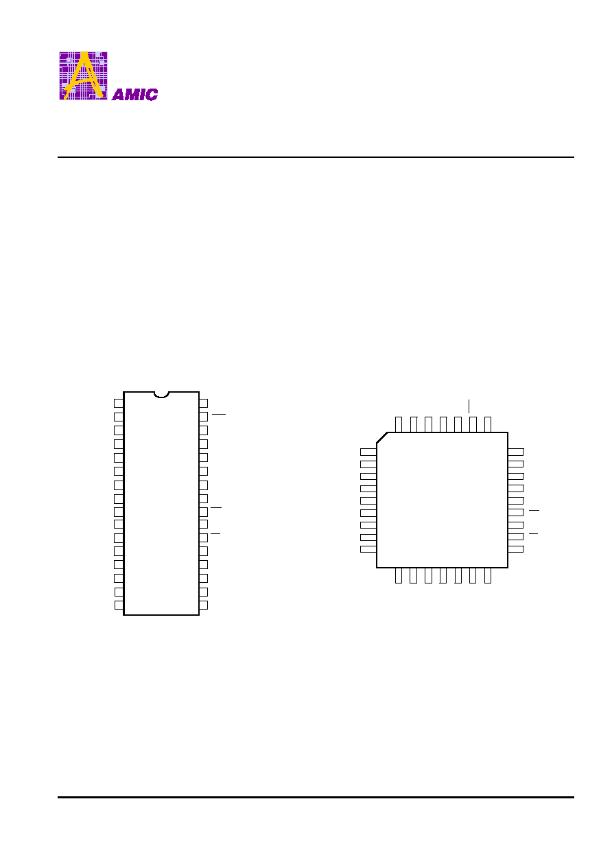
Pin Configurations
DIP
PLCC
VPP
A16
A15
A12
A7
A6
A5
A4
A3
A2
I/O
0
I/O
1
I/O
3
I/O
4
I/O
5
A11
A9
A13
VCC
A10
A278308A
1
2
3
4
5
6
7
8
9
10
11
12
13
14
19
20
21
22
23
24
25
26
27
28
29
30
31
32
A8
I/O
2
GND
I/O
6
I/O
7
CE
A14
18
15
16
17
A1
A0
OE
PGM
A17
A278308AL
A7
A9
I/O
7
CE
A6
A5
A4
A3
A2
A1
A0
I/O
0
A8
A13
A14
A12
A15
A16
VPP
VC
C
A17
I/O
1
I/O
2
GND
I/O
4
I/O
5
I/O
6
1
2
3
4
5
6
7
8
9
10
11
12
13
32
31
30
14
16
15
17
18
19
20
21
22
23
24
25
26
27
28
29
A11
OE
A10
I/O
3
PGM
A278308A
(October, 2003, Version 1.0)
2
AMIC Technology, Corp.
Pin Configurations
Pin Name
Function
A0-A17 Address
Inputs
I/O
7
-I/O
0
Data Inputs / Outputs
CE
Chip Enable
OE
Output Enable
PGM
Program Strobe
VPP
Program Power Supply
VCC Power
Supply
GND Ground
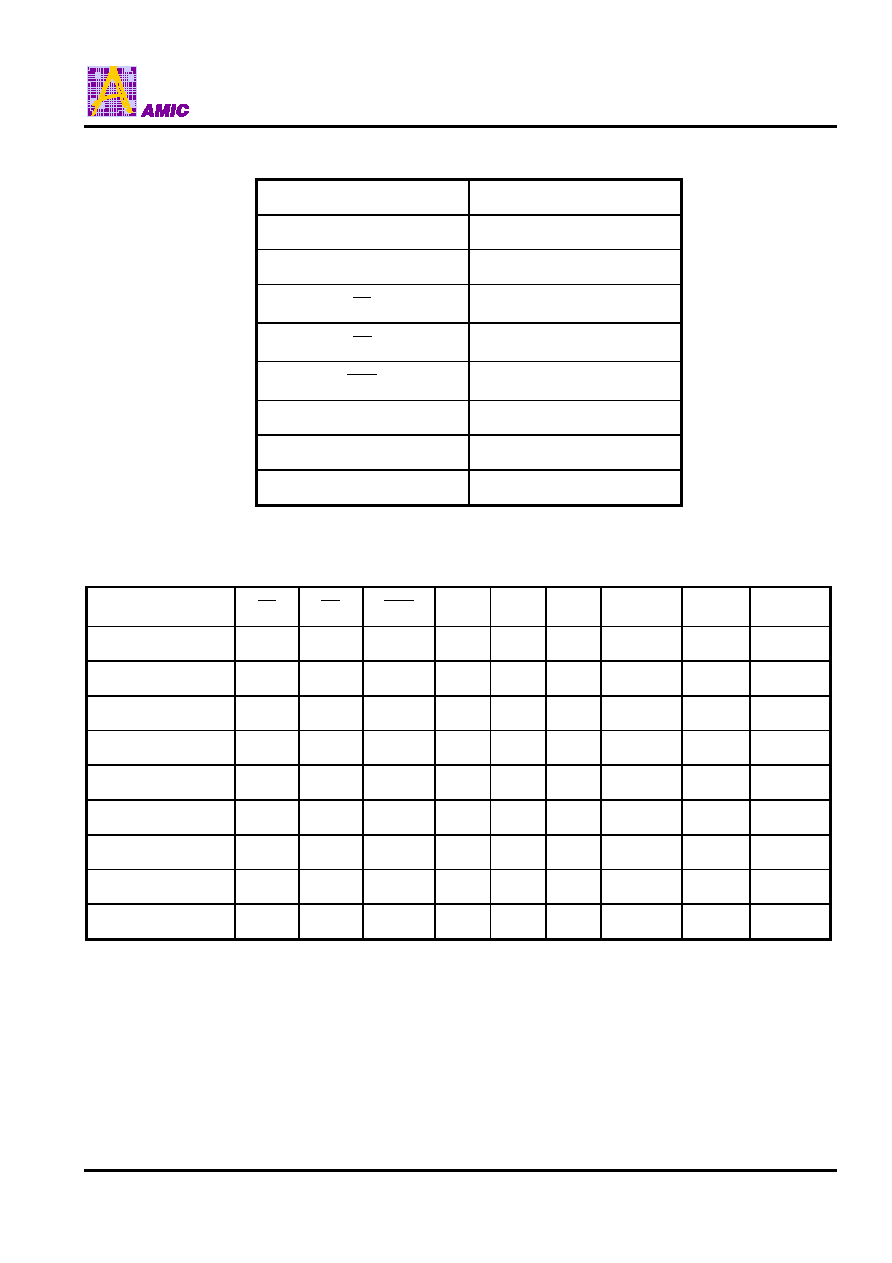
Operating Modes and Truth Table
Mode
CE
OE
PGM
A0 A1 A9 VPP VCC I/O
7
-I/O
0
Read V
IL
V
IL
X X X X VCC VCC
Data
Out
Output Disable
V
IL
V
IH
X X X X VCC VCC Hi-Z
Standby V
IH
X X X X X VCC VCC Hi-Z
Program V
IL
V
IH
V
IL
Pulse
X X X 12.75V
6.25V
Data
In
Program Verify
V
IL
V
IL
V
IH
X X X 12.75V
6.25V
Data
Out
Program Inhibit
V
IH
X X X X X 12.75V 6.25V Hi-Z
Manufacturer Code
(3)
V
IL
V
IL
V
IH
V
IL
V
IL
V
ID
VCC VCC 37H
Device Code
(3)
V
IL
V
IL
V
IH
V
IH
V
IL
V
ID
VCC VCC 64H
Continuation Code
(3)
V
IL
V
IL
V
IH
V
IL
V
IH
V
ID
VCC VCC 7FH
Notes:
1. X = Either V
IH
or V
IL
.
2. V
ID
= 12V
±
0.5V.
3. A2 ~ A8 = A10 ~ A17 = V
IL
(For auto identification)

A278308A
(October, 2003, Version 1.0)
3
AMIC Technology, Corp.
Functional Description
Read Mode
The A278308A has two control functions, both of which
must be logically active in order to obtain data at the
outputs.
CE is the power control and should be used for
device selection. OE is the output control and should
be used to data to the output pins, which is independent
of device selection. Assuming that addresses are stable,
address access time (t
AA
) is equal to the delay from CE
to output (t
CE
). Data is available at the output after a
delay (t
OE
) from the falling edge of OE , as long as CE
has been low and the addresses have been stable for at
least t
ACC
- t
OE
.
Standby Mode
The A278308A has a standby mode which reduces the
active current from 30mA to 100
µ
A. The A278308A is
placed in the standby mode by applying a CMOS high
signal to CE . When in the standby mode, the output are
in a high impedance state, independent of the OE .
Auto Identify Mode
The auto identify mode allows the reading out of a binary
code from a EPROM that will identify its manufacturer
and type. This mode is intended for use by programming
equipment for the purpose of automatically matching the
device to be programmed with its corresponding
programming algorithm.
To activate the mode, the programming equipment must
apply 12.0V
±
0.5V on address line A9 of the A278308A.
Three identification code can be read from data output
pin by toggling A0 and A1. The other addresses must be
held at V
IL
during this mode. Byte 0 (with A0 at V
IL
, A1 at
V
IL
) represents the manufacturer code which is 37H.
Byte 1 and Byte 2 represent the device code and
continuation code, which is 64H and 7FH respectively.
All identifiers for these codes will possess odd parity,
with MSB (IO
7
) defined the parity bit.
Absolute Maximum Ratings*
Ambient Operating Temperature (T
A
) . . . -10
∞
C to +85
∞
C
Storage Temperature Plastic Package (T
STG
) . . . . . . . . .
. . . . . . . . . . . . . . . . . . . . . . . . . . . . . . . . -55
∞
C to 125
∞
C
Applied Input Voltage (V
I
):
All Pins Except A9, VPP and VCC . . . . . . . . . . . . . . . .
. . . . . . . . . . . . . . . . . . . . . . . . . .-0.6V to VCC + 0.6V
A9, VPP . . . . . . . . . . . . . . . . . . . . . . . -0.6V to 13.5V
VCC . . . . . . . . . . . . . . . . . . . . . . . . . . . -0.6V to 7.0V
Output Voltage (V
O
) . . . . . . . . . . . -0.6V to 7.0V (Note 1)
*Comments
Stresses above those listed under "Absolute Maximum
Ratings" may cause permanent damage to this device.
These are stress ratings only. Functional operation of
this device at these or any other conditions above those
indicated in the operational sections of this specification
is not implied or intended. Exposure to the absolute
maximum rating conditions for extended periods may
affect device reliability.
Notes:
1. During voltage transitions, the input may undershoot GND to -2.0V for periods less than 20 ns. Maximum DC voltage on
input and I/O may overshoot to VCC + 2.0V for periods less than 20 ns.
2. When transitions, A9 and VPP may undershoot GND to -2.0V for periods less than 20 ns. Maximum DC input voltage
on A9 and VPP is +13.5V which may overshoot to 14.0V for period less than 20 ns.
A278308A
(October, 2003, Version 1.0)
4
AMIC Technology, Corp.
Read Mode DC Electrical Characteristics
(Ta = 0
∞
C to 70
∞
C, VCC = 5V
±
10%, VPP = VCC)
Symbol Parameter Min.
Max.
Unit
Conditions
V
OH
Output High Voltage
2.4
V
I
OH
= -400
µ
A
V
OL
Output Low Voltage
0.4
V
I
OL
= 2.1mA
V
IH
Input High Voltage
2.0
VCC + 0.5
V
V
IL
Input Low Voltage
-0.5
0.8
V
I
LI
Input Leakage Current
-1
+1
µ
A
VCC = max.
Vin = 0V to VCC
I
LO
Output Leakage Current
-1
+1
µ
A
VCC = max.
Vout = 0V to VCC
I
CC
VCC Read Operating Current
30
mA
VCC = max.
CE = V
IL
, OE = V
IL
Iout = 0mA, at 5MHz
I
SB
VCC Standby Current (TTL)
1
mA
VCC = max. CE = V
IH
I
SB1
VCC Standby Current (CMOS)
100
µ
A
VCC = max.
CE = VCC - 0.2V
I
PP
VPP Current During Read
10
µ
A
CE = OE = V
IL
,
VPP = VCC
I
ID
A9 Auto Select Current
100
µ
A
A9 = V
ID
, VCC = max.
Capacitance
(T
A
= 25
∞
C, f = 1.0MHz)
Symbol Parameter Min.
Max.
Unit
Conditions
C
IN
Input
Capacitance
8 pF
V
IN
= 0V
C
Out
Output
Capacitance
8 pF
V
Out
= 0V
* These parameters are sampled and not 100% tested.

A278308A
(October, 2003, Version 1.0)
5
AMIC Technology, Corp.
Read Mode AC Characteristics
(Ta = 0
∞
C to 70
∞
C, VCC = 5V
±
10%, VPP = VCC)
Symbol Parameter
55ns 70ns
Unit
Min. Max. Min. Max.
t
CYC
Cycle
Time
55 70 ns
t
AA
Address
Access
Time
55 70
ns
t
CE
Chip Enable Access Time
55
70
ns
t
OE
Output Enable Access Time
30
35
ns
t
OH
Output Hold after Address, CE or OE , whichever
Occurred First
0 0
ns
t
HZ
Output High Z Delay
20
20
ns
Read Mode Switching Waveforms
t
OH
t
HZ
High-Z
t
AA
t
OE
t
CE
Valid
Output
Address Valid
ADDRESS
CE
OE
OUTPUT
t
CYC
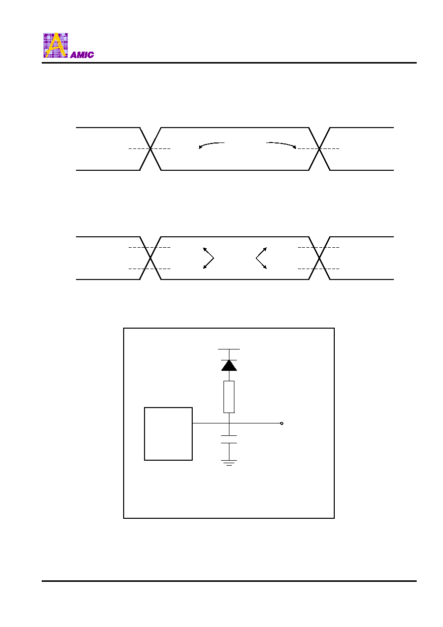
A278308A
(October, 2003, Version 1.0)
6
AMIC Technology, Corp.
AC Measurement Conditions
for 55 ns
Input Rise and Fall Times
10 ns
Input Pulse Voltage: 0V to 3Volt
Input and Output Timing Ref. Voltage: 1.5Volt
3.0V
0V
1.5V
1.5V
TEST
POINTS
INPUT
OUTPUT
for 70 ns
Input Rise and Fall Times
10 ns
Input Pulse Voltage: 0.4V to 2.4Volt
Input and Output Timing Ref. Voltage: 0.8V to 2.0Volt
2.4V
0.4V
2.0V
2.0V
TEST
POINTS
INPUT
OUTPUT
0.8V
0.8V
AC Testing Load Circuit
C
L
= 30pF or 100pF
OUT
3.3K
1N914
1.3V
DEVICE
UNDER
TEST
C
L
= 30pF for 55 ns
C
L
= 100pF for 70/90 ns
C
L
includes JIG capacitance
A278308A
(October, 2003, Version 1.0)
7
AMIC Technology, Corp.
Programming and Program Verify
The programming flowchart is shown in Page 10.
The A278308A is shipped with all bits being set to "1".
Programming causes relevant bits to be changed to "0".
The programming mode is started by setting VCC to
+6.25V and VPP to +12.75V, while CE and PGM are at
V
IL
, and OE is at V
IH
. Data to be programmed can be
directly input in the 8 bit format through the data bus.
The write programming algorithm reduces programming
time by using 100
µ
s pulse followed by a byte verification
to determine whether the byte has been successfully
programmed. If the data does not pass the verification, an
additional pulse programming is applied for a maximum of
25 pulses. On completion of 1 byte programming and, The
verified address is incremented. After the final address is
completed, all bytes are verified again with VCC = 5.0
Volt.
Program Inhibit
This mode is used to program one of multiple A278308A
whose OE , PGM , VPP, VCC, address bus and data bus
are connected in parallel. When programming is
performed, other A278308A can be inhibited from being
programmed by setting their CE pins to V
IH
.
Programming Mode DC Characteristics
(Ta = 0
∞
C to 70
∞
C, VCC = 6.25V
±
0.25V, VPP = 12.75V
±
0.25V)
Symbol Parameter Min.
Max.
Unit Test
Conditions
V
OH
Output High Voltage
2.4
V
I
OH
= -400
µ
A
V
OL
Output Low Voltage
0.4
V
I
OL
= 2.1mA
V
IH
Input High Voltage
2.0
VCC + 0.5
V
V
IL
Input Low Voltage
-0.5
0.8
V
I
LI
Input Leakage Current
-1
+1
µ
A
VCC = max. Vin = 0V to VCC
I
CC
VCC Current During Program
50
mA
I
PP
VPP Current During Program
50
mA
CE = V
IL
V
ID
A9 Auto Select Voltage
11.5
12.5
V
A9 = V
ID
VCC1
Programming Supply Voltage
6.0
6.5
V
VPP1 Programming
Voltage
12.5
13
V
Note: VCC must be applied simultaneously or before VPP and removed simultaneously or after VPP.

A278308A
(October, 2003, Version 1.0)
8
AMIC Technology, Corp.
Programming Mode AC Characteristics
(Ta = 0
∞
C to 70
∞
C, VCC= 6.25V
±
0.25V, VPP = 12.75V
±
0.25V)
Symbol Parameter
Min.
Max.
Unit
t
AS
Address Valid to Program Low
2
µ
s
t
DS
Input Valid to Program Low
2
µ
s
t
VPS
VPP High to Program Low
2
µ
s
t
VCS
VCC High to Program Low
2
µ
s
t
CES
CE Low to Program Low
2
µ
s
t
PW
Program Pulse Width
95
105
µ
s
t
DH
Program High to Input transition
2
µ
s
t
OES
Input Transition to OE Low
2
µ
s
t
OE
OE Low to Output Valid
100 ns
t
OHZ
OE High to Output Hi-Z
130 ns
t
AH
OE High to Address Transition
0 ns

A278308A
(October, 2003, Version 1.0)
9
AMIC Technology, Corp.
Programming and Verify Mode AC Waveforms
t
OES
t
PW
t
CES
t
VCS
t
VPS
t
DS
t
AS
PROGRAM
PROGRAM VERIFY
VALID
DATA IN
DATA OUT
t
DH
t
OE
t
OHZ
t
AH
ADDRESS
DATA
VPP
VCC
CE
PGM
OE
V
IH
V
IL
V
IH
V
IH
VCC
VCC1
VCC
VPP1
V
IL
V
IH
V
IL
V
IL

A278308A
(October, 2003, Version 1.0)
10
AMIC Technology, Corp.
Programming Flowchart
START
ADDRESS=FIRST LOCATION
VCC=6.25V
VPP=12.75V
X = 0
PROGRAM ONE 100 s PULSE
INCREMENT X
X = 25?
VERIFY BYTE
LAST ADDRESS
VCC=VPP=5.0V
VERIFY ALL
BYTES ?
DEVICE PASSED
DEVICE FAILED
INCREMENT ADDRESS
FAIL
NO
YES
NO
PASS
YES
FAIL
PASS
VERIFY BYTE
PASS
FAIL
VERIFY
SECTION
INTERACTIVE
SECTION

A278308A
(October, 2003, Version 1.0)
11
AMIC Technology, Corp.
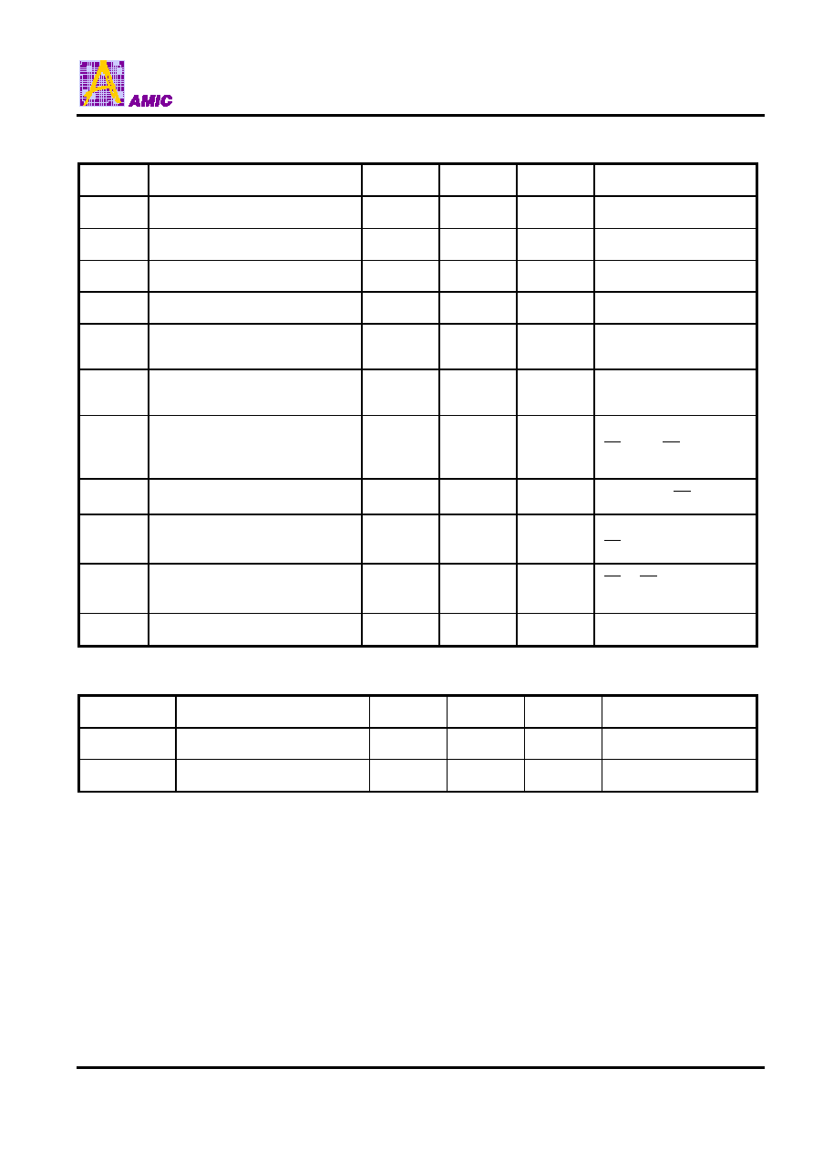
Ordering Information
Part No.
Access Time (ns)
Operating Current
Max. (mA) at 5MHz
Standby Current
Max. (
µ
A)
Package
A278308A-55
55
30
100
32Pin DIP
A278308AL-55 55
30
100 32Pin
PLCC
A278308A-70 70
30 100 32Pin
DIP
A278308AL-70 70
30
100 32Pin
PLCC
A278308A
(October, 2003, Version 1.0)
12
AMIC Technology, Corp.
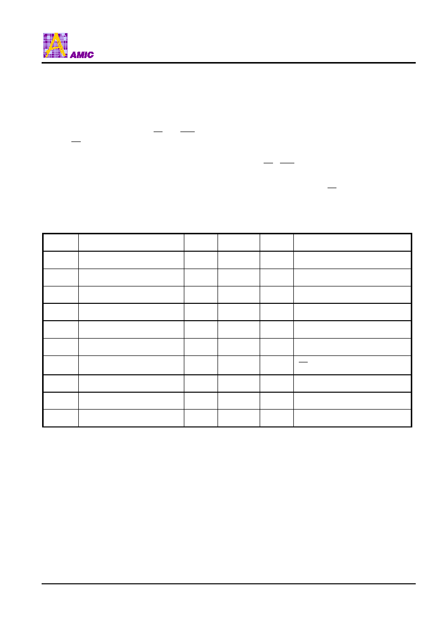
Package Information
P-DIP 32L Outline Dimensions
unit: inches/mm
1
32
E
A
2
A
L
E
1
E
A
D
C
B
1
B
A
1
Base Plane
Seating Plane
16
17
e
Dimensions in inches
Dimensions in mm
Symbol
Min Nom
Max Min Nom
Max
A - -
0.210
- -
5.334
A
1
0.015
- -
0.381
- -
A
2
0.149
0.154
0.159
3.785
3.912
4.039
B
- 0.018
- - 0.457
-
B
1
- 0.050
- - 1.270
-
C
- 0.010
- - 0.254
-
D 1.645
1.650
1.655
41.783
41.91
42.037
E 0.537
0.542
0.547
13.64
13.767
13.894
E
1
0.590
0.600
0.610
14.986
15.240
15.494
E
A
0.630
0.650
0.670
16.002
16.510
17.018
e
- 0.100
- - 2.540
-
L 0.120
0.130
0.140
3.048
3.302
3.556
0
∞
-
15
∞
0
∞
-
15
∞
Notes:
1. The maximum value of dimension D includes end flash.
2. Dimension E does not include resin fins.
A278308A
(October, 2003, Version 1.0)
13
AMIC Technology, Corp.
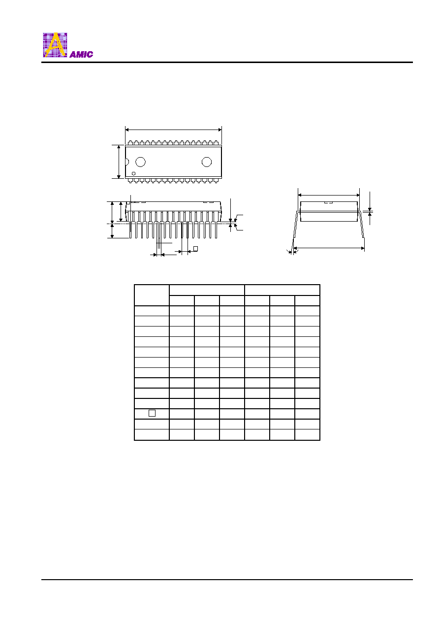
Package Information
PLCC 32L Outline Dimension
unit: inches/mm
A
1
A
2
A
e
D
y
H
D
D
13
G
D
b
1
b
G
E
c
5
14
20
21
29
30
32
1
4
E
H
E
L
Dimensions in inches
Dimensions in mm
Symbol
Min Nom
Max Min Nom
Max
A - -
0.134
- -
3.40
A
1
0.0185
- - 0.47
- -
A
2
0.105
0.110
0.115
2.67
2.80
2.93
b
1
0.026
0.028
0.032
0.66
0.71
0.81
b 0.016
0.018
0.021
0.41
0.46
0.54
C 0.008
0.010
0.014
0.20
0.254
0.35
D 0.547
0.550
0.553
13.89
13.97
14.05
E 0.447
0.450
0.453
11.35
11.43
11.51
e 0.044
0.050
0.056
1.12
1.27
1.42
G
D
0.490
0.510
0.530
12.45
12.95
13.46
G
E
0.390
0.410
0.430
9.91
10.41
10.92
H
D
0.585
0.590
0.595
14.86
14.99
15.11
H
E
0.485
0.490
0.495
12.32
12.45
12.57
L 0.075
0.090
0.095
1.91
2.29
2.41
y
- -
0.003
- -
0.075
0
∞
- 10
∞
0
∞
- 10
∞
Notes:
1. Dimensions D and E do not include resin fins.
2. Dimensions G
D
& G
E
are for PC Board surface mount pad pitch
design reference only.