Microsoft Word - LP621024D-T.doc

LP621024D-T Series
128K X 8 BIT CMOS SRAM
(August, 2004, Version 1.1)
AMIC Technology, Corp.
Document Title
128K X 8 BIT CMOS SRAM
Revision History
Rev. No. History Issue
Date Remark
1.1
Add Pb-Free package type
August 19, 2004
Final
LP621024D-T Series
128K X 8 BIT CMOS SRAM
(August, 2004, Version 1.1)
1
AMIC Technology, Corp.
Features
Single +5V power supply
Access times: 55/70 ns (max.)
Current:
Very low power version: Operating: 70mA (max.)
Standby: 50
µ
A (max.)
Full static operation, no clock or refreshing required
All inputs and outputs are directly TTL-compatible
Common I/O using three-state output
Output enable and two chip enable inputs for easy
application
Data retention voltage: 2V (min.)
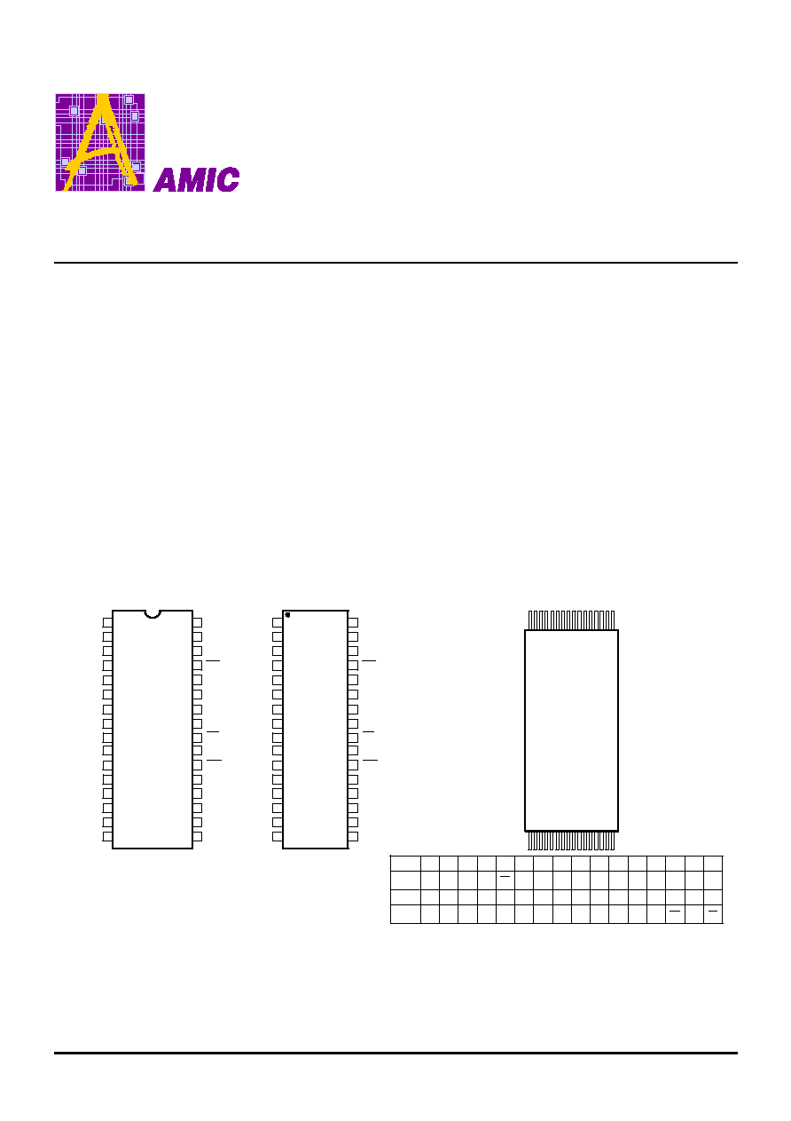
Available in 32-pin DIP, SOP TSOP and TSSOP
(8 X 13.4mm) packages
General Description
The LP621024D-T is a low operating current 1,048,576-bit
static random access memory organized as 131,072 words
by 8 bits and operates on a single 5V power supply.
Inputs and three-state outputs are TTL compatible and
allow for direct interfacing with common system bus
structures.
Two chip enable inputs are provided for POWER-DOWN
and device enable and an output enable input is included
for easy interfacing.
Data retention is guaranteed at a power supply voltage as
low as 2V.
Pin Configurations
DIP
SOP
TSOP/(TSSOP)
NC
A16
A14
A12
A7
A6
A5
A4
A3
A2
A1
A0
I/O
1
I/O
2
I/O
3
I/O
4
GND
I/O
5
I/O
6
I/O
7
I/O
8
A10
A9
A8
A13
CE2
A15
VCC
A11
LP621024D-T
1
2
3
4
5
6
7
8
9
10
11
12
13
14
15
16
17
18
19
20
21
22
23
24
25
26
27
28
29
30
31
32
OE
NC
A16
A14
A12
A7
A6
A5
A4
A3
A2
A1
A0
I/O
1
I/O
2
I/O
3
I/O
4
GND
I/O
5
I/O
6
I/O
7
I/O
8
A10
A9
A8
A13
CE2
A15
VCC
A11
LP621024DM-T
1
2
3
4
5
6
7
8
9
10
11
12
13
14
15
16
17
18
19
20
21
22
23
24
25
26
27
28
29
30
31
32
OE
LP621024DV-T
(LP621024DX-T)
1
16
17
32
Pin No.
Pin
Name
Pin No.
Pin
Name
1
2
A9
3
4
5
6
7
8
9
10
11
12
13
14
30
29
28
27
26
25
24
22
19
21
20
23
18
17
A8
A13
CE2
A15
VCC
NC
I/O
8
A16
A14
A12
A7
A6
A3
A2
A1
A0
I/O
1
I/O
2
GND
I/O
4
I/O
5
I/O
6
I/O
7
I/O
3
A11
WE
CE1
15
16
31
32
A5
A4
A10
OE
CE1
WE
CE1
WE
LP621024D-T Series
(August, 2004, Version 1.1)
2
AMIC Technology, Corp.
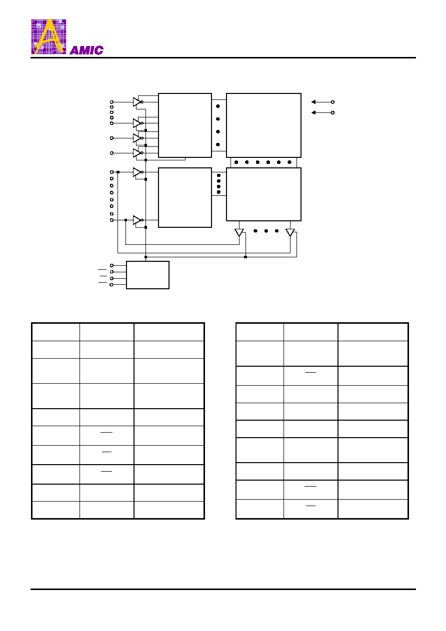
Block Diagram
ROW
DECODER
512 X 2048
MEMORY ARRAY
INPUT DATA
CIRCUIT
COLUMN I/O
CONTROL
CIRCUIT
CE2
CE1
WE
I/O
8
I/O
1
A16
A15
A14
A0
VCC
GND
OE
Pin Descriptions - DIP/SOP
Pin No.
Symbol
Description
1 NC
No
Connection
2 - 12, 23,
25 - 28, 31
A0 - A16
Address Inputs
13 - 15,
17 - 21
I/O
1
- I/O
8
Data
Input/Outputs
16 GND
Ground
22
CE1
Chip Enable
24
OE
Output Enable
29
WE
Write Enable
30 CE2
Chip
Enable
32
VCC
Power Supply (+5V)
Pin Description - TSOP/TSSOP
Pin No.
Symbol
Description
1 - 4, 7,
10 - 20, 31
A0 - A16
Address Inputs
5
WE
Write Enable
6 CE2
Chip
Enable
8 VCC
Power
Supply
9 NC
No
Connection
21 - 23,
25 - 29
I/O
1
- I/O
8
Data
Input/Outputs
24 GND
Ground
30
CE1
Chip Enable
32
OE
Output Enable
LP621024D-T Series
(August, 2004, Version 1.1)
3
AMIC Technology, Corp.
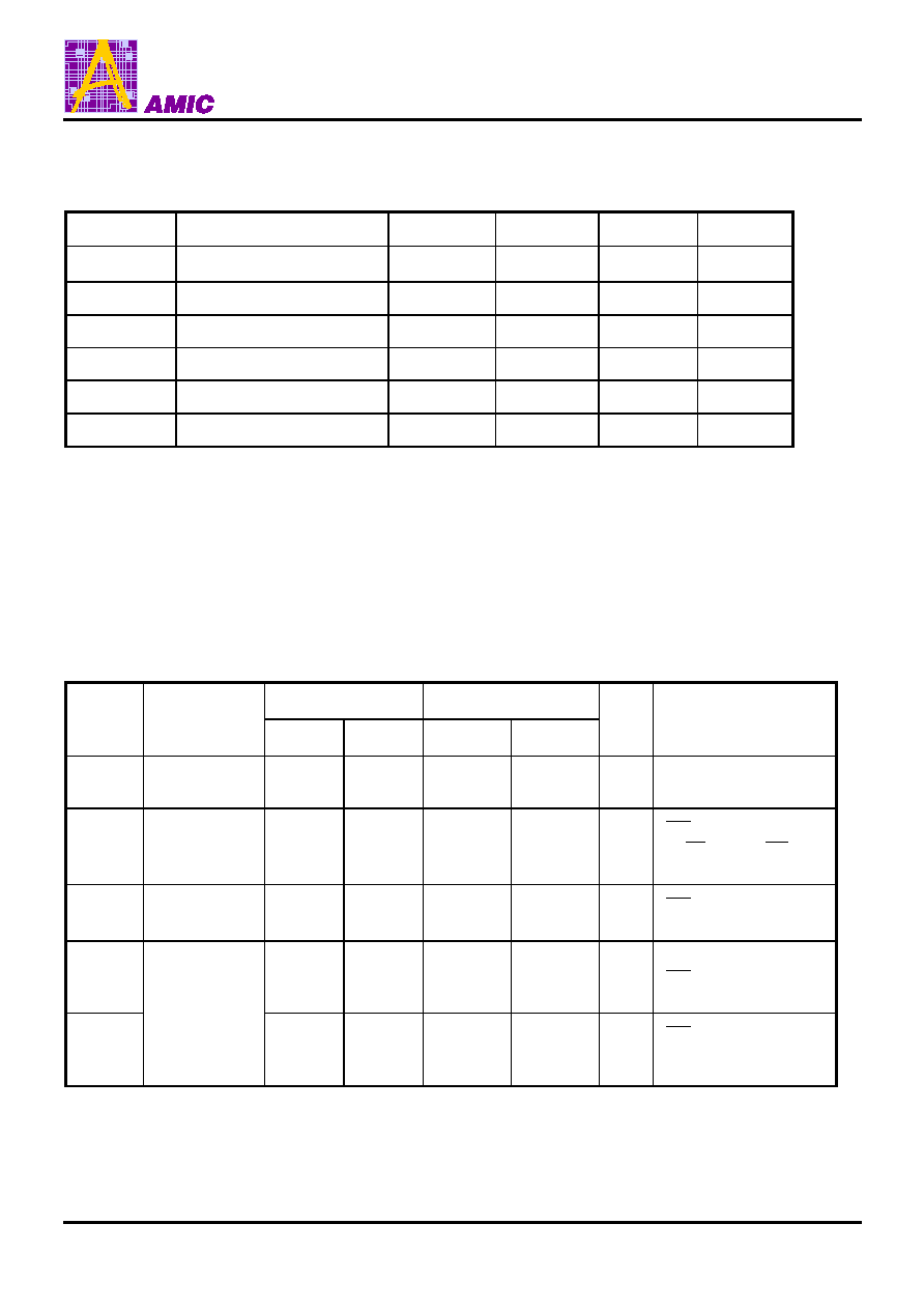
Recommended DC Operating Conditions
(T
A
= -25
°
C to + 85
°
C)
Symbol Parameter Min.
Typ.
Max.
Unit
Supply Voltage
4.5
5.0 5.5 V
GND Ground
0
0
0
V
V
IH
Input High Voltage
2.2
3.5
VCC + 0.3
V
V
IL
Input Low Voltage
-0.3
0
+0.8
V
C
L
Output
Load
-
-
30 pF
TTL Output
Load
-
-
1
-
Absolute Maximum Ratings*
VCC to GND ..............................................-0.5V to + 7.0V
IN, IN/OUT Volt to GND.................... -0.5V to VCC + 0.5V
Operating Temperature, Topr .................. -25
°
C to + 85
°
C
Storage Temperature, Tstg.................... -55
°
C to + 125
°
C
Temperature Under Bias, Tbias............... -10
°
C to + 85
°
C
Power Dissipation, P
T........................................................................
0.7W
Soldering Temp. & Time ............................. 260
°
C, 10 sec
*Comments
Stresses above those listed under "Absolute Maximum
Ratings" may cause permanent damage to this device.
These are stress ratings only. Functional operation of this
device at these or any other conditions above those
indicated in the operational sections of this specification is
not implied or intended. Exposure to the absolute maximum
rating conditions for extended periods may affect device
reliability.
DC Electrical Characteristics
(T
A
= -25
°
C to + 85
°
C, VCC = 5V
±
10%, GND = 0V)
Symbol Parameter
LP621024D-55LLT LP621024D-70LLT
Unit
Conditions
Min.
Max.
Min.
Max.
I
LI
Input Leakage
Current
- 1 - 1
µ
A
V
IN
= GND to VCC
I
LO
Output Leakage
Current
- 1 - 1
µ
A
CE1 = V
IH
or CE2 = V
IL
or OE = V
IH
or WE = V
IL
V
I/O
= GND to VCC
I
CC
Active Power
Supply Current
- 15 - 15
mA
CE1 = V
IL
, CE2 = V
IH
I
I/O
= 0mA
I
CC1
Dynamic
Operating
- 70 - 70
mA
Min. Cycle, Duty = 100%
CE1 = V
IL
, CE2 = V
IH
I
I/O
= 0mA
I
CC2
Current
- 15 - 15
mA
CE1 = V
IL
, CE2 = V
IH
V
IH
= VCC, V
IL
= 0V
f = 1MH
Z,
I
I/O
= 0mA
LP621024D-T Series
(August, 2004, Version 1.1)
4
AMIC Technology, Corp.
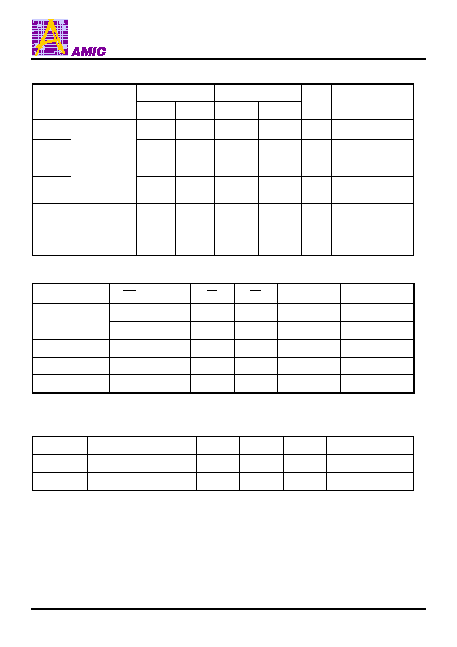
DC Electrical Characteristics (continued)
Symbol Parameter
LP621024D-55LLT LP621024D-70LLT
Unit Conditions
Min.
Max.
Min.
Max.
I
SB
-
2
-
2
mA
CE1 = V
IH
or CE2 =V
IL
I
SB1
Standby
Power
Supply Current
- 50 - 50
µ
A
CE1
VCC - 0.2V
CE2
VCC - 0.2V
V
IN
0V
I
SB2
-
50
-
50
µ
A
CE2
0.2V
V
IN
0V
V
OL
Output Low
Voltage
- 0.4 - 0.4
V
I
OL
= 2.1mA
V
OH
Output High
Voltage
2.4 - 2.4 - V
I
OH
= -1.0mA
Truth Table
Mode
CE1
CE2
OE
WE
I/O Operation
Supply Current
Standby
H X X X High
Z I
SB
, I
SB1
X
L
X
X
High
Z
I
SB
, I
SB2
Output Disable
L
H
H
H
High Z
I
CC,
I
CC1,
I
CC2
Read L
H
L
H
D
OUT
I
CC,
I
CC1,
I
CC2
Write L
H
X
L
D
IN
I
CC,
I
CC1,
I
CC2
Note: X = H or L
Capacitance
(T
A
= 25
°
C, f = 1.0MHz)
Symbol Parameter Min.
Max.
Unit
Conditions
C
IN
* Input
Capacitance
6 pF V
IN
= 0V
C
I/O
* Input/Output
Capacitance 8 pF
V
I/O
= 0V
* These parameters are sampled and not 100% tested.