PRELIMINARY
This document contains information on a product under development at Advanced Micro Devices. The information
is intended to help you evaluate this product. AMD reserves the right to change or discontinue work on this proposed
product without notice.
Publication# 20380
Rev: B Amendment/0
Issue Date: April 1997
5.0 V-only Flash
Am29F400AT/Am29F400AB
4 Megabit (524,288 x 8-Bit/262,144 x 16-Bit) CMOS 5.0 Volt-only,
Sector Erase Flash Memory
DISTINCTIVE CHARACTERISTICS
s
5.0 V
±
10% for read and write operations
-- Minimizes system level power requirements
s
Compatible with JEDEC-standards
-- Pinout and software compatible with
single-power-supply flash
-- Superior inadvertent write protection
s
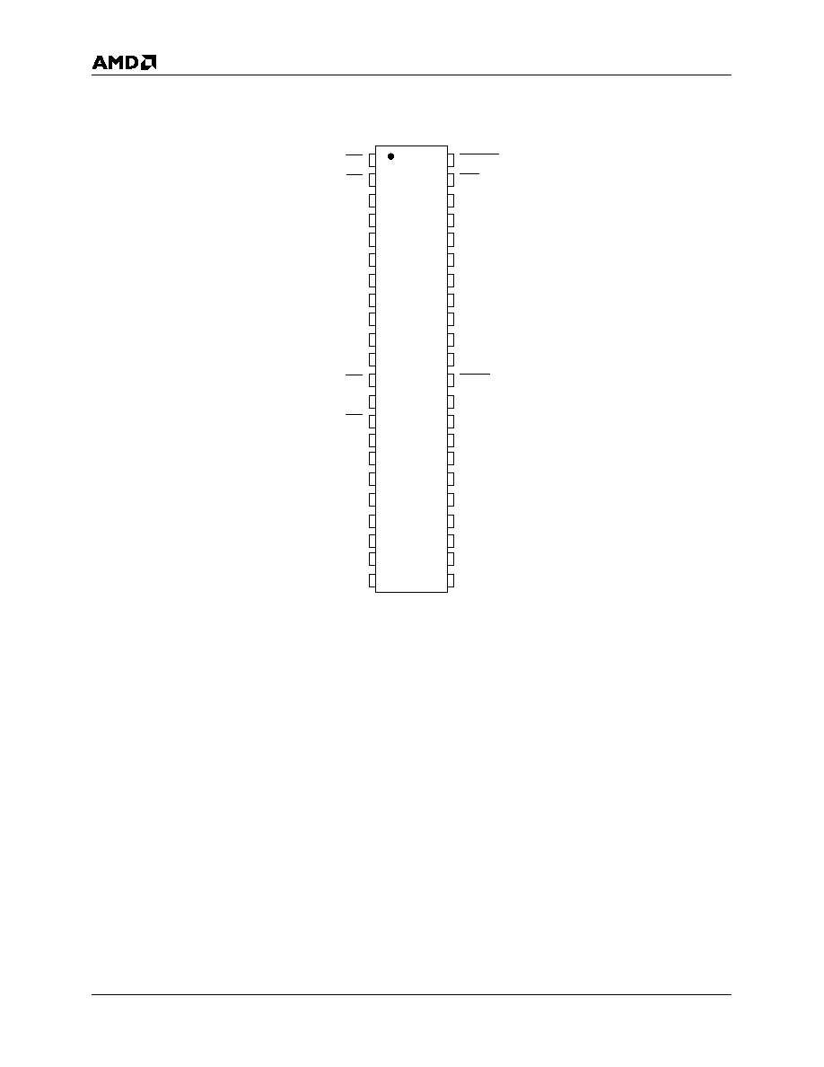
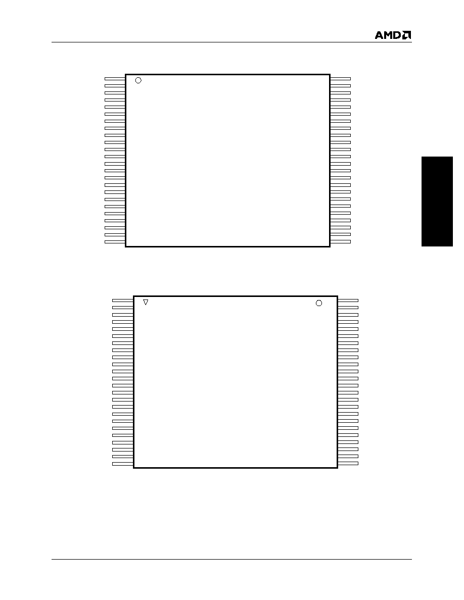
Package options
-- 44-pin SO
-- 48-pin TSOP
s
Minimum 100,000 write/erase cycles guaranteed
s
High performance
-- 60 ns maximum access time
s
Sector erase architecture
-- One 16 Kbyte, two 8 Kbytes, one 32 Kbyte, and
seven 64 Kbytes
-- Any combination of sectors can be erased. Also
supports full chip erase.
s
Sector protection
-- Hardware method that disables any combination
of sectors from write or erase operations.
Implemented using standard PROM
programming equipment.
s
Embedded Erase
TM
Algorithms
-- Automatically preprograms and erases the chip
or any sector
s
Embedded Program
TM
Algorithms
-- Automatically programs and verifies data at
specified address
s
Data Polling and Toggle Bit feature for detection
of program or erase cycle completion
s
Ready/Busy output (RY/BY)
-- Hardware method for detection of program or
erase cycle completion
s
Erase Suspend/Resume
-- Supports reading data from a sector not being
erased
s
Low power consumption
-- 20 mA typical active read current for Byte Mode
-- 28 mA typical active read current for Word Mode
-- 30 mA typical program/erase current
s
Enhanced power management for standby
mode
-- 1
µ
A typical standby current
s
Boot Code Sector Architecture
-- T = Top sector
-- B = Bottom sector
s
Hardware RESET pin
-- Resets internal state machine to the read mode
GENERAL DESCRIPTION
The Am29F400A is a 4 Mbit, 5.0 Volt-only Flash memory
organized as 512 Kbytes of 8 bits each or 256 Kwords
of 16 bits each. The 4 Mbits of data is divided into 11
sectors of one 16 Kbyte, two 8 Kbyte, one 32 Kbyte,
and seven 64 Kbytes, for flexible erase capability. The
8 bits of data will appear on DQ0≠DQ7 or 16 bits on
DQ0≠DQ15. The Am29F400A is offered in 44-pin SO
and 48-pin TSOP packages. This device is designed
to be programmed in-system with the standard system
5.0 Volt V
CC
supply. 12.0 Volt V
PP
is not required for
program or erase operations. The device can also be re-
programmed in standard EPROM programmers.
The standard Am29F400A offers access times of
60 ns, 70 ns, 90 ns, 120 ns and 150 ns, allowing high
speed microprocessors to operate without wait states.
To eliminate bus contention the device has sepa-
rate chip enable (CE), write enable (WE) and output
enable (OE) controls.
The Am29F400A is entirely command set compatible
with the JEDEC single-power-supply Flash standard.
Commands are written to the command register using
standard microprocessor write timings. Register con-
tents serve as input to an internal state-machine
which controls the erase and programming circuitry.

2
Am29F400AT/Am29F400AB
P R E L I M I N A R Y
Write cycles also internally latch addresses and data
needed for the programming and erase operations.
Reading data out of the device is similar to reading
from 12.0 Volt Flash or EPROM devices.
The Am29F400A is programmed by executing the pro-
gram command sequence. This will invoke the Embed-
ded Program Algorithm which is an internal algorithm
that automatically times the program pulse widths and
verifies proper cell margin. Erase is accomplished by
executing the erase command sequence. This
will invoke the Embedded Erase Algorithm which is an
internal algorithm that automatically preprograms the
array if it is not already programmed before executing
the erase operation. During erase, the device automat-
ically times the erase pulse widths and verifies proper
cell margin.
This device also features a sector erase architecture.
This allows for sectors of memory to be erased and re-
programmed without affecting the data contents of
other sectors. A sector is typically erased and verified
within 1.5 seconds. The Am29F400A is erased when
shipped from the factory.
The Am29F400A device also features hardware sector
protection. This feature will disable both program and
erase operations in any combination of eleven sectors
of memory.
AMD has implemented an Erase Suspend feature that
enables the user to put erase on hold for any period of
time to read data from a sector that was not being
erased. Thus, true background erase can be achieved.
The device features single 5.0 Volt power supply oper-
ation for both read and write functions. Internally gen-
erated and regulated voltages are provided for the
program and erase operations. A low V
CC
detector au-
tomatically inhibits write operations during power tran-
sitions. The end of program or erase is detected by the
RY/BY pin. Data Polling of DQ7, or by the Toggle Bit
(DQ6). Once the end of a program or erase cycle has
been completed, the device automatically resets to the
read mode.
The Am29F400A also has a hardware RESET pin.
When this pin is driven low, execution of any Embed-
ded Program Algorithm or Embedded Erase Algorithm
will be terminated. The internal state machine will then
be reset into the read mode. The RESET pin may be
tied to the system reset circuitry. Therefore, if a system
reset occurs during the Embedded Program Algorithm
or Embedded Erase Algorithm, the device will be auto-
matically reset to the read mode and will have errone-
ous data stored in the address locations being
operated on. These locations will need rewriting after
the Reset. Resetting the device will enable the sys-
tem's microprocessor to read the boot-up firmware
from the Flash memory.
AMD's Flash technology combines years of Flash
memory manufacturing experience to produce the
highest levels of quality, reliability and cost effective-
ness. The Am29F400A memory electrically erases all
b i t s w i t h i n a s e c t o r s i mu l t a n e o u s l y v i a
Fowler-Nordhiem tunneling. The bytes/words are pro-
grammed one byte/word at a time using the EPROM
programming mechanism of hot electron injection.
Flexible Sector-Erase Architecture
s
One 16 Kbyte, two 8 Kbytes, one 32 Kbyte, and
seven 64 Kbyte sectors
s
Individual-sector or multiple-sector erase capability
s
Sector protection is user definable
Am29F400AT Sector Architecture
Am29F400AB Sector Architecture
16 Kbyte
8 Kbyte
8 Kbyte
32 Kbyte
64 Kbyte
64 Kbyte
64 Kbyte
64 Kbyte
64 Kbyte
64 Kbyte
64 Kbyte
SA10
SA9
SA8
SA7
SA6
SA5
SA4
SA3
SA2
SA1
SA0
20380B-1
7FFFFh 3FFFFh
7BFFFh 3DFFFh
79FFFh
3CFFFh
77FFFh
3BFFFh
6FFFFh 37FFFh
5FFFFh 2FFFFh
4FFFFh 27FFFh
3FFFFh 1FFFFh
2FFFFh 17FFFh
1FFFFh 0FFFFh
0FFFFh 07FFFh
00000h
00000h
(x8)
(x16)
64 Kbyte
64 Kbyte
64 Kbyte
64 Kbyte
64 Kbyte
64 Kbyte
64 Kbyte
32 Kbyte
8 Kbyte
8 Kbyte
16 Kbyte
SA10
SA9
SA8
SA7
SA6
SA5
SA4
SA3
SA2
SA1
SA0
20380B-2
7FFFFh 3FFFFh
6BFFFh 37FFFh
5FFFFh 2FFFFh
4FFFFh 27FFFh
3FFFFh 1FFFFh
2FFFFh 17FFFh
1FFFFh 0FFFFh
0FFFFh 07FFFh
07FFFh
03FFFh
05FFFh
02FFFh
03FFFh
01FFFh
00000h
00000h
(x8)
(x16)