 | –≠–ª–µ–∫—Ç—Ä–æ–Ω–Ω—ã–π –∫–æ–º–ø–æ–Ω–µ–Ω—Ç: AS1107PL | –°–∫–∞—á–∞—Ç—å:  PDF PDF  ZIP ZIP |
AS1106, AS1107
8-Digit LED Display Drivers
www.austriamicrosystems.com
Revision 2.2
1 - 20
austria
micro
systems
D a ta S h e e t
1 General Description
The AS1106 and the AS1107 are compact display driv-
ers for 7-segment numeric displays of up to 8 digits. The
devices can be programmed via SPI, QSPI, and Microw-
ire as well as a conventional 4-wire serial interface.
The devices include an integrated BCD code-B/HEX
decoder, multiplex scan circuitry, segment and display
drivers, and a 64-bit memory. Internal memory stores
the LED settings, eliminating the need for continuous
device reprogramming.
Every segment can be individually addressed and
updated separately. Only one external resistor (R
SET
) is
required to set the current through the LED display. LED
brightness can be controlled by analog or digital means.
The devices can be programmed to use the internal
code-B/HEX decoder to display numeric digits or to
directly address each segment.
The AS1106 and the AS1107 feature an extremely low
shutdown current of typically 3µA, and an operational
current of less than 500µA. The number of digits can be
programmed, the devices can be reset by software, and
an external clock is also supported. Additionally, seg-
ment blinking can be synchronized across multiple driv-
ers.
Several test modes are available for easy application
debugging.
The devices are available in 24-pin DIP and 24-pin
SOIC packages.
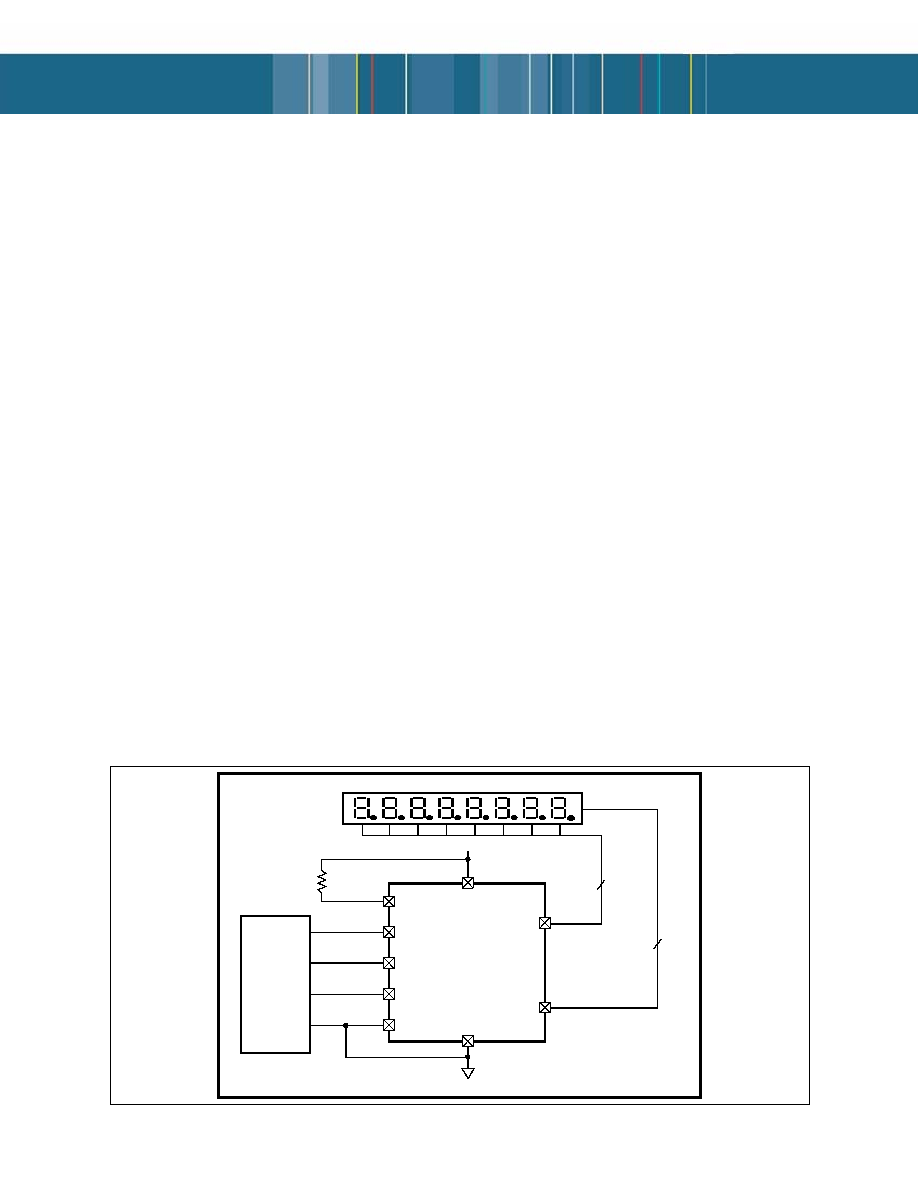
Figure 1. Typical Application Diagram
2 Key Features
!
10MHz SPI-, QSPI-, Microwire-Compatible
Serial I/O
!
Individual LED Segment Control
!
Segment Blinking Control (can be synchronized
across multiple drivers)
!
Hexadecimal- or BCD-Code/No-Decode Digit
Selection
!
3µA Low-Power Shutdown Current (typ; data
retained)
!
Extremely Low Operating Current 0.5mA in Open-
Loop
!
Digital and Analog Brightness Control
!
Display Blanked on Power-Up
!
Drive Common-Cathode LED Displays
!
Low-EMI Low Slew-Rate Limited Segment
Drivers (AS1107)
!
Supply Voltage Range: 2.7 to 5.5V
!
Software Reset
!
Optional External Clock
!
Packages:
- 24-pin DIP
- 24-pin SOIC
3 Applications
The AS1106 and AS1107 are ideal for bar-graph dis-
plays, instrument-panel meters, LED matrix displays, dot
matrix displays, set-top boxes, white goods, professional
audio equipment, medical equipment, industrial control-
lers and panel meters.
AS1106/
AS1107
8-Digit Microprocessor Display
DIG0 to
DIG7
SEG A to G
SEP DP
8 Digits
8 Segments
I/O
I/O
SCK
V
DD
I
SET
DIN
CLK
GND
GND
LOAD/CSN
+5V
9.53k
Micro-
processor

www.austriamicrosystems.com
Revision 2.2
2 - 20
AS1106, AS1107
austria
micro
systems
Data Sheet
4 Absolute Maximum Ratings
Stresses beyond those listed in Table 1 may cause permanent damage to the device. These are stress ratings only,
and functional operation of the device at these or any other conditions beyond those indicated in Section 5 Electrical
Characteristics on page 3 is not implied. Exposure to absolute maximum rating conditions for extended periods may
affect device reliability.
Table 1. Absolute Maximum Ratings
Parameter
Min
Max
Units
Notes
Voltage (with respect to GND)
V
DD
-0.3
7
V
DIN, CLK, LOAD/CSN
-0.3
7
V
All other pins
-0.3
7 or
V
DD
+ 0.3
V
Current
DIG 0:DIG 7 Sink Current
500
mA
SEG A:SEG G, SEG DP
100
mA
Continuous Power Dissipation
(T
AMB
= +85∫C)
Narrow plastic DIP
1066
mW
Derate 13.3mW/∫C
above +70∫C
Wide SOIC
941
mW
Derate 11.8mW/∫C
above +70∫C
Operating Temperature
Ranges (T
MIN
toT
MAX
)
AS1106PL, AS1106WL
0
+70
∫C
AS1106PE, AS1106WE
-40
+85
∫C
AS1107PL, AS1107WL
0
+70
∫C
Storage Temperature Range
-65
+150
∫C
Package Body Temperature (Wide SOIC)
1
1. The reflow peak soldering temperature (body temperature) is specified according to IPC/JEDEC J-STD-020C
"Moisture/Reflow Sensitivity Classification for non-hermetic Solid State Surface Mount Devices".
+260
∫C
Soldering Temperature (Narrow DIP)
2
2. Specified according JESD22-B106 "Resistance to Soldering Temperature for Through-Hole Mounted Devices".
+260
∫C
Humidity
5
85
%
Non-condensing
Electrostatic Discharge
3
3. Norm: MIL 883 E method 3015.
Digital outputs
1000
V
All other pins
1000
V
Latch-Up Immunity
4
4. Norm: JEDEC 17.
±200
mA
All pins except AS1106
pin 14: ±180 mA

www.austriamicrosystems.com
Revision 2.2
3 - 20
AS1106, AS1107
austria
micro
systems
Data Sheet
5 Electrical Characteristics
Conditions: V
DD
= 2.7 to 5.5V, R
SET
= 9.53k
±1%, T
AMB
= T
MIN
to T
MAX
(unless otherwise specified).
Table 2. Electrical Characteristics
Parameter
Symbol
Conditions
Min
Typ
Max
Unit
Operating Supply Voltage
V
DD
2.7
5.0
5.5
V
Shutdown Supply Current
I
DDSD
All digital inputs at V
DD
or
GND, T
AMB
= +25∫C
10
µA
Operating Supply Current
I
DD
R
SET
= open circuit.
1
mA
All segments and decimal
point on; I
SEG
= -40mA.
330
Display Scan Rate
f
OSC
8 digits scanned
500
800
1300
Hz
Digit Drive Sink Current
I
DIGIT
V
OUT
= 0.65V
320
mA
Segment Drive Source Current
I
SEG
V
DD
= 5.0V, V
OUT
= (V
DD
-1V)
-30
-40
-45
mA
Segment Current Slew Rate
(AS1107 only)
I
SEG
/
t
T
AMB
= +25∫C, V
DD
= 5.0V,
V
OUT
= (V
DD
-1V)
10
20
50
mA/µs
Segment Drive Current Matching
I
SEG
3.0
%
Digit Drive Leakage
(AS1107 only)
I
DIGIT
Digit off, V
DIGIT
= V
DD
-10
µA
Segment Drive Leakage
(AS1107 only)
I
SEG
Segment off, V
SEG
= 0V
1
µA
Digit Drive Source Current
(AS1106 only)
I
DIGIT
Digit off, V
DIGIT
= (V
DD
- 0.3V)
-2
mA
Segment Drive Sink Current
(AS1106 only)
I
SEG
Segment off, V
SEG
= 0.3V
5
mA
Slow Segment Blink Period (ON
phase, Internal Oscillator)
t
SLOWBLINK
0.64
1
1.65
s
Fast Segment Blink Period
(ON phase, Internal Oscillator)
t
FASTBLINK
0.32
0.5
0.83
s
Fast or Slow Segment Blink Duty
Cycle (Guaranteed by design)
49.9
50
50.1
%
Table 3. Logic Inputs/Outputs Characteristics
Parameter
Symbol
Conditions
Min
Typ
Max
Unit
Input Current DIN, CLK, LOAD/CSN
I
IH
, I
IL
V
IN
= 0V or V
DD
-1
1
µA
Logic High Input Voltage
V
IH
0.7 x V
DD
V
Logic Low Input Voltage
V
IL
V
DD
= 5.0V ± 10%
0.8
V
V
DD
= 3.0V ± 10%
0.6
Output High Voltage
V
OH
DOUT, I
SOURCE
= -1mA,
V
DD
= 5.0V ± 10%
V
DD
- 1
V
DOUT, I
SOURCE
= -1mA,
V
DD
= 3.0V ± 10%
V
DD
- 0.5
Output Low Voltage
V
OL
DOUT, I
SINK
= 1.6mA
0.4
V
Hysteresis Voltage
V
I
DIN, CLK, LOAD/CSN
1 V

www.austriamicrosystems.com
Revision 2.2
4 - 20
AS1106, AS1107
austria
micro
systems
Data Sheet
Note: See Figure 11 on page 7 for more information.
Table 4. Timing Characteristics
Parameter
Symbol
Conditions
Min
Typ
Max
Unit
CLK Clock Period
t
CP
100
ns
CLK Pulse Width High
t
CH
50
ns
CLK Pulse Width Low
t
CL
50
ns
CSM Fall to CLK Rise Setup Time
(AS1107 or AS1106 SPI-programmed)
t
CSS
25
ns
CLK Rise to LOAD/CSN Rise
Hold Time
t
CSH
0
ns
DIN Setup Time
t
DS
25
ns
DIN Hold Time
t
DH
0
ns
Output Data Propagation Delay
t
DO
C
LOAD
= 50pF
25
ns
LOAD Rising Edge to Next Clock Rising
Edge (AS1106 only)
t
LDCK
50
ns
Minimum LOAD/CSN Pulse High
t
CSW
50
ns
Data-to-Segment Delay
t
DSPD
2.25
ms
www.austriamicrosystems.com
Revision 2.2
5 - 20
AS1106, AS1107
austria
micro
systems
Data Sheet
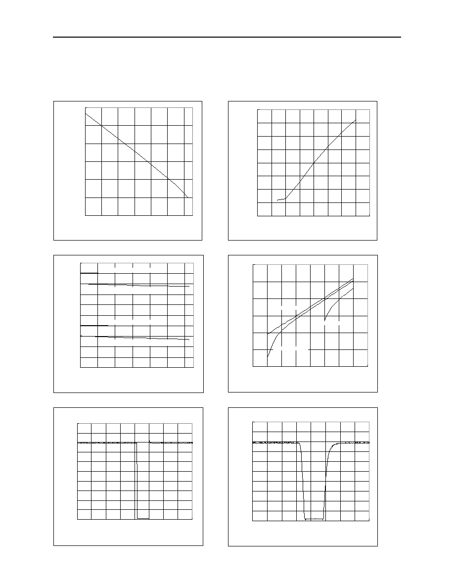
6 Typical Operating Characteristics
V
DD
= 5V, R
SET
= 9.53k
, T
AMB
= 25∫C (unless otherwise specified).
Figure 2. Scan Frequency vs.Temperature
Figure 3. Scan Frequency vs. V
DD
Figure 4. I
SEG
vs. Temperature
Figure 5. I
SEG
vs. V
DD
Figure 6. AS1106 Segment Output Current
Figure 7. AS1107 Segment Output Current
900
910
920
930
940
950
960
970
980
2
3
4
5
6
V
DD
(V)
F
OSC
(Hz)
930
940
950
960
970
980
990
-40
-20
0
20
40
60
80
T
AMB
[∞C]
F
OSC
(Hz)
0
5
10
15
20
25
30
35
40
45
50
-40
-20
0
20
40
60
80
T
AMB
(∞C)
I
SEG
(mA)
0
10
20
30
40
50
60
2
2.5
3
3.5
4
4.5
5
5.5
6
V
DD
(V)
I
SEG
(mA)
V
DD
= 5V, V
OUT
= 2.4V
V
DD
= 5V, V
OUT
= 4V
V
DD
= 2.7V, V
OUT
= 2V
V
DD
= 2.7V, V
OUT
= 2.4V
V
OUT
= 1.7V
V
OUT
= 2.4V
V
OUT
= 4V
Intensity = 31/32 (0Fh)
0
5
10
15
20
25
30
35
40
45
50
0.0 5.0 10.0 15.0 20.0 25.0 30.0 35.0 40.0
Time (µs)
I
SEG
(mA)
Intensity = 15/16 (0Fh)
0
5
10
15
20
25
30
35
40
45
50
0.0
5.0 10.0 15.0 20.0 25.0 30.0 35.0 40.0
Time (µs)
I
SEG
(mA)