 | –≠–ª–µ–∫—Ç—Ä–æ–Ω–Ω—ã–π –∫–æ–º–ø–æ–Ω–µ–Ω—Ç: AS1500-Z | –°–∫–∞—á–∞—Ç—å:  PDF PDF  ZIP ZIP |
Data Sheet AS1500/1/2/3
Revision 1.0, Oct 2004
Page 1 of 8
Key Features
-
256-Position
-
Available in four Resistance values
-
AS1500 resistance 10kOhms
-
AS1501 resistance 20kOhms
-
AS1502 resistance 50kOhms
-
AS1503 resistance 100kOhms
-
Power Shutdown --Less than 1 µA
-
3-Wire SPI-Compatible Serial Data Input
-
10 MHz Update Data Loading Rate
-
2.7 V to 5.5 V Single-Supply Operation
-
Temperature Range ≠40∞C to +125∞C
-
Package SO-8
-
Compatible to AD8400
General Description
The AS1500 is a digital potentiometer with 256
programmable steps. The values of the resistor can be
controlled via 3 wire serial interface capable to handle
programming rates up to 10MHz. The AS1500 is available in
four different resistor values. The AS1500 incorporates a
10k
, the AS1501 a 20k, the AS1502 a 50k and the
AS1503 a 100k
fixed resistor. The wiper contact taps the
fixed resistor at points determined by the 8-bit digital code
word. The resistance between the wiper and the endpoint of
the resistor is linear. The switching action is performed in a
way that no glitches occur. Furthermore the AS150x product
family includes a shutdown mode, where it consumes less
than 1µA. The AS150x is available in an 8-pin SOIC
package. All parts are guaranteed to operate over the
extended industrial temperature range of ≠40∞C to +125∞C.
Applications
-
Line Impedance Matching
-
Volume Control, Panning
-
Mechanical Potentiometer Replacement
-
Power Supply Adjustment
-
Programmable Filters, Delays, Time Constants
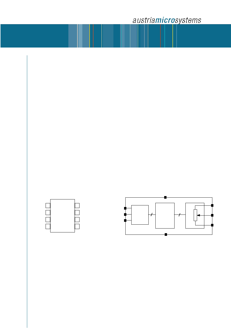
Figure 1
Pinout andfunctional Block Diagram of Digital Potentiometer AS150x family
PRELIMINARY FACT SHEET
Digital Potentiometer
AS1500/AS1501/AS1502/AS1503
DATASHEET
8-Bit
Latch
10 Bit
Serial
Latch
8
8
SDI
CK
CSN
A
W
B
VDD
GND
AS1500
W
VDD
GND
CSN
7
6
2
3
AS150x
Top View
CK
A
B
SDI
1
4
8
5

Data Sheet AS1500/1/2/3
Revision 1.0, Oct 2004
Page 2 of 8
ABSOLUTE MAXIMUM RATINGS
(TA = 25∞C, unless otherwise noted.)
Parameter
Limits
VDD to GND
≠0.3V, +7V
VA, VB, VW to GND
0V, VDD
AX ≠ BX, AX ≠ WX, BX ≠ WX
±20mA
Digital Input and Output Voltage to GND
0V, +7V
Operating Temperature Range
≠40∞C to +125∞C
Maximum Junction Temperature (TJ max)
150∞C
Storage Temperature
≠65∞C to +150∞C
Package body temperature
1
260∞C
Package Power Dissipation
(TJ max ≠ TA) /
JA
ESD
2
1kV
Table 1: Absolute Maximum Ratings
Pin
Name
Description
1
B
Terminal B RDAC
2
GND
Ground
3
CSN
Chip Select Input, Active Low. When CS returns high,
data in the serial input register is loaded into the DAC
register.
4
SDI
Serial Data Input
5
CK
Serial Clock Input, Positive Edge Triggered.
6
VDD
Positive power supply, specified for operation at both 3V
and 5V.
7
W
Wiper RDAC
8
A
Terminal A RDAC
Table 2: Pin Function Description
1
The reflow peak soldering temperature (body temperature) is specified according IPC/JEDEC J-STD-020C "Moisture/Reflow Sensitivity
Classification for non hermetic Solid State Surface Mount Devices".
2
HBM MIL-Std883E 3015.7methods.

Data Sheet AS1500/1/2/3
Revision 1.0, Oct 2004
Page 3 of 8
AS1500 / AS1501 ≠ SPECIFICATIONS
VDD = 3V±10% or 5V±10%, V
A
= VDD, V
B
= 0V, ≠40∞C
T
A
+125∞C unless otherwise noted.
ELECTRICAL CHARACTERISTICS ≠ 10k and 20k VERSIONS
Parameter
Symbol
Conditions
Min
Typ
3
Max
Unit
DC CHARACTERISTICS RHEOSTAT MODE
T
A
= 25∞C, VDD = 5V, AS1500, Version: 10k
8
10
12
k
Nominal Resistance
4
R
AB
T
A
= 25∞C, VDD = 5V, AS1501, Version: 20k
16
20
24
k
Resistance Tempco
5
R
AB
/
T V
AB
= VDD, Wiper = No Connect
500
ppm/∞C
Wiper Resistance
R
W
VDD = 5V
20
100
200
Resistor Differential NL
6
R-DNL
R
WB
, VDD = 5V, V
A
= No Connect
≠1
±1/4
+1
LSB
Resistor Integral NL
R-INL
R
WB
, VDD = 5V, V
A
= No Connect
≠2
±1/2
+2
LSB
DC CHARACTERISTICS POTENTIOMETER DIVIDER
Resolution
N
8
Bits
VDD = 5.5V T
A
= 25∞C
≠2
±1/2
+2
LSB
Integral Nonlinearity
INL
VDD = 2.7V T
A
= 25∞C
≠2
±1/2
+2
LSB
VDD = 5.5V T
A
= 25∞C
≠1
±1/4
+1
LSB
Differential Nonlinearity
DNL
VDD = 2.7V T
A
= 25∞C
≠1
±1/4
+1
LSB
Voltage Divider Tempco
V
W
/
T Code = 80
H
15
ppm/∞C
Full-Scale Error
V
WFSE
Code = FF
H
, VDD = 5.5V
≠4
≠2.8
0
LSB
Zero-Scale Error
V
WZSE
Code = 00
H
, VDD = 5.5V
0
1.3
2
LSB
RESISTOR TERMINALS
Voltage Range
7
V
A, B, W
0
VDD
V
Capacitance
8
Ax, Bx
C
A, B
f =1MHz, Measured to GND, Code = 80
H
75
pF
Capacitance Wx
C
W
f =1MHz, Measured to GND, Code = 80
H
120
pF
DIGITAL INPUTS AND OUTPUTS
Input Logic High
V
IH
VDD = 5V
2.4
V
Input Logic Low
V
IL
VDD = 5V
0.8
V
Input Logic High
V
IH
VDD = 3V
2.1
V
Input Logic Low
V
IL
VDD = 3V
0.6
V
Input Current
I
IH
, I
IL
V
IN
= 5V or 0V, VDD = 5V
±1
µA
Input Capacitance
C
IL
5
pF
POWER SUPPLIES
Power Supply Range
VDD
2.7
5.5
V
Supply Current (CMOS)
IDD
V
IH
= VDD or V
IL
= 0V, VDD = 5.5V
0.1
1
µA
Supply Current (TTL)
9
IDD
V
IH
= 2.4V or 0.8V, VDD = 5.5V
0.9
4
mA
Power Dissipation
(CMOS)
10
P
DISS
V
IH
= VDD or V
IL
= 0V, VDD = 5.5V
27.5
µW
AS1500, Version: 10k
-54
-25
dB
Power Supply Suppression
Ratio
PSSR
VDD = 5V + 0.5V
P
sine wave @ 1kHz
AS1501, Version: 20k
-52
-25
dB
DYNAMIC CHARACTERISTICS
11
BW_10k R
WB
= 10k
, VDD = 5V
1000
kHz
Bandwidth ≠3dB
Bandwidth ≠3dB
BW_20k R
WB
= 20k
, VDD = 5V
500
kHz
Total Harmonic Distortion
THD
W
V
A
= 1V
RMS
+ 2V
DC
, V
B
= 2V
DC
, f = 1kHz
0.003
%
t
S
_10k
R
WB
= 5k
, V
A
= VDD, V
B
= 0V, ±1% Error
Band
2
µs
V
W
Settling Time
t
S
_20k
R
WB
= 10k
, V
A
= VDD, V
B
= 0V, ±1% Error
Band
4
µs
e
NWB
_10k R
WB
= 5k
, f =1kHz
9
nV/
Hz
Resistor Noise Voltage
e
NWB
_20k R
WB
= 10k
, f =1kHz
13
nV/
Hz
Table 3: Electrical Characteristics ≠ 10k and 20k Versions
3
Typicals represent average readings at 25∞C and VDD = 5V.
4
Wiper is not connected. I
AB
= 350µA for the 10k
version and 175µA for the 20k version.
5
All Tempcos are guaranteed by design and not subject to production test.
6
Terminal A is not connected. I
W
= 350µA for the 10k
version and 175µA for the 20k version.
7
Resistor terminals A, B, W have no limitations on polarity with respect to each other.
8
All capacitances are guaranteed by design and not subject to production test. Resistor-terminal capacitance tests are measured with 2.5V
bias on the measured terminal. The remaining resistor terminals are left open circuit.
9
Worst-case supply current consumed when input logic level at 2.4V, standard characteristic of CMOS logic.
10
P
DISS
is calculated from (IDD◊VDD). CMOS logic level inputs result in minimum power dissipation.
11
All dynamic characteristics are guaranteed by design and not subject to production test. All dynamic characteristics use VDD=5V.

Data Sheet AS1500/1/2/3
Revision 1.0, Oct 2004
Page 4 of 8
AS1502 / AS1503 ≠ SPECIFICATIONS
VDD = 3V±10% or 5V±10%, V
A
= VDD, V
B
= 0V, ≠40∞C
T
A
+125∞C unless otherwise noted.
ELECTRICAL CHARACTERISTICS ≠ 50k and 100k VERSIONS
Parameter
Symbol
Conditions
Min
Typ
12
Max
Unit
DC CHARACTERISTICS RHEOSTAT MODE
T
A
= 25∞C, VDD = 5V, AS1502, Version: 50k
40
50
60
k
Nominal Resistance
13
R
AB
T
A
= 25∞C, VDD = 5V, AS1503, Version: 100k
80
100
120
k
Resistance Tempco
14
R
AB
/
T V
AB
= VDD, Wiper = No Connect
500
ppm/∞C
Wiper Resistance
R
W
VDD = 5V
20
100
200
Resistor Differential NL
15
R-DNL
R
WB
, VDD = 5V, V
A
= No Connect
≠1
±1/4
+1
LSB
Resistor Integral NL
R-INL
R
WB
, VDD = 5V, V
A
= No Connect
≠2
±1/2
+2
LSB
DC CHARACTERISTICS POTENTIOMETER DIVIDER
Resolution
N
8
Bits
VDD = 5.5V T
A
= 25∞C
≠4
±1
+4
LSB
Integral Nonlinearity
INL
VDD = 2.7V T
A
= 25∞C
≠4
±1
+4
LSB
VDD = 5.5V T
A
= 25∞C
≠1
±1/4
+1
LSB
Differential Nonlinearity
DNL
VDD = 2.7V T
A
= 25∞C
≠1
±1/4
+1
LSB
Voltage Divider Tempco
V
W
/
T Code = 80
H
15
ppm/∞C
Full-Scale Error
V
WFSE
Code = FF
H
, VDD = 5.5V
≠1
≠0.25
0
LSB
Zero-Scale Error
V
WZSE
Code = 00
H
, VDD = 5.5V
0
0.1
1
LSB
RESISTOR TERMINALS
Voltage Range
16
V
A, B, W
0
VDD
V
Capacitance
17
Ax, Bx
C
A, B
f = 1MHz, Measured to GND, Code = 80
H
15
pF
Capacitance Wx
C
W
f = 1MHz, Measured to GND, Code = 80
H
80
pF
DIGITAL INPUTS AND OUTPUTS
Input Logic High
V
IH
VDD = 5V
2.4
V
Input Logic Low
V
IL
VDD = 5V
0.8
V
Input Logic High
V
IH
VDD = 3V
2.1
V
Input Logic Low
V
IL
VDD = 3V
0.6
V
Input Current
I
IH
, I
IL
V
IN
= 5V or 0V, VDD = 5V
±1
µA
Input Capacitance
C
IL
5
pF
POWER SUPPLIES
Power Supply Range
VDD
2.7
5.5
V
Supply Current (CMOS)
IDD
V
IH
= VDD or V
IL
= 0V, VDD = 5.5V
0.1
1
µA
Supply Current (TTL)
18
IDD
V
IH
= 2.4V or 0.8V, VDD = 5.5V
0.9
4
mA
Power Dissipation
(CMOS)
19
P
DISS
V
IH
= VDD or V
IL
= 0V, VDD = 5.5V
27.5
µW
AS1502, Version: 50k
-43
tbd.
dB
Power Supply Suppression
Ratio
PSSR
VDD = 5V + 0.5V
P
sine wave @ 1kHz
AS1503, Version:
100k
-48
tbd.
dB
DYNAMIC CHARACTERISTICS
20
BW_50k R
WB
= 50k
, VDD = 5V
220
kHz
Bandwidth ≠3dB
Bandwidth ≠3dB
BW_100k R
WB
= 100k
, VDD = 5V
110
kHz
Total Harmonic Distortion
THD
W
V
A
= 1V
RMS
+ 2V
DC
, V
B
= 2V
DC
, f = 1kHz
0.003
%
t
S
_50k
R
WB
= 50k
, V
A
= VDD, V
B
= 0V, ±1% Error
Band
9
µs
V
W
Settling Time
t
S
_100k R
WB
= 100k
, V
A
= VDD, V
B
= 0V, ±1% Error
Band
18
µs
e
NWB
_50k R
WB
= 50k
, f = 1kHz
20
nV/
Hz
Resistor Noise Voltage
e
NWB
_100
k
R
WB
= 100k
, f = 1kHz
29
nV/
Hz
Table 4: Electrical Characteristics ≠ 50k and 100k Versions
12
Typicals represent average readings at 25∞C and VDD = 5V.
13
Wiper is not connected. I
AB
= 70µA for the 50k
version and 35µA for the 100k version.
14
All Tempcos are guaranteed by design and not subject to production test.
15
Terminal A is not connected. I
W
= 70µA for the 50k
version and 35µA for the 100k version.
16
Resistor terminals A, B, W have no limitations on polarity with respect to each other.
17
All capacitances are guaranteed by design and not subject to production test. Resistor-terminal capacitance tests are measured with 2.5V
bias on the measured terminal. The remaining resistor terminals are left open circuit.
18
Worst-case supply current consumed when input logic level at 2.4V, standard characteristic of CMOS logic.
19
P
DISS
is calculated from (IDD◊VDD). CMOS logic level inputs result in minimum power dissipation.
20
All dynamic characteristics are guaranteed by design and not subject to production test. All dynamic characteristics use VDD=5V.

Data Sheet AS1500/1/2/3
Revision 1.0, Oct 2004
Page 5 of 8
AS150x ≠ SPECIFICATIONS
(VDD = 3V±10% or 5V±10%, VA = VDD, VB = 0V,
≠40∞C
TA+125∞C unless otherwise noted.)
ELECTRICAL CHARACTERISTICS≠ALL
VERSIONS
Parameter
Sym-
bol
Conditions Min
Typ
21
Max Unit
SWITCHING CHARACTERISTICS
22, 23
Input Clock
Pulsewidth
t
CH
, t
CL
Clock Level
High or Low
50
ns
Data Setup Time
t
DS
5
ns
Data Hold Time
t
DH
5
ns
CSN Setup Time
t
CSS
10
ns
CSN High
Pulsewidth
t
CSW
10
ns
CK Fall to CSN Rise
Hold Time
t
CSH
0
ns
CSN Rise to Clock
Rise Setup
t
CS1
10
ns
Table 5: Switching Characteristics
Detailed Description
Serial-Programming
Programming of the AS150x is done via the 3 wire serial
interface. The three input signals are serial data input
(SDI), clock(CK) and chip select (CS). A programming
sequence consists of 10-bit, where the last eight bit
contain the code word for the resistor value. The first two
bits A1 and A0 have to be low(see Table ). The data is
shifted into the internal 10 Bit register with the rising edge
of the CK signal. With the rising edge of the CSN signal
the data becomes valid and the resistance is updated (see
figure 2). A detailed block diagram is shown in figure 3.
A1 A0
D7
D6
D5
D4
D3
D2
D1
D0
0
0 MSB Data LSB
Table 6: Serial data format (16 bits)
21
Typicals represent average readings at 25∞C and VDD=5V.
22
Guaranteed by design and not subject to production test.
Resistor-terminal capacitance tests are measured with 2.5V
bias on the measured terminal. The remaining resistor
terminals are left open circuit.
23
See timing diagram for location of measured values. All input
control voltages are specified with t
R
= t
F
= 1ns (10% to 90% of
VDD) and timed from a voltage level of 1.6V. Switching
characteristics are measured using VDD=3V or 5V. To avoid
false clocking, a minimum input logic slew rate of 1V/µs should
be maintained.
Figure 2: Timing Diagram
Figure 3: Detailed Timing Diagram
Rheostat Operation
The digital potentiometer family AS150x offers nominal
resistor values of 10k
, 20 k, 50k and 100k. The
resistor has 256 contact points where the wiper can access
the resistor. The 8-bit code word determines the position
of the wiper and is decoded through an internal logic. The
lowest code 00h is related to the terminal B. The
resistance is then only determined by the wiper resistance
(100
). The resistance for the next code 01h is the
nominal resistor RAB (10k
, 20 k, 50k or 100k)
divided through 256 plus the wiper resistor. In case of
AS1501 (10k
) the total resistance is 39+100=139.
Accordingly the resistor for code 02h is 78
+100=178.
The last code 255h does not connect to terminal A directly
(see Figure 5). So the maximum value is 10000
- 39
+100
= 10061. The general formula for the calculation
of the resistance R
WB
is:
R
WB
(Dx)= (Dx)/256
R
AB
+ R
W
where R
AB
is the nominal resistance between terminal A
and B, R
W
is the wiper resistance and D
X
is the 8-Bit Code
word. In Table 7 the resistor values between the wiper and
terminal B for AS1501 are given for specific codes D
X
. In
the zero-scale condition the wiper resistance of 100
remains present.
1
1
1
0
0
0
0V
V
OUT
CS
CK
SD
VD
DAC Register
A1 A0 D7 D6 D5 D4 D3 D2 D1 D0
SDI
V
OUT
CK
CSN
V
DD
0
0
0
0V
1
1
1
±1% Error
±1%
A
X
or
A
X
or
t
D
t
D
t
C
t
CS
t
CS
t
CS
t
CS
t
S
t
CL

Data Sheet AS1500/1/2/3
Revision 1.0, Oct 2004
Page 6 of 8
D
X
(Dec)
R
WB
(
)
Output State
255
10061
Full Scale
128
5100
Midscale
1
139
1 LSB
0
100
Zero-Scale
(Wiper Contact Resistance)
Table 7: RDAC-Codes WB
The maximum current through the wiper and terminal B is
5mA. If the current exceeds this limit the internal switches
can degrade or even be damaged. As a mechanical
potentiometer the resistance R
WA
and R
WB
are totally
symmetrical. The relation between them is shown in Figure
4.
Figure 4: R
WA
and R
WB
versa Code
The resistance RWA is the complimentary resistor to RWB
and can be controlled digitally as well. RWA starts at the
maximum value of the nominal resistance and is reduced
with increasing 8-Bit code words. The formula to calculate
RWA is given below:
R
WA
(Dx)= (256 - Dx)/256
R
AB
+ R
W
where R
AB
is the nominal resistance between terminal A
and B, R
W
is the wiper resistance and D
X
is the 8-Bit Code
word. In Table 8 the resistor values between the wiper and
terminal B for AS1501 are given for specific codes D
X
.
D
X
(Dec)
R
WA
(
)
Output State
255
89
Full Scale
128
5050
Midscale
1
10011
1 LSB
0
10050
Zero-Scale
Table 8: RDAC-Codes WA
Figure 5: Equivalent RDAC Circuit
Voltage Output Operation
The AS150x family can easily used in an voltage output
mode, where the output voltage is proportional to an
applied voltage to a given terminal. When 5V are applied to
terminal A and B is set to ground the ouput voltage at the
wiper starts at zero volts up to 1LSB less then 5V. One
LSB of voltage corresponds to the voltage applied at
terminal AB divided through 256 steps of possible wiper
settings. The formula is given by
V
W
(Dx)= (Dx)/256
V
AB
+ V
B
where V
AB
is the voltage applied between terminal A and B,
V
W
is the voltage at the wiper, D
X
is the 8-Bit Code word
and V
B
is the voltage at terminal B. The temperature drift is
significant better than in Rheostat mode, since the
temperature coefficient is determined by the internal
resistor ratio. Therefore the temperature drift is only
15ppm/∞C.
Applications
The digital potentiometer can replace in many applications
the analog trimming potentiometer. The digital
potentiometer is not sensitive to vibrations and shocks. It
has an extremely small form-factor and can be adjusted
very fast (e.g. AS1500 has an update rate of 600kHz)
Furthermore the temperature drift, resolution and noise are
significant better and cannot be achieved with a
mechanical trimming potentiometer. Due to the
programmability the resistor settings can be stored in the
system memory, so that after a power down the exact
settings can be recalled easily.
All analog signals must remain within 0 to VDD range. For
standard potentiometer applications the wiper output can
be used directly. In the case of a low impedance load a
buffer shall be used.
CODE -
R
WA
(
D
),
R
WB
(
D
)
- % of
R
W
R
W
0
25
50
75
10
0
64
12
19
25
RDAC
LATCH
AND
DECODE
R
S
=R
NOMINAL
/ 256
R
S
R
S
R
S
R
S
A
W
B
D7
D6
D5
D4
D3
D2
D1
D0

Data Sheet AS1500/1/2/3
Revision 1.0, Oct 2004
Page 7 of 8
Package Information
The AS150x family is offered in a 8-pin SOIC package:

Data Sheet AS1500/1/2/3
Revision 1.0, Oct 2004
Page 8 of 8
Package Dimensions in Inch and mm (values for N = 8 Pin package are valid):
Ordering Information
Part
Resistor Pin Package Delivery Form
AS1500
10k
8-pin SOIC
Tubes
AS1501
20k
8-pin SOIC
Tubes
AS1502
50k
8-pin SOIC
Tubes
AS1503
100k
8-pin SOIC
Tubes
AS1500-T
10k
8-pin SOIC
T&R
AS1501-T
20k
8-pin SOIC
T&R
AS1502-T
50k
8-pin SOIC
T&R
AS1503-T
100k
8-pin SOIC
T&R
For Pb-free package use suffix `-Z`
Copyright
Copyright © 2004 austriamicrosystems. Trademarks
registered Æ. All rights reserved. The material herein may
not be reproduced, adapted, merged, translated, stored, or
used without the prior written consent of the copyright
owner. To the best of its knowledge, austriamicrosystems
asserts that the information contained in this publication is
accurate and correct.
Contact
austriamicrosystems AG
A 8141 Schloss Premst‰tten, Austria
T. +43 (0) 3136 500 0
F. +43 (0) 3136 525 01
info@austriamicrosystems.com