 | –≠–ª–µ–∫—Ç—Ä–æ–Ω–Ω—ã–π –∫–æ–º–ø–æ–Ω–µ–Ω—Ç: AS1703-T | –°–∫–∞—á–∞—Ç—å:  PDF PDF  ZIP ZIP |

AS1702, AS1703, AS1704, AS1705
1.6W Single-Channel Audio Power Amplifiers
austria
micro
systems
D a ta S h e e t
www.austriamicrosystems.com
Revision 1.01
1 - 13
1 General Description
The AS1702, AS1703, AS1704, and AS1705 are single-
channel differential audio power-amplifiers designed to
drive 4 and 8
loads. The integrated gain circuitry of
these amplifiers and their small size make them ideal for
2.7- to 5V-powered portable audio devices.
The differential input design improves noise rejection
and provides common-mode rejection. A bridge-tied
load (BTL) design minimizes external component count,
while providing Hi-Fi audio power amplification.
The devices deliver 1.6W continuous average power per
channel to a 4
load with less than 1% total harmonic
distortion (plus noise), while operating from a single 2.7
to 5V supply.
In order to facilitate reduced component designs, the
devices are available with different gain levels:
!
AS1702 ≠ Adjustable Gain (via external components)
!
AS1703 ≠ A
V
= 0dB
!
AS1704 ≠ A
V
= 3dB
!
AS1705 ≠ A
V
= 6dB
Integrated shutdown circuitry disables the bias genera-
tor and amplifiers, and reduces quiescent current con-
sumption to less than 100nA. The shutdown input can
be set as active-high or active-low. All devices contain
comprehensive click-and-pop suppression circuitry that
reduces audible clicks and pops during power-up and
shutdown.
The AS1702, AS1703, AS1704, and AS1705 are pin
compatible with the LM4895 and the MAX9718A/B/C/D.
The devices are available in a 10-pin MSOP package.
Figure 1. Simplified Block Diagram
2 Key Features
!
2.7 to 5.5V (V
CC
) Single-Supply Operation
!
THD+N: 1.6W into 4
at 1% (per Channel)
!
Differential Input
!
Adjustable Gain Option (AS1702)
!
Internal Fixed Gain to Reduce External Component
Count (AS1703, AS1704, AS1705)
!
<100nA Low-Power Shutdown Mode
!
Click and Pop Suppression
!
Pin-Compatible National Semiconductor LM4895
(AS1705) and Maxim MAX9718A/B/C/D
!
Operating Temperature Range: -40 to +85∞C
!
Low-Cost MSOP-10 Package
3 Applications
The devices are ideal as audio front-ends for battery
powered audio devices such as MP3 and CD players,
mobile phones, PDAs, portable DVD players, and any
other hand-held battery-powered device.
AS1702, AS1703,
AS1704, AS1705
OUT+
Single Supply
2.7 to 5.5V
SHDN
IN+
IN-
OUT-
SHDM
R
L =
4 or 8
+
≠
GND

www.austriamicrosystems.com
Revision 1.01
2 - 13
AS1702, AS1703, AS1704, AS1705
austria
micro
systems
Data Sheet
4 Absolute Maximum Ratings
Stresses beyond those listed in Table 1 may cause permanent damage to the device. These are stress ratings only,
and functional operation of the device at these or any other conditions beyond those indicated in Section 5 Electrical
Characteristics on page 3 is not implied. Exposure to absolute maximum rating conditions for extended periods may
affect device reliability.
Table 1. Absolute Maximum Ratings
Parameter
Min
Max
Unit
Comments
Supply Voltage (V
CC
to GND)
-0.3
+7
V
Any Other Pin to GND
-0.3
V
CC
+ 0.3
V
Input Current (Latchup Immunity)
-100
100
mA
JEDEC 17
Continuous Power Dissipation
(T
AMB
= +70∞C)
TBD
mW
MSOP-10 (Derate 10.3mW/∞C
above +70∞C)
Electro-Static Discharge (ESD)
1
kV
Human Body Model and MIL-
Std883E 3015.7methods
Operating Temperature Range (T
AMB
)
-40
+85
∞C
Storage Temperature Range
-65
+150
∞C
Package Body Temperature
260
∞C

www.austriamicrosystems.com
Revision 1.01
3 - 13
AS1702, AS1703, AS1704, AS1705
austria
micro
systems
Data Sheet
5V Operation
5 Electrical Characteristics
5.1 5V Operation
V
CC
= 5V, GND = 0V, SHDN = V
CC
, SHDM = GND, R
IN
= R
F
= 10k
(AS1702), T
AMB
= +25∞C, C
BIAS
= 0.1µF, no load.
Typical values are at T
AMB
= +25∞C (unless otherwise specified). All specifications are 100% tested at T
AMB
= +25∞C
(unless otherwise specified). Specifications over temperature (T
AMB
= T
MIN
to T
MAX
) are guaranteed by design, not
production tested.
Table 2. Electrical Characteristics ≠ 5V Supply
Symbol
Parameter
Conditions
Min
Typ
Max
Unit
V
CC
Supply Voltage
2.7
5.5
V
I
CC
Supply Current
1
1. Quiescent power supply current is specified and tested with no load. Quiescent power supply current depends
on the offset voltage when a practical load is connected to the amplifier. Guaranteed by design.
V
IN-
= V
IN+
= V
BIAS
;
T
AMB
= -40 to +85∞C, per amplifier
8
10.4
mA
I
SHDN
Shutdown Supply
SHDN = SHDM = GND per amplifier
0.05
1
µA
V
IH
SHDN
,
SHDM
Threshold
0.7 x V
CC
V
V
IL
0.3 x V
CC
V
BIAS
Common-Mode Bias
Voltage
2
2. Common-mode bias voltage is the voltage on BIAS and is nominally V
CC
/2.
V
CC
/2 - 5% V
CC
/2 V
CC
/2 + 5%
V
V
OS
Output Offset Voltage
V
IN-
= V
IN+
= V
BIAS
A
V
= 0dB (AS1703)
±1
±10
mV
A
V
= 3dB (AS1704)
±1
±15
A
V
= 6dB (AS1705)
±1
±20
V
IC
Common-Mode Input
Voltage
Inferred from CMRR
Test
A
V
= 0dB (AS1703)
0.5
V
CC
- 0.5
V
A
V
= 3dB (AS1704)
0.5
V
CC
- 0.6
A
V
= 6dB (AS1705)
0.5
V
CC
- 0.8
External Gain AS1702
0.5
V
CC
- 1.2
R
IN
Input Impedance
AS1703, AS1704, AS1705
10
15
20
k
CMRR
Common-Mode
Rejection Ration
-50
-60
dB
f
N
= 1kHz
-64
PSRR
Power Supply
Rejection Ratio
V
IN-
= V
IN+
= V
BIAS
;
V
RIPPL
E = 200mVp-p;
R
L
= 8
;
C
BIAS
= 1µF
f = 217Hz
-79
dB
f = 1kHz
-73
P
OUT
Output Power
3
3. Output power is specified by a combination of a functional output current test and characterization analysis.
THD+N = 1%;
f
IN
= 1kHz
R
L
= 8
0.8
1.2
W
R
L
= 4
1.6
THD+N
Total Harmonic
Distortion plus Noise
4
4. Measurement bandwidth for THD+N is 22Hz to 22kHz.
R
L
= 4
, f
IN
= 1kHz, P
OUT
= 1.28W,
V
CC
= 5V, A
V
= 6dB
0.06
%
R
L
= 8
, f
IN
= 1kHz, P
OUT
= 0.9W,
V
CC
= 5V, A
V
= 6dB
0.03
Gain Accuracy
AS1703, AS1704, AS1705
±1
±2
%
Thermal Shutdown
Threshold
+145
∞C
Thermal Shutdown
Hysteresis
9
∞C
C
LOAD
Maximum Capacitive
Drive
Bridge-tied capacitance
500
pF
t
PU
Power-up/Enable from
Shutdown Time
125 ms
t
SHDN
Shutdown Time
3.5
µs
V
POP
Turn-Off Transient
5
5. Peak voltage measured at power-on, power-off, into or out of SHDN. Bandwidth defined by A-weighted filters,
inputs at AC GND. V
CC
rise and fall times
1ms.
50
mV

www.austriamicrosystems.com
Revision 1.01
4 - 13
AS1702, AS1703, AS1704, AS1705
austria
micro
systems
Data Sheet
3V Operation
5.2 3V Operation
V
CC
= 3V, GND = 0V, SHDN = V
CC
, SHDM = GND, R
IN
= R
F
= 10k
(AS1702), T
AMB
= +25∞C, C
BIAS
= 0.1µF, no load.
Typical values are at T
AMB
= +25∞C (unless otherwise specified.) All specifications are 100% tested at T
AMB
= +25∞C.
Specifications over temperature (T
AMB
= T
MIN
to T
MAX
) are guaranteed by design, not production tested.
Table 3. Electrical Characteristics ≠ 3V Supply
Symbol
Parameter
Conditions
Min
Typ
Max
Unit
I
CC
Supply Current
1
1. Quiescent power supply current is specified and tested with no load. Quiescent power supply current depends
on the offset voltage when a practical load is connected to the amplifier. Guaranteed by design.
V
IN-
= V
IN+
= V
BIAS
;
T
AMB
= -40 to +85∞C, per amplifier
7.5
mA
I
SHDN
Shutdown Supply
SHDN = SHDM = GND per amplifier
0.05
1
µA
V
IH
SHDN
,
SHDM
Threshold
0.7 x V
CC
V
V
IL
0.3 x V
CC
V
BIAS
Common-Mode
Bias Voltage
2
2. Common-mode bias voltage is the voltage on BIAS and is nominally V
CC
/2.
V
CC
/2 - 5% V
CC
/2 V
CC
/2 + 5%
V
V
OS
Output Offset
Voltage
V
IN-
= V
IN+
= V
BIAS
A
V
= 0dB (AS1703)
±1
±10
mV
A
V
= 3dB (AS1704)
±1
±15
A
V
= 6dB (AS1705)
±1
±20
V
IC
Common-Mode
Input Voltage
Inferred from CMRR
Test
A
V
= 0dB (AS1703)
0.5
V
CC
- 0.7
mV
A
V
= 3dB (AS1704)
0.5
V
CC
- 0.8
A
V
= 6dB (AS1705)
0.5
V
CC
- 1.0
External gain AS1702
0.5
V
CC
- 1.2
R
IN
Input Impedance
AS1703, AS1704, AS1705
10
15
20
k
CMRR
Common-Mode
Rejection Ration
-50
-60
dB
f
N
= 1kHz
-64
PSRR
Power Supply
Rejection Ratio
V
IN-
= V
IN+
= V
BIAS
;
V
RIPPLE
= 200mVp-p;
R
L
= 8
;
C
BIAS
= 1µF
f = 217Hz
-79
dB
f = 1kHz
-73
P
OUT
Output Power
3
3. Output power is specified by a combination of a functional output current test and characterization analysis.
R
L
= 4
,
THD+N = 1%; f
IN
= 1kHz
590
mW
R
L
= 8
,
THD+N = 1%; f
IN
= 1kHz
430
THD+N
Total Harmonic
Distortion plus
Noise
4
4. Measurement bandwidth for THD+N is 22Hz to 22kHz.
R
L
= 4
, f
IN
= 1kHz, P
OUT
= 460mW, A
V
= 6dB
0.06
%
R
L
= 8
, f
IN
= 1kHz, P
OUT
= 330mW, A
V
= 6dB
0.04
Gain Accuracy
AS1703, AS1704, AS1705
±1
±2
%
Thermal Shutdown
Threshold
+145
∞C
Thermal Shutdown
Hysteresis
9
∞C
C
LOAD
Maximum
Capacitive Drive
Bridge-tied capacitance
500
pF
t
PU
Power-up/Enable
from
Shutdown Time
125
ms
t
SHDN
Shutdown Time
3.5
µs
V
POP
Turn-Off Transient
5
5. Peak voltage measured at power-on, power-off, into or out of SHDN. Bandwidth defined by A-weighted filters,
inputs at AC GND. V
CC
rise and fall times
1ms.
50
mV

www.austriamicrosystems.com
Revision 1.01
5 - 13
AS1702, AS1703, AS1704, AS1705
austria
micro
systems
Data Sheet
Bias
6 Detailed Description
The AS1702, AS1703, AS1704, and AS1705 are 1.6W high output-current audio amplifiers (configured as BTL ampli-
fiers), and contain integrated low-power shutdown and click- and pop-suppression circuitry. Two inputs (SHDM and
SHDN) allow shutdown mode to be configured as active-high or active-low (see Section 6.2 Shutdown Mode on
page 5).
Each device has either adjustable or fixed gains (0dB, 3dB, 6dB) (see Section 9 Ordering Information on page 12).
6.1 Bias
The devices operate from a single 2.7 to 5.5V supply and contain an internally generated, common-mode bias voltage
of:
V
CC
/2 (EQ
1)
referenced to ground. Bias provides click-and-pop suppression and sets the DC bias level for the audio outputs. Select
the value of the bias bypass capacitor as described in Section 7.4.3 BIAS Capacitor on page 9.
Note: Do not connect external loads to BIAS as this can adversely affect overall device performance.
6.2 Shutdown Mode
All devices implement a 100nA, low-power shutdown circuit which reduces quiescent current consumption. As shut-
down mode commences, the bias circuitry is automatically disabled, the device outputs go high impedance, and bias is
driven to GND.
The SHDM input controls the polarity of SHDN:
!
Drive SHDM high for an active-low SHDN input.
!
Drive SHDM low for an active-high SHDN input.
6.3 Click-and-Pop Suppression
During power-up, the device common-mode bias voltage (V
BIAS
(page 3)) ramps to the DC bias point. When entering
shutdown, the device outputs are driven high impedance to 100k
between both outputs minimizing the energy
present in the audio band, thus preventing clicks and pops.
Table 4. Shutdown Mode Selection Configurations
SHDM
SHDN
Mode
0
0
Shutdown Mode Enabled
0
1
Normal Operation Enabled
1
0
Normal Operation Enabled
1
1
Shutdown Mode Enabled

www.austriamicrosystems.com
Revision 1.01
6 - 13
AS1702, AS1703, AS1704, AS1705
austria
micro
systems
Data Sheet
7 Application Information
Figure 2. AS1702 Typical Application Diagram
Figure 3. AS1703, AS1704, AS1705 Typical Application Diagram
AV = 2
Bias
Generator
OUT+
AS1702
Shutdown
Control
+
≠
OUT-
GND
SHDM
SHDN
BIAS
IN+
IN-
V
CC
R
IN
10k
2.7 to 5.5V
Supply
Inverting Differential
Input
Non-Inverting Differential
Input
10µF
C
IN
*
10µF
* Optional
C
BIAS
0.1µF
R
IN
10k
R
F
20k
R
F
20k
C
IN
*
10µF
Bias
Generator
OUT+
AS1703
AS1704
AS1705
Shutdown
Control
+
≠
OUT-
GND
SHDM
SHDN
BIAS
IN+
IN-
V
CC
R
2
R
2
R
1
R
1
2.7 to 5.5V
Supply
Inverting Differential
Input
Non-Inverting Differential
Input
10µF
* Optional
C
BIAS
0.1µF
A
V
= 1
A
V
= 1.41
A
V
= 2
C
IN
*
10µF
C
IN
*
10µF
www.austriamicrosystems.com
Revision 1.01
7 - 13
AS1702, AS1703, AS1704, AS1705
austria
micro
systems
Data Sheet
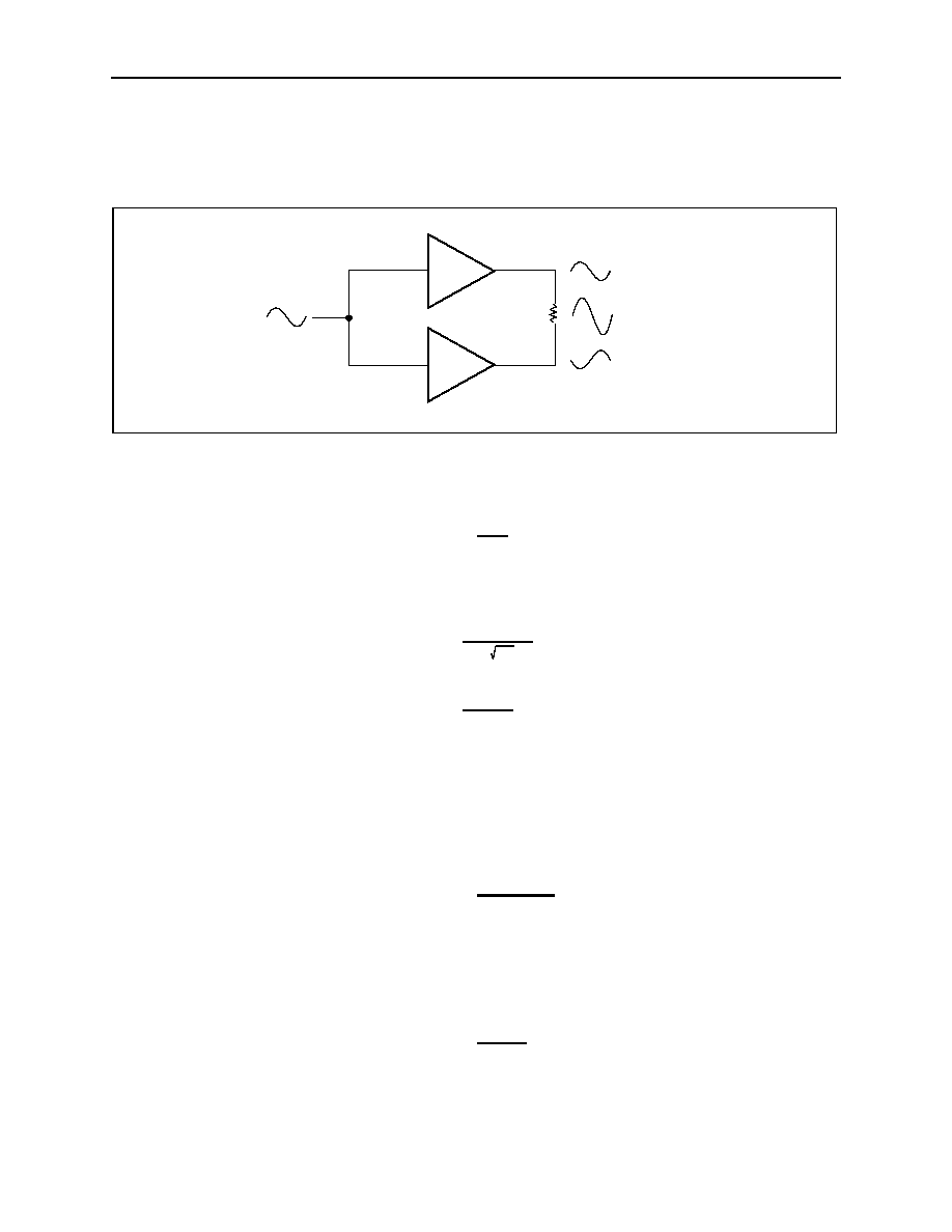
BTL Amplifier
7.1 BTL Amplifier
All devices are designed to drive loads differentially in a bridge-tied load (BTL) configuration.
Figure 4. Bridge Tied Load Configuration
The BTL configuration doubles the output voltage (illustrated in Figure 4) compared to a single-ended amplifier under
similar conditions. Thus, the differential gain of the device (A
VD
) is twice the closed-loop gain of the input amplifier. The
effective gain is given by:
Substituting 2 x V
OUT(P-P)
for V
OUT(P-P)
into (EQ 3) and (EQ 4) yields four times the output power due to doubling of
the output voltage:
Since the BTL outputs are biased at mid-supply, there is no net DC voltage across the load. This eliminates the need
for the large, expensive, performance degrading DC-blocking capacitors required by single-ended amplifiers.
7.2 Power Dissipation and Heat Sinking
Normally, the devices dissipate a significant amount of power. The maximum power dissipation is given in Table 1 as
Continuous Power Dissipation, or it can be calculated by:
where T
J(MAX)
is +150∞C, T
AMB
(see Table 1) is the ambient temperature, and
JA
is the reciprocal of the derating fac-
tor in ∞C/W as specified in Table 1. For example,
JA
of the TQFN package is +59.2∞C/W.
The increased power delivered by a BTL configuration results in an increase in internal power dissipation versus a sin-
gle-ended configuration. The maximum internal power dissipation for a given V
CC
and load is given by:
+1
-1
V
OUT(P-P)
V
OUT(P-P)
2 x V
OUT(P-P)
A
VD
= 2 x
R
IN
(EQ 2)
R
F
V
RMS
=
2 2
(EQ 3)
V
OUT(P-P)
P
OUT
=
R
L
(EQ 4)
V
RMS2
P
DISSPKF(MAX)
=
JA
(EQ 5)
T
J(MAX)
-T
A
P
DISSPKF(MAX)
=
2
R
L
(EQ 6)
2V
CC2

www.austriamicrosystems.com
Revision 1.01
8 - 13
AS1702, AS1703, AS1704, AS1705
austria
micro
systems
Data Sheet
Fixed Differential Gain (AS1703, AS1704, and AS1705)
If the internal power dissipation exceeds the maximum allowed for a given package, power dissipation should be
reduced by increasing the ground plane heat-sinking capabilities and increasing the size of the device traces (see Sec-
tion 7.5 Layout and Grounding Considerations on page 9). Additionally, reducing V
CC
, increasing load impedance, and
decreasing ambient temperature can reduce device power dissipation.
The integrated thermal-overload protection circuitry limits the total device power dissipation. Note that if the junction
temperature is
+145∞C, the integrated thermal-overload protection circuitry will disable the amplifier output stage. If
the junction temperature is reduced by 9∞, the amplifiers will be re-enabled.
Note: A pulsing output under continuous thermal overload results as the device heats and cools.
7.3 Fixed Differential Gain (AS1703
,
AS1704, and AS1705)
The AS1703, AS1704, and AS1705 contain different internally-fixed gains (see Ordering Information on page 12). A
fixed gain facilitates simplified designs, decreased footprint size, and elimination of external gain-setting resistors.
The fixed gain values are achieved using resistors R
1
and R
2
(see Figure 3 on page 6).
7.4 Adjustable Differential Gain (AS1702)
7.4.1 Gain-Setting Resistors
The AS1702 uses external feedback resistors, R
F
and R
IN
(Figure 5), to set the gain of the device as:
where A
V
is the desired voltage gain. For example, R
IN
= 10k
, R
F
= 20k
yields a gain of 2V/V, or 6dB.
Note: R
F
can be either fixed or variable, allowing the gain to be controlled by software (using a AS150x digital poten-
tiometer. For more information on the AS1500 family of digital potentiometers, refer to the latest version of the
AS150x data sheet, available from the austriamicrosystems website
http://www.austriamicrosystems.com
.)
Figure 5. Setting the AS1702 Gain
A
V
=
R
IN
(EQ 7)
R
F
AS1702
+
≠
OUT+
OUT-
R
F
20k
R
F
20k
Bias
Generator
Inverting Differential
Input
Non-Inverting Differential
Input
C
IN
*
10µF
C
IN
*
10µF
R
IN
10k
R
IN
10k
* Optional
C
BIAS
0.1µF
IN+
IN-

www.austriamicrosystems.com
Revision 1.01
9 - 13
AS1702, AS1703, AS1704, AS1705
austria
micro
systems
Data Sheet
Layout and Grounding Considerations
7.4.2 Input Filter
The BTL inputs can be biased at voltages other than mid-supply. However, the integrated common-mode feedback cir-
cuit adjusts for input bias, ensuring the outputs are still biased at mid-supply. Input capacitors are not required if the
common-mode input voltage (V
IC
) is within the range specified in Table 2 and Table 3.
Input capacitor C
IN
(if used), in conjunction with R
IN
, forms a high-pass filter that removes the DC bias from an incom-
ing signal. The AC coupling capacitor allows the amplifier to bias the signal to an optimum DC level. Assuming zero-
source impedance, the -3dB point of the high-pass filter is given by:
Setting f
-3dB
too high affects the low-frequency response of the amplifier. Capacitors with dielectrics that have low-volt-
age coefficients such as tantalum or aluminum electrolytic should be used, since capacitors with high-voltage coeffi-
cients, such as ceramics, can increase distortion at low frequencies.
7.4.3 BIAS Capacitor
BIAS is the output of the internally generated V
CC
/2 bias voltage. The BIAS bypass capacitor, C
BIAS
, improves PSRR
and THD+N by reducing power supply noise and other noise sources at the common-mode bias node, and also gener-
ates the click- and pop-less DC bias waveform for the amplifiers. Bypass BIAS with a 0.1µF capacitor to GND. Larger
values of C
BIAS
(up to 1µF) improve PSRR, but increase t
ON
/t
OFF
times. For example, a 1µF C
BIAS
capacitor increases
t
ON
/t
OFF
by 10 and improves PSRR by 20dB (at 1kHz).
Note: Do not connect external loads to BIAS.
7.4.4 Supply Bypassing
Proper power supply bypassing ≠ connect a 10µF ceramic capacitor (C
BIAS
) from V
CC
to GND ≠ will ensure low-noise,
low-distortion performance of the device. Additional bulk capacitance can be added as required.
Note: Place C
BIAS
as close to the device as possible.
7.5 Layout and Grounding Considerations
Well designed PC board layout is essential for optimizing device performance. Use large traces for the power supply
inputs and amplifier outputs to minimize losses due to parasitic trace resistance and route heat away from the device.
Good grounding improves audio performance and prevents digital switching noise from coupling onto the audio signal.
f
-3dB
=
(EQ 8)
1
2
R
IN
C
IN

www.austriamicrosystems.com
Revision 1.01
10 - 13
AS1702, AS1703, AS1704, AS1705
austria
micro
systems
Data Sheet
Pin Descriptions and Assignments
8 Pinout and Packaging
8.1 Pin Descriptions and Assignments
Figure 6. Pin Assignment (Top View)
Table 5. Pin Descriptions ≠ MSOP-10 Package
Pin
Name
Description
1
SHDN
Shutdown Input ≠ The polarity of this pin is dependent on the state of pin SHDM.
2
IN-
Inverting Input.
3
SHDM
Shutdown-Mode Polarity Input ≠ Controls the polarity of SHDN. Connect this pin
high for an active-high SHDN input. Connect this pin low for an active-low SHDN
input (see Table 4 on page 5).
4
IN+
Non-Inverting Input
5
BIAS
DC Bias Bypass
6
OUT-
Bridge Amplifier Negative Output
7
GND
Ground
8
N/C
Not connected. No internal connection.
9
V
CC
Power Supply
10
OUT+
Bridge Amplifier Positive Output
1
2
3
4
10
9
8
7
SHDN
IN-
SHDM
IN+
OUT+
V
CC
N/C
GND
AS1702
AS1703
AS1704
AS1705
5
BIAS
6
OUT-
MSOP-10 Package
(3mmx3mmx0.8mm)

www.austriamicrosystems.com
Revision 1.01
11 - 13
AS1702, AS1703, AS1704, AS1705
austria
micro
systems
Data Sheet
Package Drawings and Markings
8.2 Package Drawings and Markings
Figure 7. MSOP-10 Package
Notes:
1. All dimensions are in millimeters (angle in degrees), unless oth-
erwise specified.
2. Datums B and C to be determined at datum plane H.
3. Dimensions D and E1 are to be determined at datum plane H.
4. Dimensions D2 and E2 are for top package and D and E1 are for
bottom package.
5. Cross section A-A to be determined at 0.12 to 0.25mm from the
lead tip.
6. Dimensions D and D2 do not include mold flash, protrusion, or
gate burrs.
7. Dimension E1 and E2 do not include interlead flash or protrusion.

www.austriamicrosystems.com
Revision 1.01
12 - 13
AS1702, AS1703, AS1704, AS1705
austria
micro
systems
Data Sheet
9 Ordering Information
The AS1702, AS1703, AS1704, and AS1705 are available with adjustable or preset amplifier gain.
Part Number
Package Type Delivery Form
Gain
Description
AS1702-T
MSOP-10
Tape and Reel
Adjustable
Package Size = 3x3x0.8mm
AS1703-T
A
V
= 0dB
AS1704-T
A
V
= 3dB
AS1705-T
A
V
= 6dB

www.austriamicrosystems.com
Revision 1.01
13 - 13
AS1702, AS1703, AS1704, AS1705
austria
micro
systems
Data Sheet
Copyrights
Copyright © 1997-2005, austriamicrosystems AG, Schloss Premstaetten, 8141 Unterpremstaetten, Austria-Europe.
Trademarks Registered Æ. All rights reserved. The material herein may not be reproduced, adapted, merged, trans-
lated, stored, or used without the prior written consent of the copyright owner.
All products and companies mentioned are trademarks or registered trademarks of their respective companies.
Disclaimer
Devices sold by austriamicrosystems AG are covered by the warranty and patent indemnification provisions appearing
in its Term of Sale. austriamicrosystems AG makes no warranty, express, statutory, implied, or by description regarding
the information set forth herein or regarding the freedom of the described devices from patent infringement. austriami-
crosystems AG reserves the right to change specifications and prices at any time and without notice. Therefore, prior
to designing this product into a system, it is necessary to check with austriamicrosystems AG for current information.
This product is intended for use in normal commercial applications. Applications requiring extended temperature
range, unusual environmental requirements, or high reliability applications, such as military, medical life-support or life-
sustaining equipment are specifically not recommended without additional processing by austriamicrosystems AG for
each application.
The information furnished here by austriamicrosystems AG is believed to be correct and accurate. However,
austriamicrosystems AG shall not be liable to recipient or any third party for any damages, including but not limited to
personal injury, property damage, loss of profits, loss of use, interruption of business or indirect, special, incidental or
consequential damages, of any kind, in connection with or arising out of the furnishing, performance or use of the tech-
nical data herein. No obligation or liability to recipient or any third party shall arise or flow out of
austriamicrosystems AG rendering of technical or other services.
Contact Information
Headquarters
austriamicrosystems AG
A-8141 Schloss Premstaetten, Austria
Tel: +43 (0) 3136 500 0
Fax: +43 (0) 3136 525 01
e-mail:
info@austriamicrosystems.com
For Sales Offices, Distributors and Representatives, please visit:
http://www.austriamicrosystems.com
austria
micro
systems ≠
a leap ahead