 | –≠–ª–µ–∫—Ç—Ä–æ–Ω–Ω—ã–π –∫–æ–º–ø–æ–Ω–µ–Ω—Ç: AS2520 | –°–∫–∞—á–∞—Ç—å:  PDF PDF  ZIP ZIP |

Preliminary
AS2520/21/20B/21B
Rev. 5.1
Page 1
May 1999
Key Features
u
Line/speech circuit, loudhearing, handsfree and
dc/dc converter on one 28 pin CMOS chip
u
Operating range from 13 to 100 mA (down to 5
mA with reduced performance)
u
Soft clipping control eliminating harsh distortion
u
Volume control of receive signal with squelch and
automatic loop gain compensation
u
Line loss compensation pin selectable
u
Low noise (max. - 72 dBmp)
u
Real or complex impedance adjustable
u
NET 4 compatible
u
Dynamically controlled voice switching
u
Same monitor amplifier for loudhearing, handsfree
and tone ringer
u
Very few external components
u
Power derived from ring signal by switching
converter during ringing
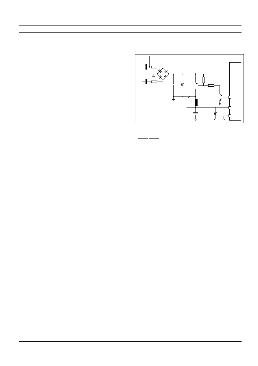
Typical Application
General Description
The AS2520/21/20B/21B are CMOS integrated
circuits that contain all the audio functions needed to
form a high comfort, line-powered telephone.
The devices incorporate line adaptation, speech
circuit, loudhearing and handsfree - all supervised by
the novel voice and power control circuit. A switching
converter is also provided for converting the ring
signal. The interface to a dialler/controller is made
very simple to allow easy adaptation to a telecom
microcontroller.
The AS2520 series incorporate volume control for the
earpiece and the loudspeaker (AS2520 digital with +/-
keys and AS2521 analogue with potentiometer). The
volume control circuit automatically compensates the
loop gain to ensure acoustic stability.
Package
Available in 28 pin SOP and DIP.
Lb
3V
La
AS2520
DIALLER
µCONTROLLER
LCD DRIVER
1
2
3
4
5
6
7
8
9
*
0
#
HSM
HFM
TELEPHONE
SPEECH CIRCUIT
WITH
LOUDHEARING,
HANDSFREE,
DC/DC CONVERTER
Figure 1: Typical Handsfree Telephone Application
Austria Mikro Systeme International AG
Telephone Speech Circuit
with Loudhearing and Handsfree

Preliminary
AS2520/21/20B/21B
Rev. 5.1
Page 2
May 1999
Pin Description
Pin #
Name
Type
Description
1
LS
AI
Line Current Sense Input
This input is used for sensing the line current.
2
CI
AI
Complex Impedance Input
Input pin for the capacitor in the complex impedance.
3
RO
AO
Receive Output
This is the output for driving a dynamic earpiece with an impedance of 140
to 300 ohm.
4
V
DD
Supply
Positive Voltage Supply
This is the supply pin for the circuit.
5
A
GND
Supply
Analogue Ground
This pin is the analogue ground for the amplifiers.
6
STB
AI
Side Tone Balance Input
This is the input for the side tone cancellation network.
7
LLC
DI
Line Loss Compensation Selection Pin
LLC = V
DD
:
High range
-6 dB from 45 mA to 75 mA;
LLC = A
GND
: Low range
-6 dB from 20 mA to 50 mA;
LLC = V
SS
: No regulation
gain independent of line current;
8
LSI
AO
Loudspeaker Amplifier Input
This is the input for applying the receive signal to the loudspeaker
amplifier.
9
TI
AI
DI
Tone Input
This switchable input is intended for transmitting DTMF or other signals
like messages on TAMs (Telephone Answering Machines) onto the line in
off-hook conditions and when in ringing mode to apply a PDM signal to the
loudspeaker (see also table 1).
10
RTH
AI
Receive Threshold Input
The sensibility of the receive peak detector can be adjusted by applying
the signal from RO to the RTH input through a voltage divider.
11
CM
AO
Converter Make Output
This is an output for controlling the external switching converter. It
converts the ring signal into a 4V supply voltage and is activated when PD
= high and HS, LE, MT = low.
12
V
PP
Supply
Loudspeaker Power Supply
High power supply for the output driver stage.
13
LO
AO
Output for Loudspeaker
Output pin for an ac coupled 32
(25 to 50
)loudspeaker.
14
V
SSP
Supply
Negative High Power Supply
This pin is the negative high power supply for the loudspeaker amplifier.
15
MT
DI
Mute Input
Dialling mute input (see also table 1).
MT = V
DD
: Tx and Rx channels muted;
MT = V
SS
: Tx and Rx channels not muted.
16
PD
DI
Power Down Input
Input for powering down the speech circuit and loudhearing/handsfree
(see table 1).
17
LE
DI
Loudhearing Enable Input
Input for enabling loudhearing/handsfree, active high (see table 1).
18
HS
DI
Handset Switch Input
This is an input that is pulled high by the hook switch (handset) or µC
when off-hook (see table 1).

Preliminary
AS2520/21/20B/21B
Rev. 5.1
Page 3
May 1999
19
22
M1
M2
AI
Microphone Inputs
Differential inputs for handset microphone (electret).
20
21
M4
M3
AI
Handsfree Microphone Inputs
These are the input pins for the handsfree microphone (electret).
23
VOL
D/AI
Volume Control Input
Volume control for the receive signal.
AS2520: Digital control with +/≠ keys or from µC;
AS2521: Analogue dc control with potentiometer.
24
SS
AO
Supply Source Control Output
This N-channel open drain output controls the external high power source
transistor for supplying (V
PP
) the loudspeaker amplifier in off-hook
loudhearing/handsfree mode.
25
CS
AO
Current Shunt Control Output
This N-channel open drain output controls the external high power shunt
transistor for the modulation of the line voltage and for shorting the line
during make period of pulse dialling.
26
V
SS
Supply
Negative Power Supply
27
LI
AI/O
Line Input
This input is used for power extraction and line current sensing.
28
RI
AI
Receive Input
This is the input for the receive signal.
DI:
Digital Input
AI:
Analogue Input
DO:
Digital Output
AO:
Analogue Output
DI/O:
Digital Input/Output
AI/O:
Analogue Input/output
Operating Modes
I/O Pins
Digital Inputs
Tone Input
Outputs
MODE
HS
LE
PD
MT
TI
CM
LI
RO
LO
Idle (on-hook)
0
0
0
0
Not connected
Low
-
PD
PD
Ringing
0
0
1
0
PDM signal to LO (DI)
SW
-
-
`TI'
POT
1
0
0
0
Not connected
Low
`M1/M2'
`RI/STB'
-
POT/pulse dialling
1
0
1
1
Not connected
Low
V
BE
-
-
POT/DTMF dialling
1
0
0
1
DTMF to LI and RO (AI)
Low
`TI'
`TI'
-
Handsfree
0
1
0
0
Not connected
Low
`M3/M4'
`RI/STB'
`LSI'
Handsfree/pulse dial
0
1
1
1
Not connected
Low
V
BE
-
Handsfree/DTMF dial
0
1
0
1
DTMF to LI and RO (AI)
Low
`TI'
`LSI'
Loudhearing
1
1
0
0
Not connected
Low
`M1/M2'
`RI/STB'
`LSI'
Loudhearing/pulse dial
1
1
1
1
Not connected
Low
V
BE
Loudhearing/DTMF dial
1
1
0
1
DTMF to LI and RO (AI)
Low
`TI'
`LSI'
TAM without LSP
1
0
1
0
Signal to LI (AI)
Low
`RI/STB'
TAM with LSP
1
1
1
0
Signal to LI (AI)
Low
`RI/STB'
`LSI'
Melody feedback
0
1
1
0
PDM signal to LO (DI)
Low
`RI/STB'
Test mode 1
0
0
0
1
Reserved for testing
Test mode 2
0
0
1
1
Reserved for testing
Table 1: Operating Modes

Preliminary
AS2520/21/20B/21B
Rev. 5.1
Page 4
May 1999
Functional Description
The AS252x contains all the voice circuits needed in
a high feature telephone instrument, i .e.:
∑
line adaptation (ac impedance, dc characteristics,
2/4-wire conversion, power extraction)
∑
handset speech circuit
∑
loudhearing with enhanced anti-Larsen
∑
handsfree with dynamic loop gain control
∑
switching converter
The line adaptation includes line driver, ac
impedance (return loss), 2 to 4 wire converter, dc
mask and power extraction circuit for extracting the
maximum dc power from the line to supply the whole
device and peripheral circuits.
The handset speech circuit consists of a transmit and
a receive path with mute, dual soft clipping and line
regulation (pin option). A volume control is provided
with squelch and loop gain compensation to improve
signal-to-noise ratio and to assure acoustic stability.
Loudhearing and handsfree functions are also
provided. The loudhearing function includes an anti-
Larsen circuit to prevent acoustic howling.
The handsfree circuit has a novel voice control
system which is virtually independent of any
background noise and works in a dynamic half
duplex mode as close to full duplex as the acoustic
loop gain allows.
The switching converter is used to extract the
available power from the ring signal and provides a
4V supply voltage. This allows the same loudspeaker
to be used for loudhearing/handsfree and tone
ringing.
LINE DRIVER
IMPEDANCE
SYNTESIZER
POWER
EXTRACTION
DC
CONTROL
VOICE
&
POWER
CONTROL
V
DD
TX-AGC
RX-AGC
V
DD
LE
HS
TI
LO
RO
A
GND
RTH
M2
M1
CI
LI
CS
LS
V
DD
Vss
RI
STB
A
GND
MT
MT or PD
30
L +
Z
B
AS2520/21/20B/21B
MT
V
PP
V
PP
PD
PD
LEVEL
DETECTOR
300
SS
SWITCHING
CONVERTER
CM
Vss
P
LSI
VOL
LOGIC
INTERFACE
LLC
LEVEL
DETECTOR
ST-AMP
RO-AMP
LO-AMP
MI-AMP
M3
MI-AMP
HS
M4
A
PDM
INPUT
RING
Figure 2: Block Diagramme

Preliminary
AS2520/21/20B/21B
Rev. 5.1
Page 5
May 1999
DC Conditions
The normal operating range (off-hook) is from 13 mA
to 100 mA. Operating range with reduced
performance is from 5 mA to 13 mA (parallel
operation). In the normal operating range all
functions are operational.
In the line hold range from 0 to 5 mA the device is in
a power down mode and the voltage at LI is reduced
to maximum 3.5V.
The dc characteristic (excluding diode bridge) is
determined by the voltage at LI and the resistor R1 at
line currents above 13 mA as follows:
V
LS
= V
LI
+ I
LINE
z R1
The voltage at LI is 4.5V.
Below 13 mA the AS252x provides an additional
slope in order to allow parallel operation (see figure
3).
100
90
80
70
60
50
40
30
20
10
0
0
1
2
3
4
5
6
7
8
(V)
VLS
VLI
(mA)
Line Current
Typically
No ac signals
Tamb: 25∞C
Figure 3: DC Mask
When the PD pin is high (during pulse dialling) the
speech circuit and other part of the device not
operating are in a power down mode to save current.
The CS pin is pulled to V
SS
in order to turn the
external shunt transistor on to keep a low voltage
drop at the LS pin during make periods.
AC Impedance
The synthesised ac impedance of the circuit is set on
chip and by an external resistor and an external
capacitor (for complex impedance).
When R1 is set to 30 ohm, the ac impedance is 1000
ohm real, and the complex part can be set by a
capacitor connected to pin 2 (CI).
For 600 ohm telephones it is recommended to
connect a resistor and a capacitor from pin LS to V
SS
(see application notes). The dc resistance of R1
should be kept at 30 ohm to ensure correct dc
condition.
Return loss and sidetone cancellation can be
determined independent of each other (see figure 4).
Speech Circuit
The speech circuit consists of a transmit and a
receive path with soft clipping, mute, line loss
compensation and sidetone cancellation.
Transmit
The gain of the transmit path is 36.5 dB in handset
mode (from M1/M2 to LS) and 46.5 dB in handsfree
mode (from M3/M4 to LS). The microphone inputs
have an input impedance of 15 kohm.
The unique dual soft clipping control circuit limits the
output voltage at LI to 2V
PEAK
. Dual means that the soft
clipping incorporates both a very fast control circuit to
eliminate harsh sidetone distortion and a slower
regulation circuit to limit the output voltage at 2V
PEAK
independent of the line impedance. The attack time
is 30 µs/6 dB. The overdrive range is 30 dB. When
mute is active, pin MT high, the gain is reduced by >
60 dB.
Receive
The gain of the receive path is 3 dB (test circuit
figure 8) from RI to RO. The receive input is the
differential signal of RI and STB. Also the receive
channel provides soft clipping to avoid acoustic
shock and harsh distortion.
When mute is active during dialling the gain is
reduced by > 60 dB. During DTMF dialling a MF
comfort tone is applied to the receiver. The comfort
tone is the DTMF signal with a level that is -30 dB
relative to the line signal.
Volume Control
On the AS2520 the receive gain can be changed by
pressing the volume keys. The + key increases the
gain by 10 dB in 5 steps and the ≠ key decreases the
gain by 10 dB in 5 steps. The gain is reset by next
off-hook. The volume can also be controlled via a
microcontroller.
The AS2521 uses a potentiometer to control the
receive gain. The volume is an indirect dc control to
avoid that noise is introduced from the potentiometer.
The volume control is common for both the earpiece
and the loudspeaker. Any increase will be
compensated to ensure acoustic stability.

Preliminary
AS2520/21/20B/21B
Rev. 5.1
Page 6
May 1999
The acoustic stability is provided as follows:
When the volume is increased, e.g. by 10 dB, the
receive gain maintains the same as long as no
receive signal is applied. Applying a receive signal
will cause a 10 dB increase of the receive gain and a
corresponding decrease of the transmit gain. This
squelch function improves the signal-to-noise ratio.
In other words, a certain increase of the volume
introduces a similar amount of dynamic voice
switching, controlled by the receive signal, also in the
handset mode.
Sidetone
A good sidetone cancellation is achieved by using
the following equation:
Z
BAL
/Z
LINE
= R5/R1
The sidetone cancellation signal is applied to the
STB input.
By using two separate Wheatstone Bridges for return
loss and sidetone cancellation it is very easy to
calculate the sidetone balance network (see figure 4).
This unique configuration provides a sidetone
cancellation less sensitive to tolerances on the
external balance network and totally independent of
the ac impedance and its tolerances.
A good and stable sidetone cancellation improves the
handsfree function considerably and ensures a safe
margin against acoustic instability under all
circumstances.
Z
LINE
R1
30 ohm
R5
300 ohm
Z
BAL
Figure 4: Sidetone Bridge
Furthermore, the dual Wheatstone bridge makes it
very simple to adapt the circuit to different PTT
requirements as these two parameters (return loss
and sidetone balance) are independent of each
other.
Line Loss Compensation
The line loss compensation (Rx and Tx AGC
controlled by the line current) is a pin option. When it
is activated, the transmit and receive gains are
changed by -6 dB in 1 dB steps at line currents from
20 to 50 mA or 45 to 75 mA depending on selected
range.
Loudhearing
The loudhearing mode is enabled when HS and LE
are high. In order to prevent acoustic coupling
between the handset microphone and the
loudspeaker, the AS252x incorporate an anti-Larsen
circuit.
The anti-Larsen circuit decreases the gain of the
loudspeaker amplifier when a microphone signal is
applied. If no signal is applied from the microphone,
the loudspeaker amplifier is at its full gain.
Anti-Clipping (not AS2520B/21B)
The anti-clipping circuit is activated in loudhearing
and handsfree mode. The circuit prevents harsh
distortion at very high signal levels.
Furthermore, the circuit assures that the integrity of
the whole telephone circuit is maintained under
extreme load conditions, since it prevents that the
supply voltage drops below a certain minimum level.
The attack time is fast (120 µs/6 dB) for preventing
harsh distortion when the amplitude rapidly
increases. For avoiding chopper effects and to
assure low distortion, the decay time is longer,
approx. 128 ms/6 dB.
When the anti-clipping circuit has been activated by a
large receive signal, the channel control will increase
the Tx gain corresponding to the reduction in Rx gain
caused by the anti-clipping.
Handsfree
The handsfree function allows voice communication
without using the handset (full 2-way speaker phone).
Two voice controlled attenuators prevent acoustic
coupling between the loudspeaker and the
microphone.
A conventional voice switching circuit has a channel
control with three states, namely idle, transmit or
receive. In idle state, when no signal is applied, both
the transmit and the receive channels are attenuated
by approx. 20 dB to keep the total loop gain below 0
dB.
When a signal is applied to the microphone, the
circuit switches to transmit state, i.e. the gain in the
transmit channel is increased and the gain in the
receive channel is decreased accordingly. And vice
versa when a receive signal is applied.

Preliminary
AS2520/21/20B/21B
Rev. 5.1
Page 7
May 1999
This approach has some disadvantages. It requires a
high degree of discipline, since the three state
channel control gives a very distinct half duplex with
a relative high switching time constant to avoid
chopper effects. Furthermore, the system is very
sensitive to the environment,- noise, line conditions
and acoustics (echo).
Apart from keeping a distinct discipline, the user can
not do anything to minimise the effect of these
constraints, since the parameters of the voice
switching (thresholds, time constants, noise
discrimination, etc.) can not be changed or adapted
to the actual conditions by the user.
The dynamic voice control system of the AS252x
have been designed to overcome the above
constraints. The basic philosophy behind the AS252x
is that telephone circuits should not have any
automatic regulations preventing the user from
having all information about the actual conditions
which should enable her/him to act accordingly, i.e.
to comply with the given constraints.
Now, assuming subscriber A has a handsfree
telephone and is calling subscriber B, who has a
normal telephone. The B subscriber does not
necessarily know that A is using a handsfree
telephone and will therefore not automatically comply
to the discipline of a half duplex conversation. Hence,
the disadvantages by using half duplex should apply
to the A subscriber only.
Secondly, if A is in a noisy environment, the B
subscriber should hear it, so that he speaks up to
increase the signal-to-noise ratio at the A subscriber.
The traditional 3-state switching system has two
major drawbacks: first of all, when no one is talking,
the circuit is in idle state and the B subscriber gets
the feeling that the line is dead, since the background
noise does not activate the voice switching.
Secondly, the B subscriber does not speak up, since
she/he does not hear the background noise.
The concept of the AS252x, however, does not
exclude the human factor, but provides the
information about the actual conditions to the user
and allows her/him to act accordingly, i.e. to speak
up, to change the volume, etc.
In more technical terms, the AS252x works in the
following manner:
When no signal is applied neither from the line nor
from the microphone, the circuit is in the only static
state, which is transmit channel full open and receive
channel attenuated by up to 30 dB.
The advantages of using the transmit state as the
static (idle) state are that the B subscriber hears an
open line (the line is not dead), does not miss the
initial word of a sentence when the A subscriber
starts talking, and hears the level of the background
noise at A¥s end which will actuate her/him to speak
up accordingly.
When the A subscriber starts talking, the circuit
remains in the static state.
The dynamic state of the voice switching can only be
activated by the receive signal. Applying a receive
signal above a certain level will cause the circuit to
enter the dynamic state.
VOL
Z
AC
S
I
D
E
T
O
N
E
V
TX
V
RX
V
LINE
± 10 dB
AGC
PEAK
DETECTOR
2/4
V
TH
Figure 5: Channel Control System
The signal for controlling the channel attenuation is
taken after the sidetone amplifier. With the volume at
0 dB (neutral) the threshold for entering the dynamic
state (V
TH
) is 15 mV assuming that V
RX
> V
TX
(see
figure 5).
In the dynamic state the channel attenuation is
controlled by a voltage controlled amplifier. The
attack time is 4 ms/6 dB and the hold time is 200 ms.
A speech compression is activated when a transmit
signal with a high amplitude reaches a level
corresponding to approximately 460 mV on the line.
1.50
1.25
1.00
0.75
0.50
0.25
0.00
0
50
100
150
200
250
300
Microphone Input Signal
L
i
n
e
O
u
t
p
u
t
S
i
g
n
a
l
(mV)
(mV)
Sidetone Cancellation: 11 dB
Volume Control: 0 dB (neutral)
Figure 6: Speech Compression
Preliminary
AS2520/21/20B/21B
Rev. 5.1
Page 8
May 1999
The speech compression allows a higher gain in the
transmit channel, i.e. the microphone gets more
sensitive at low sound pressure levels on the
microphone, which enables the user to move further
away from the telephone. This means that a constant
signal is provided on the line practical independent of
the microphone signal level. Any reduction of gain by
the compressor in the transmit channel will
automatically be given to the receive channel.
Switching Converter
The ac ringing signal is utilised to extract the power
necessary to the tone ringer circuit. A switch mode
power supply is used to obtain a high efficiency dc
conversion.
This approach allows the use of the same
loudspeaker and amplifiers for both loudhearing and
tone ringing. It also allows an acoustic feedback of
the melodies during programming with the same
sound pressure level as during ringing.
When a ringing signal is applied, PD is pulled high
and the oscillator is enabled. The switching converter
is controlled by the output CM, which is turned high
and low with a duty cycle controlled by the voltage at
V
PP
.
When off-hook the switching converter has a high
impedance (CM low) to avoid any influence on the
transmission and on pulse dialling.
The smoothing capacitor should be in the range of 10
to 68 nF. The choke coil must have an inductance of
>1mH and a dc resistance of < 15 ohm.
CM
V
PP
Vss
P
2.2 mH
BC
327
470 µ
La
Lb
1µ5
1µ5
510
510
5k6
33 n
10 k
A
S
2
5
2
x
5V1
V
PP
BC
547
30V
Figure 7: Switching Converter
Tone Input
The tone input is a digital input in ringing mode and
during melody feedback. The digital melody signal
(PDM = pulse density modulation) is directly applied
to the TI input (see also application notes for further
details).
During DTMF dialling the DTMF signal is applied
through a capacitor to the TI input and will be fed to
the line (pin LI) and to the receive output (RO) as
confidence tone.

Preliminary
AS2520/21/20B/21B
Rev. 5.1
Page 9
May 1999
Electrical Characteristics
Absolute Maximum Ratings*
Supply Voltage............................................................................................................................... -0.3
V
DD
7V
Input Current..........................................................................................................................................+/- 25 mA
Input Voltage (LS) ....................................................................................................................... -0.3V
V
IN
10V
Input Voltage (LI, CS, SS).............................................................................................................-0.3V
V
IN
8V
Input Voltage (STB, RI) .........................................................................................................-2V
V
IN
V
DD
+0.3V
Digital Input Voltage .......................................................................................................... -0.3V
V
IN
V
DD
+ 0.3V
Electrostatic Discharge ..........................................................................................................................+/- 1000V
Storage Temperature Range........................................................................................................... -65 to +125∞C
Total Power Dissipation ............................................................................................................................ 500mW
*Exceeding these figures may cause permanent damage. Functional operation under these conditions is not permitted.
Recommended Operating Range
Symbol
Parameter
Conditions
Min.
Typ.*
Max.
Units
V
DD
Supply Voltage (internally generated)
Speech mode
3.0
4.1
5.5
V
V
PP
Supply Voltage (internally regulated)
Speech mode
3.0
4.1
5.5
V
T
AMB
Ambient Operating Temp. Range
-25
+70
∞C
* Typical figures are at 25∞C and are for design aid only; not guaranteed and not subject to production testing.
DC Characteristics (I
LINE
= 15 mA, recommended operating conditions unless otherwise specified)
Symbol
Parameter
Conditions
Min.
Typ.
Max.
Units
I
DD
Operating Supply Current
HS = high
LE = high
HS and LE = high
PD = high, CM running
5
5
5
300
7
7
7
mA
mA
µA
µA
I
DDPD
I
DD0
Power-Down Current
Standby Current
PD = high
All digital inputs = V
SS
200
1
µA
µA
V
LI
Line Voltage
13 mA< I
LINE
< 100 mA
4.2
4.5
4.8
V
I
OL
Output Current, Sink
Pin CS, SS
V
OL
= 0.4V
1.5
mA
I
OL
Output Current, Sink
Pin CM
V
OL
= 0.4V
1.5
mA
V
IL
Input Low Voltage
T
AMB
= 25∞C
V
SS
0.2 V
DD
V
V
IH
Input High Voltage
T
AMB
= 25∞C
0.8 V
DD
V
DD
V

Preliminary
AS2520/21/20B/21B
Rev. 5.1
Page 10
May 1999
AC Electrical Characteristics
I
LINE
= 15 mA; f = 800 Hz; recommended operating conditions unless otherwise specified.
Transmit
Symbol
Parameter
Conditions
Min.
Typ.
Max.
Units
A
TX
Gain (M1/M2 to LS)
Gain (M3/M4 to LS)
HS, LH modes; LLC = A
GND
HF mode; LLC = A
GND
35
45
36.5
46.5
38
48
dB
dB
A
MF
Gain (TI to LS)
MF mode
12
13.5
15
dB
A
TX/F
Variation with Frequency
f = 500 Hz to 3.4 kHz
+/- 0.8
dB
A
LLC
Gain Range, LLC
Speech mode; LLC = V
SS
or V
DD
-6
dB
THD
Distortion
V
LI
< 0.25 V
RMS
2
%
V
AGC
V
AGC
A
SCO
Soft Clip Level
Soft Clip Level
Soft Clip Overdrive
HS, LH modes; V
LI
=
HF mode; V
LI
=
2
650
30
V
PEAK
mV
PEAK
dB
Z
IN
Input Impedance;
M1/M2 and M3/M4
15
kohm
A
AD
Attenuation Depth
30
dB
A
MUTE
Mute Attenuation
Mute activated
60
dB
V
NO
Noise Output Voltage
HS = high; T
AMB
= 25∞C
LE = high; HS = low; T
AMB
= 25∞C
-72
-62
dBmp
dBmp
V
IN MAX
Input Voltage Range;
M1/M2
Differential
Single ended
+/- 1
+/- 0.5
V
PEAK
V
PEAK
Line Driver
Symbol
Parameter
Test Conditions
Min.
Typ.
Max.
Units
V
IN MAX
Input Voltage Range; LI
+/- 2
V
PEAK
RL
Z
AC/TEMP
Return Loss
Temperature Variation
Z
RL
= 1000 ohm; T
AMB
= 25∞C
18
0.5
dB
/∞C

Preliminary
AS2520/21/20B/21B
Rev. 5.1
Page 11
May 1999
Receive
Symbol
Parameter
Condition
Min.
Typ.
Max.
Units
A
RX
Gain (LS to RO), Default
LSP Gain (LSI to LO)
Volume reset
1.5
17.5
3
19
4.5
20.5
dB
dB
A
TX/F
Variation with Frequency
f = 500 Hz to 3.4 kHz
+/- 0.8
dB
A
LLC
Gain Range, LLC
Speech mode; LLC = V
SS
or V
DD
-6
dB
A
RX
Volume Range
10 steps, each 2 dB
20
dB
THD
Distortion
V
RI
< 0.2 V
RMS
2
%
V
SC
A
SCO
Soft Clip Level (RO)
Soft Clip Level (LO)
Soft Clip Overdrive
V
RO
=
Not AS2520B/21B; V
LO
=
Unloaded
1
1.3
30
V
PEAK
V
PEAK
dB
V
RTH
A
AD
t
DECAY
t
DECAY
Threshold Voltage at RTH
Attenuation Depth
Attack Time
Decay Time
Channel control; V
RI
> 0.8 V
RMS
Channel control
7
15
30
25
mV
dB
µs/6dB
µs/6dB
V
NO
V
UFC
Noise Output Voltage (RO)
Unwanted Frequency
Components (RO)
HS = high; T
AMB
= 25∞C
50 Hz.........20 kHz
-72
-60
dBmp
dBmp
Z
IN
Input Impedance, RI
8
kohm
V
IN RI
Input Voltage Range, RI
+/- 2
V
PEAK
A
ST
Sidetone Cancellation
V
RI
< 0.2 V
RMS
; T
AMB
= 25∞C
26
dB
Z
IN
Input Impedance, STB
80
kohm
V
IN ST
Input Voltage Range, STB
+/- 2
V
PEAK
General Timings
Symbol
Parameter
Condition
Min.
Typ.
Max.
Units
t
VOL
Volume Key Debounce
7
ms
t
SCA
Soft Clip Attack Time
V
IN
above soft clip level
0.12
ms/6dB
t
SCD
Soft Clip Decay Time
V
IN
below soft clip level
128
ms/6dB
t
PDA
Peak Detector Attack Time V
IN
above V
TH
3.2
ms/V
t
PDD
Peak Detector Decay Time V
IN
below V
TH
29
ms/V
t
LPA
Low-Power Attack Time
V
PP
< 3.6V
250
ms/6dB
t
LPD
Low-Power Release
V
PP
> 3.6V
1
sec/6dB

Preliminary
AS2520/21/20B/21B
Rev. 5.1
Page 12
May 1999
Test Circuit
1
0
µ
L
S
R
I
S
T
B
L
I
C
S
V
s
s
P
D
M
1
M
2
R
O
M
4
H
S
A
G
N
D
V
P
P
V
D
D
R
T
H
M
3
L
O
L
S
I
T
I
V
O
L
L
E
M
T
L
L
C
AS252x
2
2
µ
3
0
o
h
m
3
0
0
o
h
m
6
k
1
0
µ
6
8
0
n
B
C
3
2
7
1
0
V
1
k
2
0
0
o
h
m
I
L
I
N
E
B
U
L
6
0
0
o
h
m
A
1
0
0
µ
C
M
C
I
2
2
µ
2
5
o
h
m
1
k
1
k
V
s
S
P
S
S
1
3
2
1
8
9
1
0
5
2
0
3
2
2
1
9
2
4
2
3
7
1
5
1
7
1
8
1
6
1
4
1
2
2
4
2
6
2
5
2
7
6
1
1
1
2
8
B
C
3
2
7
1
k
Figure 8: Test Circuit

Preliminary
AS2520/21/20B/21B
Rev. 5.1
Page 13
May 1999
Application Diagramme
A
S
2
5
2
x
L
I
N
E
A
D
A
P
T
E
R
/
T
E
L
E
P
H
O
N
E
V
O
I
C
E
C
I
R
C
U
I
T
TI
LI
La
Lb
Vss
CS
V
DD
PD
MT
RO
M1
CI
STB
LSI
A
GND
LS
RI
HS
LO
V
PP
CM
LE
M3
SS
RTH
V
SSP
M2
M4
LLC
15 n
10 n
300
1k8
7k5
10 µ
100 n
100 n
100 µ
32
470 µ
5k6
10 k
2N5551
2.2 mH
5V1
MPSA92
33 n
510
1µ5
510
1µ5
BC327
100 µ
33 n
10 µ
BC327
10 V
30
27
25
26
1
28
4
9
16
18
15
17
10
5
24
11
12
14
7
13
20
8
3
6
22
2
19
21
VOL
100 k
23
Side tone
balance
network
A
GND
15 n
100 n
100 n
2k2
1k2
1k2
220 µ
1 µ
INPUT FOR DTMF
AND
TONE RINGER MELODIES
CONTROL INPUTS
(FROM µC)
V
DD
V
DD
VOL+
VOL-
10 k
AS2521
AS2520
High
Low
Off
1k8
1k8
Figure 9: Application Diagramme
Applications Hints
Interface to Microcontroller
In off-hook condition the microcontroller can be supplied from V
DD
of AS252x. The digital inputs (HS, LE, PD, and
MT) must be kept low until V
DD
has reached its minimum operating voltage (>2.5V).
Radio Frequency Interference
The RFI sensitivity has been minimised by the consequent use of CMOS technology and one overall ground and
by having differential inputs with a relative low input impedance.
For further application information see application notes for the AS2520 series.
Preliminary
AS2520/21/20B/21B
Rev. 5.1
Page 14
May 1999
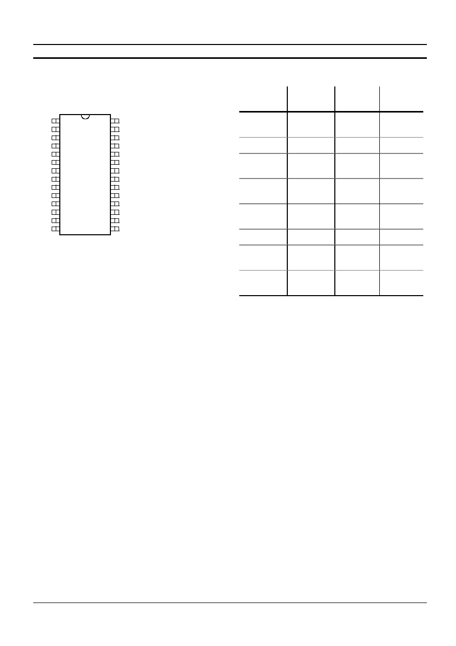
Pin Configuration
28 Pin SOP/DIP
1
2
3
4
5
6
7
8
9
10
11
12
13
14
LS
CI
RO
V
DD
A
GND
STB
LLC
RTH
LSI
TI
V
PP
LO
V
SSP
MT
RI
LI
V
SS
CS
SS
VOL
M2
M3
M4
CM
M1
HS
LE
A
S
2
5
2
x
PD
28
27
26
25
24
23
22
21
20
19
18
17
16
15
Ordering Information
Part
Number
Package
Type
Volume
Control
Soft Clip
Loudspk.
AS2520 T
28 pin
SOP
Digital
Yes
AS2520 P
28 pin DIP
Digital
Yes
AS2520B T
28 pin
SOP
Digital
No
AS2520B
P
28 pin DIP
Digital
No
AS2521 T
28 pin
SOP
Analogue
Yes
AS2521 P
28 pin DIP
Analogue
Yes
AS2521B T
28 pin
SOP
Analogue
No
AS2521B
P
28 pin DIP
Analogue
No
The devices are also available as dice on request.
Devices sold by Austria Mikro Systeme Int. AG are covered by the warranty and patent indemnification provisions appearing in
its Term of Sale. Austria Mikro Systeme Int. AG makes no warranty, express, statutory, implied, or by description regarding
the information set forth herein or regarding the freedom of the described devices from patent infringement Austria Mikro
Systeme Int. AG reserves the right to change specifications and prices at any time and without notice. Therefore, prior to
designing this product into a system, it is necessary to check with Austria Mikro Systeme Int. AG for current information. This
product is intended for use in normal commercial applications. Applications requiring extended temperature range, unusual
environmental requirements, or high reliability applications, such as military, medical life-support or life-sustaining equipment
are specifically not recommended without additional processing by Austria Mikro Systeme Int. AG for each application.
Copyright © 1999, Austria Mikro Systeme International AG, Schloss Premst‰tten, 8141 Unterpremst‰tten, Austria.
Trademarks RegisteredÆ. All rights reserved. The material herein may not be reproduced, adapted, merged, translated,
stored, or used without the prior written consent of the copyright owner.
Austria Mikro Systeme Int. AG reserves the right to change or discontinue this product without notice.