 | –≠–ª–µ–∫—Ç—Ä–æ–Ω–Ω—ã–π –∫–æ–º–ø–æ–Ω–µ–Ω—Ç: AS2524B | –°–∫–∞—á–∞—Ç—å:  PDF PDF  ZIP ZIP |

Revision 1.12, Preliminary
Page 1 of 19
austria
micro
systems
Key Features
-
Line/Speakerphone circuit on a 28-pin CMOS-IC, simple
inventory: same die for AS2523/24 and AS2523/24B
-
Serial I/F on AS2523, parallel I/F on AS2524
-
Enhanced voice switching
-
Background noise monitoring
-
Tx- and Rx-gain programmable on AS2523 only
-
Digital volume control of Rx signals on AS2523 only
-
DC characteristic programmable on AS2523 only
-
Dual softclipping in handset mode on AS2523 only
-
Dual softclipping in handsfree mode on AS2523 only
-
Loudspeaker amplifier for loudhearing and handsfree
-
Supply voltage generation for external circuitry
-
Automatic line loss compensation on AS2523 / 24B only
-
Real and complex impedance selectable by external
components
-
Side tone adaptation selectable by external components
-
Unique EMC performance
-
Operating range from 15mA to 100mA (down to 5mA
with reduced performance)
-
Few external components
General Description
AS2523/24 is a CMOS integrated circuit that incorporates
DC and AC line adaptation (DC-mask and synthesized AC-
impedance of 1000
) as well as a speech circuit with
softclipping, line loss compensation and Rx-volume control
for handset and handsfree operation. It shall act as an a/b-
line powered device, which is controlled by a CPU via a
serial interface on AS2523 or a standard dialler via a
parallel interface on AS2524 and AS2524B.
Applications
Enhanced handsfree feature phones with CallerID and
extended displays. The AS2524 and AS2524B are
developed to interface with common Taiwanese dialers.
Package
Available in 28-pin SOIC or die
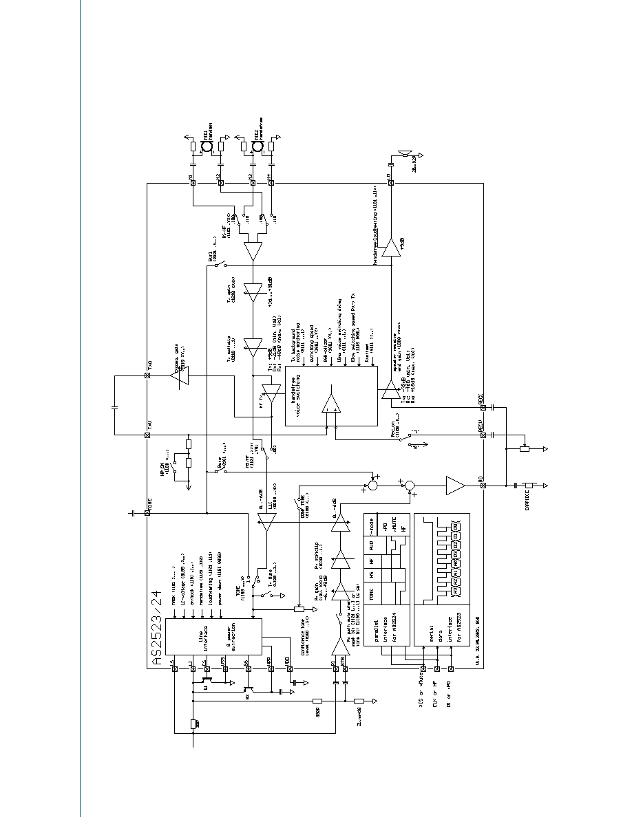
Block Diagram
Telephone Line Interface and
Speakerphone Circuit
AS2523, AS2524, AS2524B
PRELIMINARY DATA SHEET

Data Sheet AS2523, AS2524, AS2524B
austria
micro
systems
Revision 1.12, Preliminary
Page 2 of 19
Pin description
Pin #
Symbol
Function
15
LS
L
ine Current
S
ense Input
Analog input for sensing the line current
12
LI
L
ine
I
nput
Analog input used for power extraction and line current sensing
13
RI
R
eceive
I
nput
Analog input for ac-separated receive signal
9
STB
S
ide
T
one
B
alance Input
Analog input for side tone cancellation network
10
CS
C
urrent
S
hunt Control Output
N-channel open drain output to control the external high power shunt transistor for
synthesizing AC- and DC-impedance, modulation of line voltage and shorting the line during
make periods of pulse dialing
16
CI
C
omplex
I
mpedance Input
Analog input pin for the capacitor to program a complex impedance
14
SS
S
upply
S
ource Control Output
N-channel open drain output to control the external high power source transistor for supplying
(Vpp) the loudspeaker amplifier in off-hook loudspeaking/handsfree mode
11
VSS
V
oltage
S
ource
S
ource
Negative Analog Power Supply
18
VDD
V
oltage
D
rain
D
rain
Positive Analog Power Supply
19
AGND
A
nalog
G
round
Special ground for the internal amplifiers
8
M1
M
icrophone Input
1
Differential input for the handset microphone (electret)
6
M2
M
icrophone Input
2
Differential input for the handset microphone (electret)
7
M3
M
icrophone Input
3
Differential input for the handsfree microphone (electret)
5
M4
M
icrophone Input
4
Differential input for the handsfree microphone (electret)
17
RO
R
eceive
O
utput to
H
andset
Output for driving a dynamic earpiece with an impedance from 150
to 300

Data Sheet AS2523, AS2524, AS2524B
austria
micro
systems
Revision 1.12, Preliminary
Page 3 of 19
Pin #
Symbol
Function
25
xCS
C
hip
S
elect on AS2523
Chip select input of the serial interface. Internal pull-up resistor ( 100kOhm )
/xMUTE
Mute transmit-, receive- path and activate tone path on AS2524 and AS2524B
26
DI
D
ata
I
nput on AS2523
Data input of the serial interface. Internal pull-up resistor ( 100kOhm )
/xPD
Power down mode for AS2524 and AS2524B (On-hook)
27
CLK
Cl
oc
k
on AS2523
Clock input of the serial interface. Internal pull-up resistor ( 100kOhm )
/HFE
Handsfree mode operation on AS2524 and AS2524B
23
LO
L
oudspeaker
O
utput. Output pin is for a 25
loudspeaker
2
FT1
Analog input pin for connecting a capacitor for offset cancellation.
3
TXO
Analog output of the transmit signal
4
TXV
Analog input for the transmit signal in the voice switching path
1
CBN
Analog input pin for connecting a capacitor for background noise monitoring.
20
RECI
Analog input for the handsfree receive path. Should be connected to RO via coupling
capacitor.
21
RECV
Analog input for receive voice switching path.
24
VSSA
Power supply pin for LO output amplifier.
22
VPP
Power supply pin for LO output amplifier.
28
TONEIN Analog input for DTMF-signals.
Data Sheet AS2523, AS2524, AS2524B
austria
micro
systems
Revision 1.12, Preliminary
Page 4 of 19
Detailed Block Diagram
Data Sheet AS2523, AS2524, AS2524B
austria
micro
systems
Revision 1.12, Preliminary
Page 5 of 19
Functional Description
DC conditions
The normal operating mode is from 15mA to 100mA. An
operating mode with reduced performance is from 5mA to
15mA. In the line hold range from 0mA to 5mA the device
is in a power down mode.
The DC characteristic is determined by the voltage at LI-
pin and a 30
resistor between LI- and LS-pin. It can be
calculated by the following equation: V
LS
= V
LI
+ I
Line
*
30
. V
LI
can be programmed to be 3.5V or 4.5V.
2/4 wire conversion
AS2523/24 has built in two Wheatstone bridges with one
common ground. This provides a maximum of
independence of AC-impedance and side tone from each
other. One can adapt side tone without changing the AC-
impedance.
AC-impedance
The AC-impedance of AS2523/24 is set to t.m. 1000
.
With the external capacitor at CI-pin it can be programmed
complex. With an external resistor of approx. 1.5k
connected to the LS-pin it can be programmed to 600
.
Side Tone
A good side tone cancellation can be achieved by using the
following equation:
Z
BAL
/Z
LINE
= 10
Transmit path
The gain of the M1/M2
LS is set to +37dB. This gain
can be changed by programming on AS2523 from +30dB to
+45dB in 1dB steps (Register Txgain), on AS2524 / 24B it
is set to +37dB per default. The input is differential with an
impedance of 10k
. The soft clip circuit limits the output
voltage at LS to 2V
p.
There is LLC for this path.
The gain of the M3/M4
LS is set to +46dB.
This gain can be changed by programming from +39dB to
+54dB in 1dB steps on AS2523. The input is differential
with an impedance of 10k
. The soft clip circuit limits the
output voltage at LS to 2V
p
. There is no LLC for this path.
Receive path
The gain of the LS
RO receive path is set to +7.5dB.
This gain can be changed by programming from ≠7.5dB to
+7.5dB in 1dB steps (Register Rxgain). The receive input
is the differential signal of RI and STB. The soft clip circuit
limits the output voltage at RO to 1V
p.
It prevents harsh
distortion and acoustic shock. There is LLC for this path.
The gain of the LS
LO receive path is set to +32dB.
This gain can be changed by programming from +19dB to -
34dB in 1dB steps. The user can also change the gain via
Register Handsfree receive end gain (See section
"Handsfree"). The receive input is the differential signal of
RI and STB. The soft clip circuit limits the output voltage at
LO to 1.1V
p.
It prevents harsh distortion and acoustic
shock. There is optional LLC for this path.
Line Loss Compensation (AS2523, AS2524B)
-
programmable on AS2523
-
not activated at AS2524
-
permanently activated at AS2524B
When it is activated, the transmit and receive gains for
both I/O's are decreased by 6dB at line currents from
20mA to 50mA or from 45mA to 75mA.
Handsfree
The handsfree function allows voice communication without
using the handset (full 2-way speaker phone). Two voice
controlled attenuators prevent acoustic coupling between
the loudspeaker and the microphone. The voice switching
circuit has three states, namely idle, transmit or receive. In
receive mode the attenuation of the receive path and the
transmit path can be controlled by Register Handsfree
receive end gain between 0dB and -20dB. The following
table shows how voice switching is controlled
TX_atten
Backgnd
noise
monitor
Voice
switching
speech
RX
voice switching circuit