 | –≠–ª–µ–∫—Ç—Ä–æ–Ω–Ω—ã–π –∫–æ–º–ø–æ–Ω–µ–Ω—Ç: AS2524T | –°–∫–∞—á–∞—Ç—å:  PDF PDF  ZIP ZIP |

Revision 1.8, Preliminary
Page 1 of 19
austria
micro
systems
Key Features
-
Line/Speakerphone circuit on a 28-pin CMOS-IC, simple
inventory: same die for AS2523/24 and AS2523/24B
-
Serial I/F on AS2523, parallel I/F on AS2524
-
Enhanced voice switching
-
Background noise monitoring
-
Tx- and Rx-gain programmable on AS2523 only
-
Digital volume control of Rx signals on AS2523 only
-
DC characteristic programmable on AS2523 only
-
Dual softclipping in handset mode
-
Dual softclipping in handsfree mode
-
Loudspeaker amplifier for loudhearing and handsfree
-
Supply voltage generation for external circuitry
-
Automatic line loss compensation on AS2523 / 24B only
-
Real and complex impedance selectable by external
components
-
Side tone adaptation selectable by external components
-
Unique EMC performance
-
Operating range from 15mA to 100mA (down to 5mA
with reduced performance)
-
Few external components
General Description
AS2523/24 is a CMOS integrated circuit that incorporates
DC and AC line adaptation (DC-mask and synthesized AC-
impedance of 1000
) as well as a speech circuit with
softclipping, line loss compensation and Rx-volume control
for handset and handsfree operation. It shall act as an a/b-
line powered device, which is controlled by a CPU via a
serial interface on AS2523 or a standard dialler via a
parallel interface on AS2524 and AS2524B.
Applications
Enhanced handsfree feature phones with CallerID and
extended displays. The AS2524 and AS2524B are
developed to interface with common Taiwanese dialers.
Package
Available in 28-pin SOIC or die
Block Diagram
Telephone Line Interface and
Speakerphone Circuit
AS2523, AS2524, AS2524B
PRELIMINARY DATA SHEET

Data Sheet AS2523, AS2524, AS2524B
austria
micro
systems
Revision 1.8, Preliminary
Page 2 of 19
Pin description
Pin #
Symbol
Function
15
LS
L
ine Current
S
ense Input
Analog input for sensing the line current
12
LI
L
ine
I
nput
Analog input used for power extraction and line current sensing
13
RI
R
eceive
I
nput
Analog input for ac-separated receive signal
9
STB
S
ide
T
one
B
alance Input
Analog input for side tone cancellation network
10
CS
C
urrent
S
hunt Control Output
N-channel open drain output to control the external high power shunt transistor for
synthesizing AC- and DC-impedance, modulation of line voltage and shorting the line during
make periods of pulse dialing
16
CI
C
omplex
I
mpedance Input
Analog input pin for the capacitor to program a complex impedance
14
SS
S
upply
S
ource Control Output
N-channel open drain output to control the external high power source transistor for supplying
(Vpp) the loudspeaker amplifier in off-hook loudspeaking/handsfree mode
11
VSS
V
oltage
S
ource
S
ource
Negative Analog Power Supply
18
VDD
V
oltage
D
rain
D
rain
Positive Analog Power Supply
19
AGND
A
nalog
G
round
Special ground for the internal amplifiers
8
M1
M
icrophone Input
1
Differential input for the handset microphone (electret)
6
M2
M
icrophone Input
2
Differential input for the handset microphone (electret)
7
M3
M
icrophone Input
3
Differential input for the handsfree microphone (electret)
5
M4
M
icrophone Input
4
Differential input for the handsfree microphone (electret)
17
RO
R
eceive
O
utput to
H
andset
Output for driving a dynamic earpiece with an impedance from 150
to 300

Data Sheet AS2523, AS2524, AS2524B
austria
micro
systems
Revision 1.8, Preliminary
Page 3 of 19
Pin #
Symbol
Function
25
xCS
C
hip
S
elect on AS2523
Chip select input of the serial interface. Internal pull-up resistor ( 100kOhm )
/xMUTE
Mute transmit-, receive- path and activate tone path on AS2524 and AS2524B
26
DI
D
ata
I
nput on AS2523
Data input of the serial interface. Internal pull-up resistor ( 100kOhm )
/xPD
Power down mode for AS2524 and AS2524B (On-hook)
27
CLK
Cl
oc
k
on AS2523
Clock input of the serial interface. Internal pull-up resistor ( 100kOhm )
/HFE
Handsfree mode operation on AS2524 and AS2524B
23
LO
L
oudspeaker
O
utput. Output pin is for a 25
loudspeaker
2
FT1
Analog input pin for connecting a capacitor for offset cancellation.
3
TXO
Analog output of the transmit signal
4
TXV
Analog input for the transmit signal in the voice switching path
1
CBN
Analog input pin for connecting a capacitor for background noise monitoring.
20
RECI
Analog input for the handsfree receive path. Should be connected to RO via coupling
capacitor.
21
RECV
Analog input for receive voice switching path.
24
VSSA
Power supply pin for LO output amplifier.
22
VPP
Power supply pin for LO output amplifier.
28
TONEIN Analog input for DTMF-signals.

Data Sheet AS2523, AS2524, AS2524B
austria
micro
systems
Revision 1.8, Preliminary
Page 4 of 19
Detailed Block Diagram

Data Sheet AS2523, AS2524, AS2524B
austria
micro
systems
Revision 1.8, Preliminary
Page 5 of 19
Functional Description
DC conditions
The normal operating mode is from 15mA to 100mA. An
operating mode with reduced performance is from 5mA to
15mA. In the line hold range from 0mA to 5mA the device
is in a power down mode.
The DC characteristic is determined by the voltage at LI-
pin and a 30
resistor between LI- and LS-pin. It can be
calculated by the following equation: V
LS
= V
LI
+ I
Line
*
30
. V
LI
can be programmed to be 3.5V or 4.5V.
2/4 wire conversion
AS2523/24 has built in two Wheatstone bridges with one
common ground. This provides a maximum of
independence of AC-impedance and side tone from each
other. One can adapt side tone without changing the AC-
impedance.
AC-impedance
The AC-impedance of AS2523/24 is set to t.m. 1000
.
With the external capacitor at CI-pin it can be programmed
complex. With an external resistor of approx. 1.5k
connected to the LS-pin it can be programmed to 600
.
Side Tone
A good side tone cancellation can be achieved by using the
following equation:
Z
BAL
/Z
LINE
= 10
Transmit path
The gain of the M1/M2
LS is set to +37dB. This gain
can be changed by programming on AS2523 from +30dB to
+45dB in 1dB steps (Register Txgain), on AS2524 / 24B it
is set to +37dB per default. The input is differential with an
impedance of 10k
. The soft clip circuit limits the output
voltage at LS to 2V
p.
There is LLC for this path.
The gain of the M3/M4
LS is set to +46dB.
This gain can be changed by programming from +39dB to
+54dB in 1dB steps on AS2523. The input is differential
with an impedance of 10k
. The soft clip circuit limits the
output voltage at LS to 2V
p
. There is no LLC for this path.
Receive path
The gain of the LS
RO receive path is set to +9dB.
This gain can be changed by programming from -6dB to
+9dB in 1dB steps (Register Rxgain). The receive input is
the differential signal of RI and STB. The soft clip circuit
limits the output voltage at RO to 1V
p.
It prevents harsh
distortion and acoustic shock. There is LLC for this path.
The gain of the LS
LO receive path is set to +32dB.
This gain can be changed by programming from +19dB to -
34dB in 1dB steps. The user can also change the gain via
Register Handsfree receive end gain (See section
"Handsfree"). The receive input is the differential signal of
RI and STB. The soft clip circuit limits the output voltage at
LO to 1.1V
p.
It prevents harsh distortion and acoustic
shock. There is optional LLC for this path.
Line Loss Compensation (AS2523, AS2524B)
-
programmable on AS2523
-
not activated at AS2524
-
permanently activated at AS2524B
When it is activated, the transmit and receive gains for
both I/O's are decreased by 6dB at line currents from
20mA to 50mA or from 45mA to 75mA.
Handsfree
The handsfree function allows voice communication without
using the handset (full 2-way speaker phone). Two voice
controlled attenuators prevent acoustic coupling between
the loudspeaker and the microphone. The voice switching
circuit has three states, namely idle, transmit or receive. In
receive mode the attenuation of the receive path and the
transmit path can be controlled by Register Handsfree
receive end gain between 0dB and -20dB. The following
table shows how voice switching is controlled
TX_atten
Backgnd
noise
monitor
Voice
switching
speech
RX
voice switching circuit

Data Sheet AS2523, AS2524, AS2524B
austria
micro
systems
Revision 1.8, Preliminary
Page 6 of 19
0mV
~
100mV
RO
RECI
+3dB
+14dB
Voice
switching
speech
Gmax = -4dB ... +16dB (Vol)
Gmin = -33dB
Offset
comp
Compress
Peak
detector
Cmicoffset
+23dB
CBckgnd
Compress
Peak
detector
Compress
Peak
detector
LINE
Gmax = +9dB
Gmin = -21dB ... -40dB (Vol)
+9dB
RECV
FT1
CBN
+8dB
~
+17dB
TXO
TXV
Speech
Mode
Rx-gain
Tx-gain
Remark
Rx > Tx_atten
X
Receive
0db to -20dB
-50dB to -30dB
adjustable with VOL-setting
Tx_atten > Rx
NO
Idle
-25
-25
middle position
Tx_atten > Rx
YES
Transmit
-50dB
0dB
independent of VOL-setting
-50dB
-25dB
0dB
TX-mode
RX-mode
IDLE-mode
Vol min
Vol default
Vol max
TX-gain
RX-gain
-10dB
-20dB
-40dB
-30dB

Data Sheet AS2523, AS2524, AS2524B
austria
micro
systems
Revision 1.8, Preliminary
Page 7 of 19
Typical Characteristics of Line Loss Compensation (AS2523, AS2524B only)
The line-loss-compensation is programmable at the AS2523, not activated at the AS2524 and LLC high (45mA-75mA) activated
at the AS2524B.
Figure 1 Typical Tx Gain Characteristics Line Loss Compensation
Figure 2 Typical Rx Gain Characteristics Line Loss Compensation
f = 800 Hz
Z
LINE
= 600
V
LS
= -10 dBm
20
30
40
50
60
70
80
(mA)
DC Line
Current
No LLC (AS2523, AS2524)
LLC high
(AS2523,AS2524B)
LLC low
(AS2523)
Tx Gain
(dB)
29
30
31
32
33
34
35
f = 800 Hz
Z
LINE
= 600
V
LS
= -10 dBm
VOL = 0 dB (neutral)
20
30
40
50
60
70
80
(mA)
DC Line
Current
Rx Gain
(dB)
-2
-1
0
+1
+2
+3
+4
No LLC (AS2523, AS2524)
LLC high
(AS2523,AS2524B)
LLC low
(AS2523)
Data Sheet AS2523, AS2524, AS2524B
austria
micro
systems
Revision 1.8, Preliminary
Page 8 of 19
Serial Interface on AS2523
Registers
The settings of the AS2523 are stored in 16 registers. Each
register has 4 bit data width.
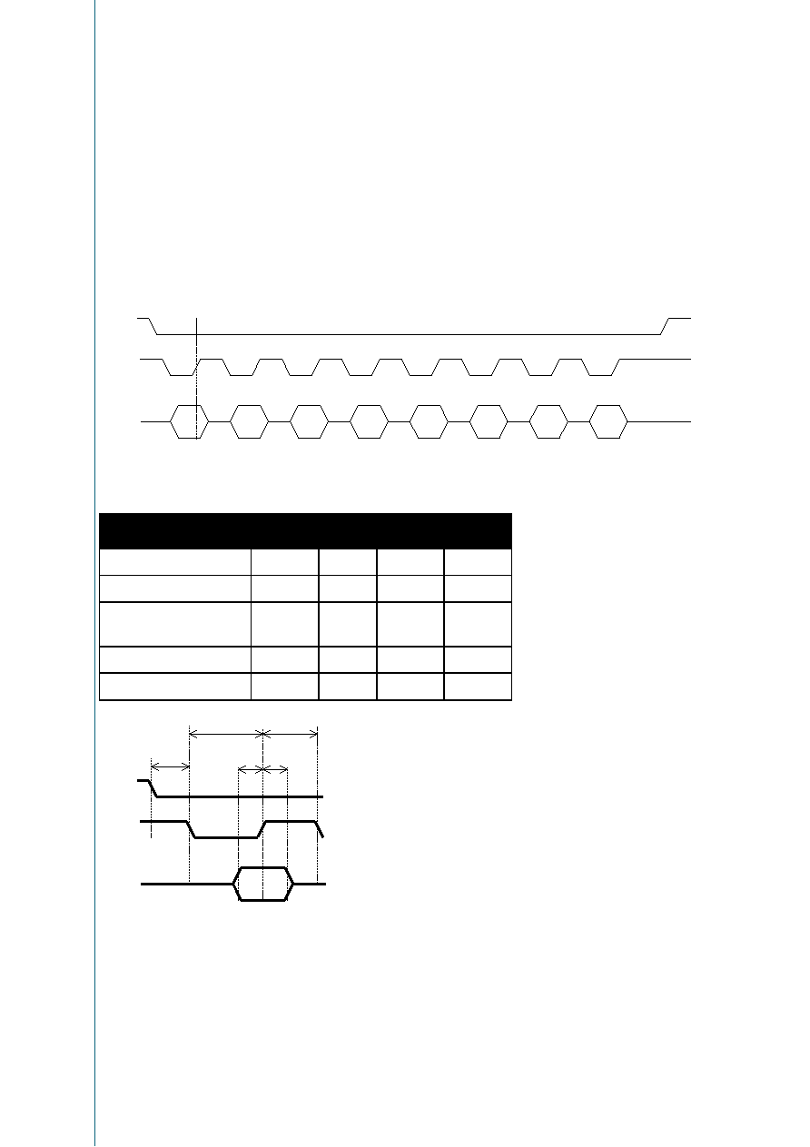
Timing
The data format for writing to a register has the following form:
A3
A2
A1
A0
D3
D2
D1
D0
xCS
CLK
DI
Note:
The pins xCS,CLK,DI have internal pull-up resistors.
Parameter
Symbol
MIN
TYP
MAX
CLK Pulse width HIGH
T6
100ns
CLK Pulse width LOW
T5
100ns
xCS to first falling CLK-
edge setup time
T1
50ns
DIN to CLK setup time
T3
50ns
DIN to CLK hold time
T4
50ns
t
1
xCS
CLK
DIN
t
3
t
4
t
5
t
6

Data Sheet AS2523, AS2524, AS2524B
austria
micro
systems
Revision 1.8, Preliminary
Page 9 of 19
Serial interface Registers
The following table shows the content of the 16 control registers.
For a detailed description of the commands see Application note AN523/24.
Control registers AS2523
A A A A D D D D
3 2 1 0
3 2 1 0
0 0 0 0
Nop
na
na
0 0 0 1
na
na
0 0 1 0
na
na
0 0 1 1
na
na
0 1 0 0
x x x x
Conf-Tone:
0... No Conf Tone 1... Conf Tone
0111
0111
Co
n
f
Li
v
Ll
c
1
Ll
c
0
LIV: Voltage at pin LI
0...3.5V, 1...4.5V
LLC1 LLC0: Line loss compensation setting
0
0
20mA-50mA
0
1
NO Line loss compensation
1
0
45-75mA
1
1
NO Line loss compensation
0 1 0 1
Bur
s
Bur
l
CT
1
CT
0
BURS: Analog tone at RO
0...OFF,
1...ON
BURL: Analog tone at LS
0...OFF,
1...ON
CT1 CT0: @RO
@LS
0
0
-36dB
-15dB
TONE-confidence level
0
1
-30dB
-9dB
rel. to pin LS
1
0
-24dB
-3dB
1
1
-18dB
+3dB
0001
0001
0 1 1 0
x x x x
Softclip-settings, Tx_comp_gain settings
1000
1000
t
x
_com
p_gai
n Bi
t
1
t
x
_com
p_gai
n Bi
t
0
S
o
ft-
R
X
S
o
ft-
T
X
Bit1 Bit0 :Tx_comp_gain
0
0
+8dB
0
1
+11dB
1
0
+14dB
1
1
+17dB
SOFTRX: Softclip RX
0...OFF,
1...ON
SOFTTX: Softclip TX
0...OFF,
1...ON
0 1 1 1
R
x
of
f
s
et
B
i
t
1
R
x
of
f
s
et
B
i
t
0
De
l
a
y
_
1
0
m
s
Bnon
Bit1 Bit0: Rx-offset setting
0
0
0mV
0
1
12mV
1
0
40mV
1
1
100mV
Delay_10ms
0... no delay
1... 10ms delay
Bnon
0... BGN off
1... BGN on
0101
1100
1 0 0 0
16 gains
Handsfree receive endgain
1111
1011
Data
RXgain
TXgain
0x0
-20dB
-30dB
Min. receive volume
:
:
0xF
+0dB
-50dB
Max. receive volume
1 0 0 1
x x x x
0000
1100
off1 off0: BGN-offset
0
0
120mV
0
1
180mV
1
0
240mV
1
1
300mV
of
f
1
of
f
0
Hf
s
1
Hf
s
0
Hfs1 HFs0: Speed of voice switching
0
0
max speed
0
1
1
0
1
1
min speed
1 0 1 0
16 gains
Transmit gain [16], 16 steps, 1dB stepsize
0111
0111
Data
HS-mode
HF-mode
0x0
30dB
39dB
:
:
:
0xF
45dB
54dB
1 0 1 1
16 gains
Receive gain [16], 16 steps, 1dB stepsize
1111
1111
Data
HS-mode
HF-mode
0x0
-6dB
19dB
:
:
:
0xF
+9dB
34dB
Address
Data
for AS2523,
AS2524HF
for AS2524 LH bond
option
Default value
after reset
1 1 0 0
HP
_
o
n
R
e
c_on
Mu
t
e
Tone
HP_on
:
0... fg=200Hz
1... fg=2000Hz
rec_on :
0... Rxcomp=AGND
1... Rxcomp=RECV
Mute
:
0... No mute
1... Tx-path muted
Tone
:
0... Tx-signal path 1... Ton in signal path
0100
1000
1 1 0 1
x x x x
Mask, Lh, Hf, Hook Switch
0100
0101
Mask:
0... No mask
1... Mask acitivated
Ma
s
k
His
Hf
LH
His
HF
LH: Hook functions
0
x
x
Power down
1
0
0
Handset
1
0
1
not allowed
1
1
0
Handsfree
1
1
1
Loudhearing
1 1 1 0
x x x x
0000
0001
Kr
at
5
Test
3
Test
2
sl
ow
_
r
ec
slow_rec: fast change to TX, slow change to RX, no IDLE
Krat5,Test3,Test2: For factory test only !
1 1 1 1
x x x x
Reset to defaults
na
na

Data Sheet AS2523, AS2524, AS2524B
austria
micro
systems
Revision 1.8, Preliminary
Page 10 of 19
Programming Guidelines for the AS2523
The AS2523 is programmed by means of a serial 8-bit shift
register. MSB is clocked in first, LSB last.
The first four bits (7,6,5,4) are the addresses of the
registers, the last four bits (3,2,1,0) are the data bits.
Each register has a default setting (see data sheet), which
is set after power-up of the chip.
The internal registers are RAM-cells. When the AS2523
loses VDD (as in on-hook state) it also loses the register
contents.
It is therefore necessary to re-write the affected registers
after each hook event. The register contents cannot be
read, they can only be written.
Registers need to be re-written after each power-up and
after each hook event (handset / handsfree / on-hook).
It is recommended to always initialize the chip with a "reset
to defaults command" (Fx) first and then write the
appropriate registers that need to be changed from the
default setting.
Alternatively, all registers (4 to 16) may be re-written in a
bulk at each power-up and hook event (handset /
handsfree / on-hook).
This guarantees safe operation in case of unexpected loss
of power during normal operation. Re-writing all registers
also eases later software updates, as only register
contents need to be changed, but no additional command
lines need to be inserted.
Example of a typical power-up sequence
A typical power-up sequence will require the following
programming.
a) determine the cause of power-up (handset / handsfree
mode) and set register D accordingly.
Default = handset mode
b) Set the LI voltage to 3.5V or 4.5V (default = 4.5V) and
Line Loss Compensation (default = off) in register 4
c) Set the Confidence Tone level (e.g. the DTMF level
which is audible in the handset) and path in register 5
Default = off
d) Set the required Tx and Rx gains in Registers A and B
Default = 37dB Tx gain, 1dB Rx gain
Additional settings in Handsfree mode
Note: change the default settings only if necessary:
a) A click-free startup can be achieved by starting up in
handset mode (=default) and then switching to
handsfree, once the chip has stabilized.
b) Change the Tx comparator preamplifier gain in register 6
Default = 14dB
c) Change the Receive DC offset and Background noise
monitoring in Register 7
default = 0mV offset (higher val. puts more weight on Rx)
switching delay default = on
Background Noise Monitoring = on
d) Set the speaker amplifier volume in register 8
Default = 0B
e) Set the handsfree voice switching speed and
Background Noise monitoring offset in register 9:
default voice switching speed = 1ms/6dB (fastest)
default BGN monitoring offset = 240mV (determines the
Tx level required to switch from idle to Transmit)
Additional settings during Flash
During a Flash, the AS2523 should be powered down to
avoid discharge of VDD:
Set the MASK bit (bit3 in register D) to 1
After the line current is restored, the MASK bit must be
cleared again. Other settings do not need to be re-written,
as VDD has not discharged. As a safety margin however, it
is recommended to re-write all registers after a flash
Additional settings during line breaks
If a line-break-detection (brief interruption of the line while
in off-hook state) is implemented, the same rules apply as
for a Flash: set the MASK bit to 1 to avoid discharge of
VDD. It is recommended to re-write all registers after a
line-break, as a line break may take long enough to
discharge VDD, even when the MASK bit was set.
General Rules
The serial interface may be programmed at any time, it
does not affect the speech quality, e.g. if a register is
overwritten with the same value.
It is also possible to re-write all registers periodically. The
register is static, therefore it can be clocked at any speed
up to 5MHz.
However, electromagnetic pulses on the clock and data
lines may cause unwanted programming of the chip. It is
therefore recommended to keep these lines short, filter
them by a discrete lowpass filter and reduce the clock
speed accordingly.

Data Sheet AS2523, AS2524, AS2524B
austria
micro
systems
Revision 1.8, Preliminary
Page 11 of 19
Parallel Interface on AS2524 and AS2524B
Input Signal on Pin
xPD
xMute
HF
Mode
0
0
0
Power down
0
0
1
Power down
0
1
0
Power down
0
1
1
Power down
1
0
0
Tone mode
1
0
1
Tone mode
1
1
0
Handset mode
1
1
1
Handsfree mode
Power down mode
For low power consumption the analog part is turned off during activated power down mode. The Power down mode is used
during Flash and Pulse dialing and for On-hook operation.
Handset mode
Speech mode is Handset mode (M1-M2, RO active; LO deactivated)
Parameter
AS2524
AS2524B
LI Voltage
4.5V
4.5V
LLC
No LLC
LLC high (45mA to 75mA)
TX-Gain
+37dB
+43dB
RX-Gain
+9dB
+9dB
Rx-Softclip
Off
On
Tx-Softclip
Off
Off
Tone
Off
Off
Handsfree mode
Speech mode is Handsfree mode (M3-M4, RO active; LO active)
Parameter
AS2524
AS2524B
LI Voltage
4.5V
4.5V
LLC
No LLC
LLC high (45mA to 75mA)
HF TX-Gain
+46dB
+52dB
HF RX-Gain
+34dB
+34dB
Rx-Softclip
Off
On
Tx-Softclip
Off
Off
Tone
Off
Off
BNM
On
On

Data Sheet AS2523, AS2524, AS2524B
austria
micro
systems
Revision 1.8, Preliminary
Page 12 of 19
Tone mode
This mode is used to send DTMF and FSK data to the line.
Speech mode is Tone mode (M1-M2;M3-M4 muted, Rx path muted, RO and LO active)
Parameter
AS2524
AS2524B
LI Voltage
4.5V
4.5V
LLC
No LLC
LLC high (45mA to 75mA)
Tone TX-Gain
+14dB
+14dB
Confidence tone
level
-36dB@Ro ≠15dB@Lo
relative to Pin LS
-36dB@Ro ≠15dB@Lo
relative to Pin LS
Loudhearing AS2524 and AS2524B (feature only available as DIE)
Speech mode is Loudhearing (M3-M4, RO active; LO activated).
Loudhearing can be activated via a bond-option (see document "AS2523/24 Delivery as Dice").
Parameter
AS2524
AS2524B
LI Voltage
4.5V
4.5V
LLC
No LLC
LLC high (45mA to 75mA)
TX-Gain
+37dB
+43dB
RX-Gain
+9dB
+9dB
Tone
Off
Off
Slow_rec
On
On
RECV pin
Deactivated
Deactivated
Highpass
2000kHz (10nF from TXO->TXV)
2000kHz (10nF from TXO->TXV)
Voice switching speed
120ms/6dB
120ms/6dB
RX-Offset
300mV
300mV
Electrical characteristics
Electrical characteristics are measured with the Test Circuit
application. Typical mean values will not be tested.
Absolute maximum ratings
Positive Supply Voltage
-0.3V <= V
DD
<= 7V
Input Current
+/- 25mA
Input Voltage (LS)
-0.3V <= V
in
<= 12V
Input Voltage (LI, CS)
-0.3V <= V
in
<= 8V
Input Voltage (STB, RI)
-2V <= V
in
<= V
DD
+0.3V
Digital Input Voltage
-0.3V <= V
in
<= V
DD
+0.3V
Electrostatic Discharge (HBM 1.5k
-100pF)
+/- 1000V
Storage Temperature
-65∞C to +125∞C
Recommended operating conditions
Supply Voltage (generated internally)
3V <= V
DD
<= 5V
Operating Temperature
-25∞C to +70∞C

Data Sheet AS2523, AS2524, AS2524B
austria
micro
systems
Revision 1.8, Preliminary
Page 13 of 19
DC characteristics
I
Line
=15mA w/o operation of any additional external
circuitry, unless other specified
Symbol
Parameter
Conditions
Min
Type
Max
Units
Test
I
DDS
Operating Current
Speech Mode
3
6
mA
Y
I
DDH
Operating Current
Handsfree Mode
7
10
mA
Y
V
LI
Line Voltage LIVolt=0
Line Voltage LIVolt=1
15mA<=ILINE<=100mA
3.2
4.2
3.5
4.5
3.8
4.8
V
V
Y
Y
I
OL
Output Current, Sink
CS,SS
VOL=0.4V
1
mA
N
Transmit characteristics
I
Line
=15mA f=800Hz, default settings unless other specified
Symbol
Parameter
Conditions
Min
Type
Max
Units
Test
A
M1/2TX
Transmit Gain M1/M2
LS
AS2524
AS2524B
Z
AC(syn)=
1000
35
39
+36.5
+42.5
38
44
dB
dB
Y
Y
A
M3/4TX
Transmit Gain M3/M4
LS
AS2524
AS2524B
Z
AC(syn)
=1000
43
49
+45.0
+51
47
53
dB
dB
Y
Y
A
tone TX
Transmit Gain
Tone
LS
Z
AC(syn)
=1000
12
+14dB
16
dB
Y
A
TX
Variation with frequency
f = 500Hz ... 3.4kHz
±0.8
dB
N
A
VRM12
Control range
M1/M2
LS
16 steps
-7/+8
dBr
N
A
VRM34
Control range
M2/M4
LS
16 steps
-7/+8
dBr
N
THD
Distortion
V
LS
=0.25VRMS
2
%
Y
V
AGC1
Soft Clip Level
M1/M2
LS at LS
2
VP
N
V
AGC2
Soft Clip Level
M3/M4
LS at LS
2
VP
N
A
SCO
Soft Clip Overdrive
M1/M2 - M3/M4
20
dB
N
t
attack
Attack time
70
us/6dB
N
t
decay
Decay time
100
ms/6dB
N

Data Sheet AS2523, AS2524, AS2524B
austria
micro
systems
Revision 1.8, Preliminary
Page 14 of 19
Symbol
Parameter
Conditions
Min
Type
Max
Units
Test
Z
IN-M1/2
Input Impedance
M1/M2
10
k
N
Z
IN-M3/4
Input Impedance
M3/M4
10
k
N
V
INmax
Input Voltage Range
M1/2 - M3/4
differential
±1
Vp
N
V
NO
Noise Output Voltage
LS
T
AMP
=25∞C
Handset mode
Gain = 36.5dB
-72
dBmp
Y
A
MUTE
Mute Attenuation
Mute activated
60
dB
Y
Receive characteristics
I
Line
=15mA f=800Hz, default settings unless other specified
Symbol
Parameter
Conditions
Min
Type
Max
Units
Test
A
RO
Receive Gain
LS
RO
Z
AC(syn)
=1000
Vol default
7.5
+9
10.5
dB
Y
A
LO12
Receive Gain
LS
LO
Z
AC(syn)
=1000
Vol maximum
+32.5
+34
+35.5
dB
Y
A
RX
Variation with frequency
f=500Hz to 3.4kHz
±0.8
dB
N
A
VRRO
Control range
LS
RO
16 steps
-7/+8
dBr
N
A
VRLS
Control range
LS
LO
16 steps
-7/+8
dBr
N
THD
LS
Distortion LO
V
LS
=0.25VRMS
5
%
Y
THD
RO
Distortion RO
V
LS
=0.25VRMS
2
%
Y
V
UFC
Unwanted Freq. Cmp.
f = 200 ... 20kHz
-60
dBm
Y
V
AGCRO
Soft Clip Level
RO
1
VP
N
V
AGCLS
Soft Clip Level
LO
1.1
VP
N
A
SCLS
Soft Clip Overdrive
LO
10
dB
N
T
attack
Attack time
70
us/6dB
N
T
decay
Decay time
100
ms/6dB
N

Data Sheet AS2523, AS2524, AS2524B
austria
micro
systems
Revision 1.8, Preliminary
Page 15 of 19
Symbol
Parameter
Conditions
Min
Type
Max
Units
Test
V
NO
Noise Output Voltage
RO
T
AMP
=25∞C
Gain = 3dB
-72
dBmp
Y
Z
IN-RI
V
INmax
Input Imp. RI
Input Voltage Range RI
8
±2
k
Vp
N
Z
IN-STB
V
INmax
Input Imp. STB
Input Volt. Range STB
80
±2
k
Vp
N
ST
Side tone
V
RI
<=0.25VRMS
26
dB
Y
RL
Z
AC/∞C
Return Loss
Temp. Variation
Z
AC(syn)
=1000
18
0.5
dB
/∞C
Y
Test circuit
VSS
R2 32R
C2
1uF
VSS
VSS
U2
AS2523/24
17
20
21
23
25
26
27
1
4
3
2
19
18
22
14
24
11
16
10
9
12
13
15
28
7
5
8
6
RO
RECI
RECV
LO
xCS / xMUTE
DI / xPD
CLK / HFI
CBN
TX
V
TX
O
FT
1
AG
N
D
VD
D
VPP
SS
VSSA
VSS
CI
CS
STB
LI
RI
LS
TONE IN
M3
M4
M1
M2
C2
2
2
u
F
R1
600R
D1
10V
VSS
C6 100nF
C6 100nF
R1
6k
C6 100nF
C2 1uF
Q1
BC327
D1
5V1
VSS
V3
Vac
C2
1
u
F
C6 100nF
VSS
R1
30R
C2 10uF
Vac
VSS
VSS
1
2
3
VSS
C2
10
0
u
F
Vac
C3
1n
VSS
Q1
BC327
C6 100nF
VSS
C4 100nF
VSS
VSS
VSS
VSS
C6 100nF
Vac
R3
150R
C1 10uF
C2
10
0u
F
I1
Idc
C2
47uF
VSS
R1
300R
C7 100uF
R5
10k
R4
10k

Data Sheet AS2523, AS2524, AS2524B
austria
micro
systems
Revision 1.8, Preliminary
Page 16 of 19
Typical application AS2523

Data Sheet AS2523, AS2524, AS2524B
austria
micro
systems
Revision 1.8, Preliminary
Page 17 of 19
Typical application AS2524 and AS2524B

Data Sheet AS2523, AS2524, AS2524B
austria
micro
systems
Revision 1.8, Preliminary
Page 18 of 19
Packaging
28-pin plastic SOIC
For exact mechanical package dimensions please see
austriamicrosystems
AG
packaging information.
Pin-out, Marking
YY
year of production
WW
calendar week of production
AAA
austriamicrosystems
AG
assembly ID
X
3 ... AS2523 Version
4 ... AS2524 Version
4B .. AS2524B Version
Ordering Information
Number
Package
Description
AS2523 T
SOIC28
plastic surface mounted
package ≠ 28 leads
AS2524 T
SOIC28
Plastic surface mounted
package ≠ 28 leads
AS2524B T
SOIC28
Plastic surface mounted
package ≠ 28 leads
AS2523 F
DOF
Dice-on-Foil
AS2524 F
DOF
Dice-on-Foil
AS2524B F
DOF
Dice-on-Foil
Devices sold by austriamicrosystems AG are covered by
the warranty and patent identification provisions appearing
in its Term of Sale. austriamicrosystems AG makes no
warranty, express, statutory, implied, or by description
regarding the information set forth herein or regarding the
freedom of the described devices from patent infringement.
austriamicrosystems AG reserves the right to change
specifications and prices at any time and without notice.
Therefore, prior to designing this product into a system, it
is necessary to check with austriamicrosystems AG for
current information. This product is intended for use in
normal commercial applications. Applications requiring
extended temperature range, unusual environmental
requirements, or high reliability applications, such as
military, medical life-support or life-sustaining equipment
are specifically not recommended without additional
processing by austriamicrosystems AG for each
application.
Copyright
Copyright © 1997-2002, austriamicrosystems AG, Schloss
Premstaetten, A8141 Unterpremstaetten, Austria-Europe.
Trademarks Registered Æ. All rights reserved. The material
herein may not be reproduced, adapted, merged,
translated, stored, or used without the prior written consent
of the copyright owner.
The information furnished here by austriamicrosystems AG
is believed to be correct and accurate. However,
austriamicrosystems AG shall not be liable to recipient or
any third party for any damages, including but not limited
to personal injury, property damage, loss of profits, loss of
use, interruption of business or indirect, special, incidental
or consequential damages, of any kind, in connection with
or arising out of the furnishing, performance or use of the
technical data herein. No obligation or liability to recipient
or any third party shall arise or flow out of
austriamicrosystems AG rendering of technical or other
services.
YYW
W
AAA
AS
2
5
2
X
15 LS
16 CI
17 RO
18 VDD
19 AGND
20 RECI
21 RECV
22 VPP
23 LO
24 VSSA
25 xCS/ xMUTE
26 DI / xPD
27 CLK / HFI
28 TONE IN
SS 14
RI 13
LI 12
VSS 11
CS 10
ST B 9
M1 8
M3 7
M2 6
M4 5
TXV 4
TXO 3
FT 1 2
CBN 1

Data Sheet AS2523, AS2524, AS2524B
austria
micro
systems
Revision 1.8, Preliminary
Page 19 of 19
Contact
Headquarters
austriamicrosystems AG
Communications Business Unit
A8141 Schloss Premstaetten, Austria
T. +43 (0) 3136 500-0
F. +43 (0) 3136 500-5692
www.austriamicrosystems.com
Sales Offices
Germany
austriamicrosystems Germany GmbH
Tegernseer Landstrasse 85
D-81539 M¸nchen, Germany
Phone: +49/89/693643-0
Fax: +49/89/693643-66
France
austriamicrosystems France S.a.r.l.
124, Avenue de Paris
F-94300 Vincennes, France
Phone: +33/1/43 74 00 90
Fax: +33/1/43 74 20 98
Italy
austriamicrosystems Italy S.r.l.
Via Leone Tolstoi, 64
I-20146 Milano, Italy
Phone: +39/0242/36713
Fax: +39/0242/290889
Switzerland
austriamicrosystems Switzerland AG
Rietstrasse 4
CH-8640 Rapperswil, Switzerland
Phone: +41/55/220 9000
Fax: +41/55/220 9001
USA (west)
austriamicrosystems USA, Inc.
Suite 116, 4030 Moorpark Ave,
San Jose, CA 95117, USA
Phone: +1/408/345 1790
Fax: +1/408/345 1795
USA (east)
austriamicrosystems USA, Inc.
Suite 400, 8601 Six Forks Road
Raleigh, NC 27615, USA
Phone: +1/919/676 5292
Fax: +1/919/676 5305
United Kingdom
austriamicrosystems UK, Ltd.
Coliseum Business Centre, Watchmoor Park
Camberley, Surrey, GU15 3YL, UK
Phone: +44/1276/23 3 99
Fax: +44/1276/29 3 53
Japan
austriamicrosystems AG
Shin Yokohama Daini, Center Bldg. 10F
3-19-5, Shin Yokohama
Kohoku-ku, Yokohama 222-0033, Japan
Phone: +81/45/474 0962
Fax: +81/45/472 9845
Distributors & Representatives
austriamicrosystems AG is represented by distributors in
the following countries. Please contact your nearest
regional sales office for the distributor address:
Spain, Israel, Korea, Hong-Kong, Taiwan, Malaysia,
Singapore, India, Brazil
Application Support
Please contact your local sales office or your distributor.