 | –≠–ª–µ–∫—Ç—Ä–æ–Ω–Ω—ã–π –∫–æ–º–ø–æ–Ω–µ–Ω—Ç: AS2534BF | –°–∫–∞—á–∞—Ç—å:  PDF PDF  ZIP ZIP |

Revision 8.1
Page 1 of 24
austria
micro
systems
General Description
The AS253x is a CMOS integrated circuit that contains all
the functions needed to build a high performance electronic
telephone set with basic features.
The AS253x incorporates a line interface, a speech circuit,
a dialler and ringer. It is a real single-chip / single-die IC
with 28 pins. It allows either package mounting or chip-on-
board mounting.
The device is available in 4 versions (pin-compatible) with
different features ranging from LNR only (last number
redial) to 4 direct (one-touch) memories and 10 indirect
(two-touch) memories. The sliding cursor procedure makes
the LNR function easy to use under various PABX systems.
The versatility of the circuit is provided by pin options and a
few external components. This allows fast time-to-market
and easy adaptation to different PTT requirements. A
unique EMI performance has been achieved due to the
consequent use of CMOS amplifiers.
Key Features
Line Interface and Speech Circuit
-
Electronic Rx volume control
-
Electronic microphone mute
-
Microphone amplifier with symmetrical input
-
Rx and Tx soft clipping to avoid harsh distortion
-
Real or complex impedance (EU compliant)
-
Stabilized supply for dialler and peripherals
-
Automatic line loss compensation
-
Operating range from 13 to 100 mA (down to 5 mA with
reduced performance)
-
Unique EMI performance (EU compliant)
Dialler
-
LD/MF dialing and mixed-mode dialing
-
31 digit last number redial (LNR)
-
4 direct/10 indirect (AS2533/6), 12 direct (AS2535)
-
Repeat dialing by busy or engaged (not AS2535)
-
Confidence tone during memory programming and mute
-
Notepad memory function
-
Pause key for access pause or wait function
-
3 flash timings, 100 ms, 280 ms and 375/600 ms
-
Sliding cursor protocol with comparison
Ringer
-
Ring frequency discrimination
-
3-tone melody generator
-
Ring melody selection via keyboard
-
Ring volume selection via keyboard
Package
-
SOIC 28 or DIE
Block Diagram
Figure 1 Block Diagram AS253x
Multi-Standard CMOS Telephone IC
for Basic Telephones
AS2533-36
DATA SHEET
Data Sheet AS2533-36
austria
micro
systems
Revision 8.1
Page 2 of 24
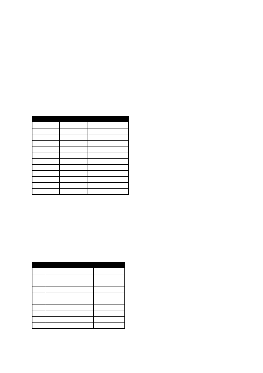
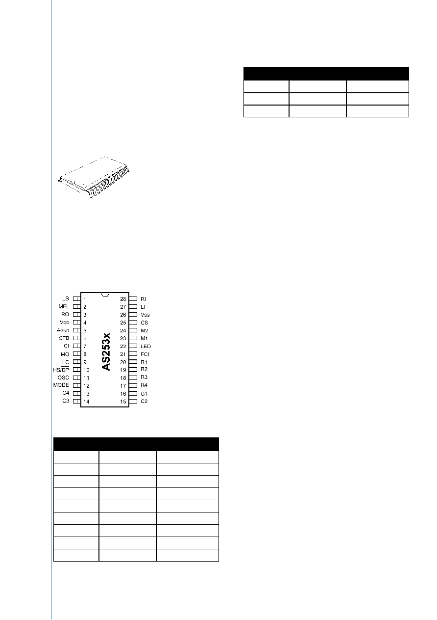
Pin Description
Pin #
Symbol
Function
4
V
DD
Positive Voltage Supply
This is the supply pin for the circuit.
5
A
GND
A
nalog
G
round
This is the analogue ground for the amplifiers.
6
STB
S
ide
T
one
B
alance Input
This is the input for side tone cancellation.
7
CI
C
omplex
I
mpedance Pin
For complex impedance a capacitor should be connected to
8
MO
M
elody
O
utput
PDM output of the melody generator for tone ringing with internal open-drain transistor.
Hi-Z when not active.
9
LLC
L
ine
L
oss
C
ompensation
Select pin for line loss compensation (see also Figure 6 and Figure 7).
LLC = A
GND
: 20 - 50 mA LLC = V
DD
: 45 - 75 mA LLC = V
SS
: none.
10
HS/DP
H
ook
S
witch Input and
D
ial
P
ulse Output
This is an I/O that is pulled high by the hook switch when off-hook and an open drain pulls it low
during break periods of pulse dialing and flash.
11
OSC
OSC
illator Input
Pin for ceramic resonator (3.58 MHz).
Reference:
Murata CSTCC3M58GD3346-R0
SMD
Murata CSTLS3M58GD3458-B0
Lead
12
MODE
Signaling
MODE
Select Input
Mode pin
Function
Open
Dialing inhibited
Row 1
LD mode, 10 pps, 33/66 ms
Row 2
LD mode, 10 pps, 40/60 ms
Row 3
LD mode, 20 pps, 33/66 ms
Row 4
LD mode, 20 pps, 40/60 ms
Row 5
LD mode, 10 pps, 33/66 ms, Temp. MF with tone on first * key entry
Row 61
MF only, 82/82 ms
Row 7
MF only, 82/160 ms
During temporary MF: 82/160 ms
13
14
15
16
C4
C3
C2
C1
Keyboard Columns
(see key arrangements in Figure 2, Figure 3 and Figure 4)
Data Sheet AS2533-36
austria
micro
systems
Revision 8.1
Page 3 of 24
Pin #
Symbol
Function
17
18
19
20
R4
R3
R2
R1
Keyboard Rows
(see key arrangements in Figure 2, Figure 3 and Figure 4)
21
FCI
F
requency
C
omparator
I
nput
This is a Schmitt trigger input for ring frequency discrimination. Disabled during off-hook.
22
LED
LED
Output Driver
Output for driving an LED that will be flashing when in Program/Mute state.
23
24
M1
M2
Microphone Inputs
Differential inputs for the microphone (electret).
25
CS
C
urrent
S
hunt Control Output
This N-channel open drain output controls the external high power shunt transistor for the modulation
of the line voltage and for shorting the line during make period of pulse dialing.
26
V
SS
Negative Power Supply
27
LI
L
ine
I
nput
This input is used for power extraction and line current sensing.
28
RI
R
eceive
I
nput
This is the input for the receive signal.
1
LS
L
ine Current
S
ense Input
This is the input for sensing the line current.
2
MFL
MF
L
evel Setting
A voltage divider connected from this pin to A
GND
and V
SS
can be used to set the DTMF level.
3
RO
R
eceive
O
utput
This is the output for driving a dynamic earpiece with an impedance of 150 to 300
.
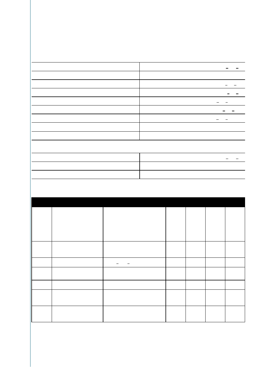
Selection Overview
Function
AS2533
AS 2534B
AS2535
AS2536
Direct memories (one-key)
4
0
12
4
Indirect memories (two-key)
10
0
0
10
Repeat dialing
yes
yes
no
yes
LNR key
yes
yes
yes
yes
Pause insertion by LNR key
yes
yes
yes
yes
Pause (PS) key
yes
yes
no
yes
P/M or MT key
P/M
P/M
P/M
P/M
Tone/Pulse (T/P) key
yes
yes
no
yes
Temporary MF by * key
yes
yes
yes
yes
Centrex (A - D) keys
yes
yes
no
yes
Volume (VOL, ≠/+) keys
yes
yes
yes
yes
Volume reset by off-hook
yes
no
yes
no
Programming of tone ringer
yes
yes
yes
yes
R3 Flash duration
600 ms
600 ms
600 ms
600 ms
Data Sheet AS2533-36
austria
micro
systems
Revision 8.1
Page 4 of 24
Functional Description
Keyboard Connections
(Either VOL or +/≠ keys)
Key closure, R
ON
max. = 1 k
Key open, R
OFF
min. = 1 M
Figure 2 Keyboard Connection AS2533/36
Figure 3 Keyboard Connection AS2534
P
P
P
/
/
/
M
M
M
1
1
1
2
2
2
3
3
3
4
4
4
5
5
5
6
6
6
7
7
7
M
M
M
2
2
2
M
M
M
3
3
3
M
M
M
4
4
4
M
M
M
R
R
R
R
R
R
P
P
P
P
P
P
S
S
S
T
T
T
/
/
/
P
P
P
M
M
M
1
1
1
A
A
A
B
B
B
C
C
C
D
D
D
8
8
8
9
9
9
0
0
0
*
*
*
#
#
#
R
R
R
1
1
1
R
R
R
2
2
2
R
R
R
3
3
3
L
L
L
N
N
N
R
R
R
V
V
V
O
O
O
L
L
L
+
+
+
-
-
-
-
-
-
-
-
-
-
-
-
R1
R2
R3
R4
C1
C2
C3
C4
P
P
P
/
/
/
M
M
M
1
1
1
2
2
2
3
3
3
4
4
4
5
5
5
6
6
6
7
7
7
R
R
R
P
P
P
P
P
P
S
S
S
T
T
T
/
/
/
P
P
P
A
A
A
B
B
B
C
C
C
D
D
D
8
8
8
9
9
9
0
0
0
*
*
*
#
#
#
R
R
R
1
1
1
R
R
R
2
2
2
R
R
R
3
3
3
L
L
L
N
N
N
R
R
R
V
V
V
O
O
O
L
L
L
+
+
+
-
-
-
-
-
-
-
-
-
-
-
-
R1
R2
R3
R4
C1
C2
C3
C4
Data Sheet AS2533-36
austria
micro
systems
Revision 8.1
Page 5 of 24
Keyboard Connections continued
(either VOL or +/≠ keys)
Figure 4 Keyboard Connection AS2535
Power On Reset
The on chip power on reset circuit monitors the supply
voltage (V
DD
) during off-hook. When V
DD
rises above
approx. 1.2V, a power on reset occurs which clears the
RAM.
DC Conditions
The normal operating range is from 13 mA to 100 mA.
Operating range with reduced performance is from 5 mA to
13 mA (parallel operation). In the operating range all
functions are operational.
At line currents below 13 mA the AS253x provides an
additional slope below 4.5V in order to allow parallel
operation (see Figure 12).
The dc characteristic (excluding diode bridge) is
determined by the voltage at LI and the resistor R1 at line
currents above 13 mA as follows:
VLS = VLI + ILINE ◊ R1
The voltage at LI is 4.5V in the normal operating range.
During pulse dialing the speech circuit and other part of
the device not operating is in a power down mode to save
current. The CS pin is pulled to V
SS
in order to turn the
external shunt transistor on to keep a low voltage drop at
the LS pin during make periods.
AC Impedance
The ac impedance of the circuit is set by external
components. The impedance can be real or complex.
The ac impedance is determined as follows:
ZAC = 33 ∑ Z1
The dc value of Z1 should be 30
to maintain correct dc
performance.
Return loss and side tone cancellation can be determined
independent of each other.
Speech Circuit
The speech circuit consists of a transmit and a receive
path with dual soft clipping, mute, line loss compensation
and sidetone cancellation.
P
P
P
/
/
/
M
M
M
1
1
1
2
2
2
3
3
3
4
4
4
5
5
5
6
6
6
7
7
7
M
M
M
9
9
9
M
M
M
1
1
1
0
0
0
M
M
M
1
1
1
1
1
1
M
M
M
1
1
1
2
2
2
M
M
M
5
5
5
M
M
M
6
6
6
M
M
M
7
7
7
M
M
M
8
8
8
M
M
M
1
1
1
M
M
M
2
2
2
M
M
M
3
3
3
M
M
M
4
4
4
8
8
8
9
9
9
0
0
0
*
*
*
#
#
#
R
R
R
1
1
1
R
R
R
2
2
2
R
R
R
3
3
3
L
L
L
N
N
N
R
R
R
V
V
V
O
O
O
L
L
L
+
+
+
-
-
-
-
-
-
-
-
-
-
-
-
R1
R2
R3
R4
C1
C2
C3
C4

Data Sheet AS2533-36
austria
micro
systems
Revision 8.1
Page 6 of 24
Transmit
The gain of the transmit path is 37 dB for 600
line
termination from M1/M2 to LS (see test circuit Figure 9).
The microphone input is differential with an input
impedance of 20 k
.
The soft clip circuit limits the output voltage at LI to 2V
PEAK
(see Figure 11). The attack time is 30
µ
s/6 dB and the
decay time is 20 ms/6 dB. When mute is active, during
dialing or after pressing the P/M key, the gain reduced by >
60 dB.
Receive
The gain of the receive path is 3 dB for 600
line
termination (test circuit Figure 9). The receive input the
differential signal of RI and STB. When mute is active
during dialing the gain is reduced by > 60 dB. During
DTMF dialing a MF comfort tone is applied to the receiver.
The comfort tone is the DTMF signal with level that is -30
dB relative to the line signal.
The receive gain can be changed by pressing the volume
keys. The VOL key gives a +5.4 dB boost and has a toggle
function, i.e. repressing the key resets the gain to default.
As an alternative the +/≠ keys can be used. The + key
increases the gain by 8.1 dB in 3 steps and the ≠ key
decreases the gain by 5.4 dB in 2 steps (total range 13.5
dB). On AS2533/5 the volume is reset to default by next
off-hook and on AS2534/6 the volume setting will remain at
last setting. A POR will always reset the volume to default.
The soft clip circuit limits the voltage at the receive output
(RO) to 1V
PEAK
(see Figure 10). It prevents harsh
distortion and acoustic shock.
Sidetone
A good sidetone cancellation is achieved by using the
following equation:
1
2
Z
Z
Z
Z
BAL
Line
=
The sidetone cancellation signal is applied to the STB
input.
Line Loss Compensation
The line loss compensation is a pin option. When it is
activated, the transmit and receive gains are decreased by
6 dB at line currents from 20 to 50 mA when LLC = A
GND
and 45 to 75 mA when LLC = high (@ R1 = 30
). The line
loss compensation is disabled when LLC = low (see Figure
6 and Figure 7).
Dialing Functions
Valid Keys
The key scanning is enabled when HS/DPN is pulled high
and V
DD
is above V
REF
. A valid key is detected from the
keyboard by connecting the appropriate row to the column
(R
ON
< 1 k
). This can be done using an n x m keyboard
matrix with single contacts. Four diodes are used to extend
the number of rows (see keyboard arrangement fig. 2). It is
also possible to connect a microcontroller to the rows and
columns (see application note AN3010).
P/M and MT Key
The P/M key is used to enter the Program/Mute state.
Depressing the P/M key mutes the speech circuit and the
device is in program state. Repressing the P/M key
deactivates the mute and program state (toggle
function).The MT key works in similar way, but has no
program function.
When program/mute is activated, the LED indication is
turned on (flashing: 80 ms 'on' and 1 sec 'off').
Dial Mode Selection
The default mode (LD or MF) can be selected by the mode
pin. When default LD mode is selected, a temporary
change to MF can be invoked by pressing T/P key (not
AS2535) or the * key (when mode pin = row 5, the MF tone
is generated with the first * key entry). The circuit will
revert to LD by repression the T/P key (not AS2535) or by
pressing the R (R1, R2 or R3) key or by next on-hook.
When MF mode is selected by the mode pin, the circuit can
not be changed temporary to LD but will remain in MF
mode.
Centrex Keys (not AS2535)
The alphanumeric keys accommodate easy use of centrex
services. The A, B, C and D keys are only valid in MF
mode (including temporary MF) and are not storable.
Pressing one of these keys will invoke the appropriate
MF tones to be transmitted.
The centrex keys are not stored in the RAM, and
subsequently entered digits are buffered in FIFO.
Z
LI
Z
BA
Z
1
Z
2
Figure 5 Side Tone Balance

Data Sheet AS2533-36
austria
micro
systems
Revision 8.1
Page 7 of 24
Last Number Redial
LNR is a facility that allows resignalling of the last
manually dialed number without keying in all the digits
again. The LNR is repeatable after each off-hook.
The current content of the RAM is overwritten by new
entries.
A manually entered number is automatically stored in the
LNR RAM. The capacity of the RAM is 31 digits. If a
number greater than 31 digits is entered, the LNR facility
will be inhibited (until new entries < 32 digits) and further
entries will be buffered in FIFO.
Pauses can be inserted by pressing the PS key (not
AS2535).
Post dialed digits, i.e. digits manually entered after LNR
has been invoked, are not stored in RAM but buffered in
FIFO.
Repeat Dialing (not AS2535)
The last manually dialed number can be repeated without
going on-hook by pressing the RP key. If a called number
is engaged, pressing the RP key will break the line for 1.6
second (to get a new dial tone) and after a pause the
number will be repeated.
The repeat function is enabled when prior to pressing the
RP key, a number has been dialed, and it can be invoked
an unlimited number of times until next on-hook. During the
1.6 second break the device is in power down mode to
save current.
Recall Function
A recall (R1, R2 or R3 key) activation will invoke a flash
(timed loop break), however, the R1 flash is never
executed in LD mode. R2 and R3 will be executed
independent of the mode.
If recall is the first entry in a digit string, it will be stored in
LNR RAM when digit(s) are entered after the recall.
If the recall key is depressed after a digit string has been
entered or dialed out, the recall will not be stored but
buffered in the FIFO together with subsequently entered
digit.
If pressing the recall key is not followed by digit entries,
the LNR RAM remains intact.
After a recall a 270 ms pause will automatically be
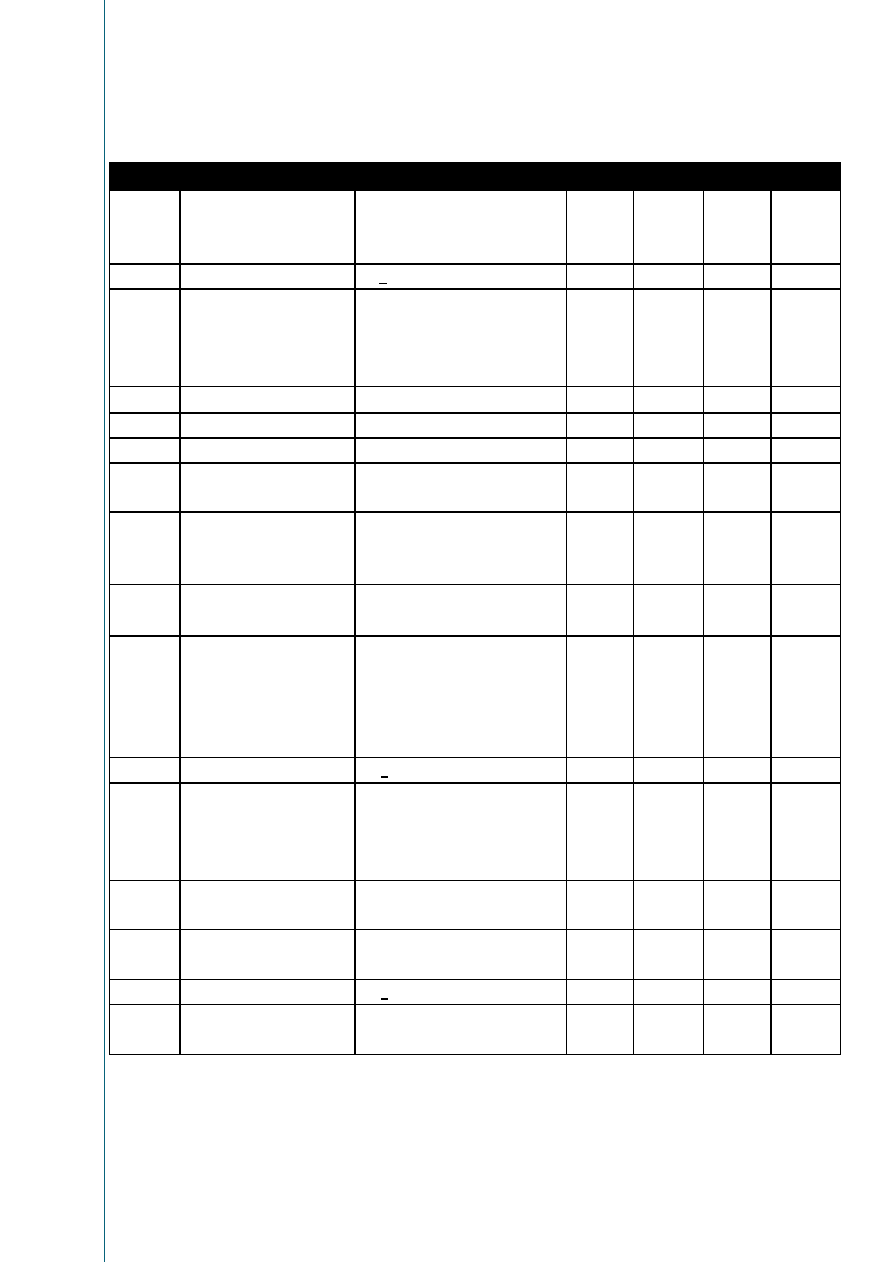
Memory Keys (not AS2534)
The keys M1 to M12 are direct memory access keys and
the MR key (AS2533/6 only) is used for abbreviated
dialing.
Memory arrangement
AS2533/6
AS2534
AS2535
Storable numbers
14
0
12
Direct memory keys
4
0
12
Indirect memories
10
0
0
In the on chip RAM, numbers can be stored. Each number
can contain up to 21 digits (including pauses).
During programming multiple pauses can be inserted by
pressing the PS (not AS2535) or the LNR key. Each pause
inserted within the first 5 entries will automatically be
terminated after 2 seconds whereas pauses inserted after
location 5 in a digit string will halt dialing and can be
terminated manually by pressing the PS (not AS2535) or
the LNR key. The halt function allows in-dialing to an
extension on a PABX.
Example (45678≠123 is stored in M1, where ≠ is a
pause/wait and 123 the extension number):
off-hook, wait for dial tone
press M1 (45678 is dialed out)
await dial tone from called PABX
press PS or LNR (123 is dialed out)
Memory dialing is cascadable. However, the content of one
memory must be dialed out before a new can be invoked.
Sliding Cursor Procedure
To accommodate easy and uncomplicated redialing (LNR)
behind a PABX, a sliding cursor protocol is implemented. If
new entries match the previous RAM contents, pressing
the LNR key will dial out the remaining digits.
If there is an error in matching, the LNR will be inhibited
until next on-hook, and the RAM will contain the new
number.
Example (LNR content 912345, where 9 is access code):
off-hook, wait for PABX dial tone
press 9 and wait for external dial tone
press LNR (12345 will be dialed out).
Tone Generator
The tone generator incorporates the DTMF tones, 3 basic
frequencies for the tone ringer and pacifier tones.
DTMF
The DTMF generator provides 8 frequencies, namely:
Data Sheet AS2533-36
austria
micro
systems
Revision 8.1
Page 8 of 24
Low group
Digit 1-2-3-A
697 Hz
Digit 4-5-6-B
770 Hz
Digit 7-8-9-C
852 Hz
Digit * -0-# -D
941 Hz
High group
Digit 1-4-7- *
1209 Hz
Digit 2-5-8-0
1336 Hz
Digit 3-6-9-#
1477 Hz
Digit A-B-C-D
1633 Hz (not AS2535)
The MF output level can be set with an external voltage
divider on pin MFL.
Voltage at pin MFL (2)
DTMF Level
(Low Grp.)
A
GND
typ. 1.50* V
-4.0 dBm
0.878 * A
GND
1.317 V
-5.2 dBm
0.791 * A
GND
1.187 V
-6.4 dBm
0.705 * A
GND
1.058 V
-7.6 dBm
0.620 * A
GND
0.930 V
-8.8 dBm
0.495 * A
GND
0.743 V
-10.0 dBm
0.372 * A
GND
0.558 V
-11.2 dBm
0.290 * A
GND
0.435 V
-12.4 dBm
0.210 * A
GND
0.315 V
-13.6 dBm
0.130 * A
GND
0.195 V
-14.8 dBm
V
SS
0.000 V (V
SS
)
-16.0 dBm
(Z
LINE
= 600)
*typical MFL values for A
GND
= 1.5V
The preemphasis is 2.6 dB.
The MF tones are according to CEPT recommendations.
Tone Ringer (Melody/Volume)
The three basic frequencies of the melodies are:
F1 = 800 Hz, F2 = 1067 Hz, and F3 = 1333 Hz (± 5%).
The repetition rate and the volume of the tone ringer
melodies can be programmed by pressing P/M and #
followed by a digit as follows:
Digit
Repetition Rate
Volume
1
1 time (50 ms pause)
- 16 dB
2
1 time (50 ms pause)
- 7 dB
3
1 time (50 ms pause)
0 dB (max.)
4
4 times
- 16 dB
5
4 times
- 7 dB
6
4 times (default)
0 dB (max.)
7
10 times
- 16 dB
8
10 times
- 7 dB
9
10 times
0 dB (max.)
0
None
Off
The procedure is ended by repressing the P/M key.
The default setting is digit 6, i.e. after a power on reset the
device will start up with repetition rate 4 and maximum
volume. If digit 0 is programmed, the tone ringer will be
turned off until next off-hook where it will turn back to the
last setting before 0. The programmed settings are stored
in the on chip RAM.
Repetition rate means that a sequence of 6 frequencies
is repeated 1, 4 or 10 times within 1 second.
The sequence of the frequencies is controlled by the
sequence register as follows:
Sequence F1 F2 F3 F1 F2 F3 ...
Pacifier Tone
By MF dialing the DTMF tones are provided to the earpiece
as comfort tone.
During programming a key entry is acknowledged by a
pacifier tone of 1477 Hz. The level of the pacifier tone is
approximately 60 mV at the RO output. The duration is 40
ms after every key entry in program mode.
When terminating the program mode with the P/M key an
acknowledge tone of 140 ms is provided. An invalid key
entry, however, will cause a termination of the program
mode indicated by a rejection tone of 4 times 40 ms with
28 ms pauses between the tone bursts.
Ring Frequency Discrimination
The ring frequency discriminator assures that only signals
with a frequency between 13Hz and 70 Hz are regarded as
valid ring signals. The time for recognizing a valid ring
signal is 1/f seconds, where 'f' is the ring frequency.
When a valid ring signal is present for 73 ms continuously,
the melody generator is activated and remains active as
long as the ring signal is present.
Once the melody generator has been started, the ring
signal is continuously monitored and the melody generator
is instantly turned on or off according to the momentary
presence of a valid or invalid ring signal respectively (until
next POR or off-hook).

Data Sheet AS2533-36
austria
micro
systems
Revision 8.1
Page 9 of 24
Typical Characteristics of
Line Loss Compensation
Figure 6 Typical Tx Gain Characteristics Line Loss Compensation
Figure 7 Typical Rx Gain Characteristics Line Loss Compensation
f = 800 Hz
Z
LINE
= 600
V
LS
= -10 dBm
20
30
40
50
60
70
80
(mA)
DC Line
Current
LLC = V
SS
LLC = V
DD
LLC = A
GND
Tx Gain
(dB)
29
30
31
32
33
34
35
f = 800 Hz
Z
LINE
= 600
V
LS
= -10 dBm
VOL = 0 dB (neutral)
20
30
40
50
60
70
80
(mA)
DC Line
Current
LLC = V
SS
LLC = V
DD
LLC = A
GND
Rx Gain
(dB)
-2
-1
0
+1
+2
+3
+4

Data Sheet AS2533-36
austria
micro
systems
Revision 8.1
Page 10 of 24
Typical Application
Complex Impedance
(270 W + 750 W // 150 nF)
Only the components
necessary for
presenting the
complete functions of
the AS253x are
included.
The external components
might change to comply
with various national PTT
regulations and to interface
to different transducers.
Since the AS253x is a
component and not a complete
system, it can not be approved
as a stand alone part by the
standard bodies. Hence, full
conformance to any standards
is depending on the application
in which the AS253x is being
used, and therefore, approvals
by the standard bodies are the
responsibility of the customer
and austriamicrosystems AG will
not have tested the product to
meet specific standards.
For further application
information please refer to
application note AN2201
.
Figure 8 Typical Application

Data Sheet AS2533-36
austria
micro
systems
Revision 8.1
Page 11 of 24
Programming Procedures
Procedure Principles
The procedures for utilizing the features of the AS253x are
optimized out of consideration for the human factor in
order to:
-
meet the user's expectations
-
be easy to learn and relearn
-
not invoke any automatic functions which the user
doesn't expect
-
protect the user from committing critical errors, e.g.
dialing wrong numbers, deleting stored numbers, etc.
-
be consistent, simple and usable.
The following chapters describe the operating procedures
for the provided features. Pressing an invalid key or key
combination during programming will cause the device to
abort the program state. Pressing any key combination or
sequence which is not described or defined may cause the
device to enter a state or mode that does not comply with
the expectation of the user. In such cases, any undesired
state can be terminated at any time by going on-hook / off-
hook which will generate a functional reset.
Storing Numbers (not AS2534)
Up to 12 numbers, each with maximum 24 digits, can be
stored into the internal RAM.
1. Press [P/M] to enter program mode
2. Enter location (MR + digit
1
; or M1 to M12)
3. Enter number - entries (0-9, *, #, PS or LNR, R1, R2,
R3) will b written directly into the selected memory
location)
4. Press [P/M] to store and exit or go on-hook to abort
5. Go to 1 for storing further numbers
Programming Tone Ringer
Three different ringer melodies with three levels each can
be programmed.
1. Press [P/M] to enter program mode
2. Press [#] for ringer programming mode
3. Enter Code to select ringer melody and volume(see
code table in section Tone Ringer (Melody/Volume)
4. Press [P/M] to store and exit or go on-hook to abort
1
Digit includes 0 ≠ 9,
and #
When Code 0 (tone ringer off) has been programmed, the
device will automatically return to previous setting
(different from 0) by next off-hook.
Temporary MF
The procedure below assumes that the device is operated
in puls mode.
1. Go off-hook
2. Press [*] or [T/P] to switch to DTMF mode
3. Press [R] or [T/P] to switch back to PULS mode
4. Got to 1 to switch again to DTMF mode
Mode pin is connected to row 1, 2, 3, 4, or 5. When mode
pin = row 5, pressing the [*] key also transmits the tone by
MF selected. The [T/P] key (not AS2535) can be used
alternatively to the [*] key.
Automatic Dialing
The following procedure describes the dialing procedure
and the internal sequences:
1. Go off-hook
2. Enter the number by pressing digit, [M1]-[M12], [LNR]
or [MR] + digit
3. The number is internally buffed in the FIFO
4. Tone- or Puls-Dialing starts
5. Wait for connection
6. Got to 2 for entering postdialed digits
Postdialed digits are not stored but buffed in the FIFO.

Data Sheet AS2533-36
austria
micro
systems
Revision 8.1
Page 12 of 24
Timing Diagrams
LD Dialing
LD Dialing with Access Pause
MF Dialing
t
IDP
t
B
t
PDP
t
IDP
t
PDP
t
M
t
M
t
B
t
M
t
B
MUTE
MASK
HS/DPN
t
PDP
t
PDP
t
M
t
M
t
M
t
IDP
t
B
t
IDP
t
B
t
B
MUTE
MASK
HS/DPN
t
AP
t
TD
t
ITP
MUTE
HS/DPN
LS
t
TD
t
TD
t
ITP
t
ITP
t
AP

Data Sheet AS2533-36
austria
micro
systems
Revision 8.1
Page 13 of 24
Flash
Repeat Dialing (not AS2535)
t
AP
MUTE
HS/DPN
Power Down
t
RP
Number
engaged
New
connection
RP key
DIALLING
t
FD
t
M
t
M
t
M
t
FD
t
M
MUTE
MASK
HS/DPN
t
PFP
Data Sheet AS2533-36
austria
micro
systems
Revision 8.1
Page 14 of 24
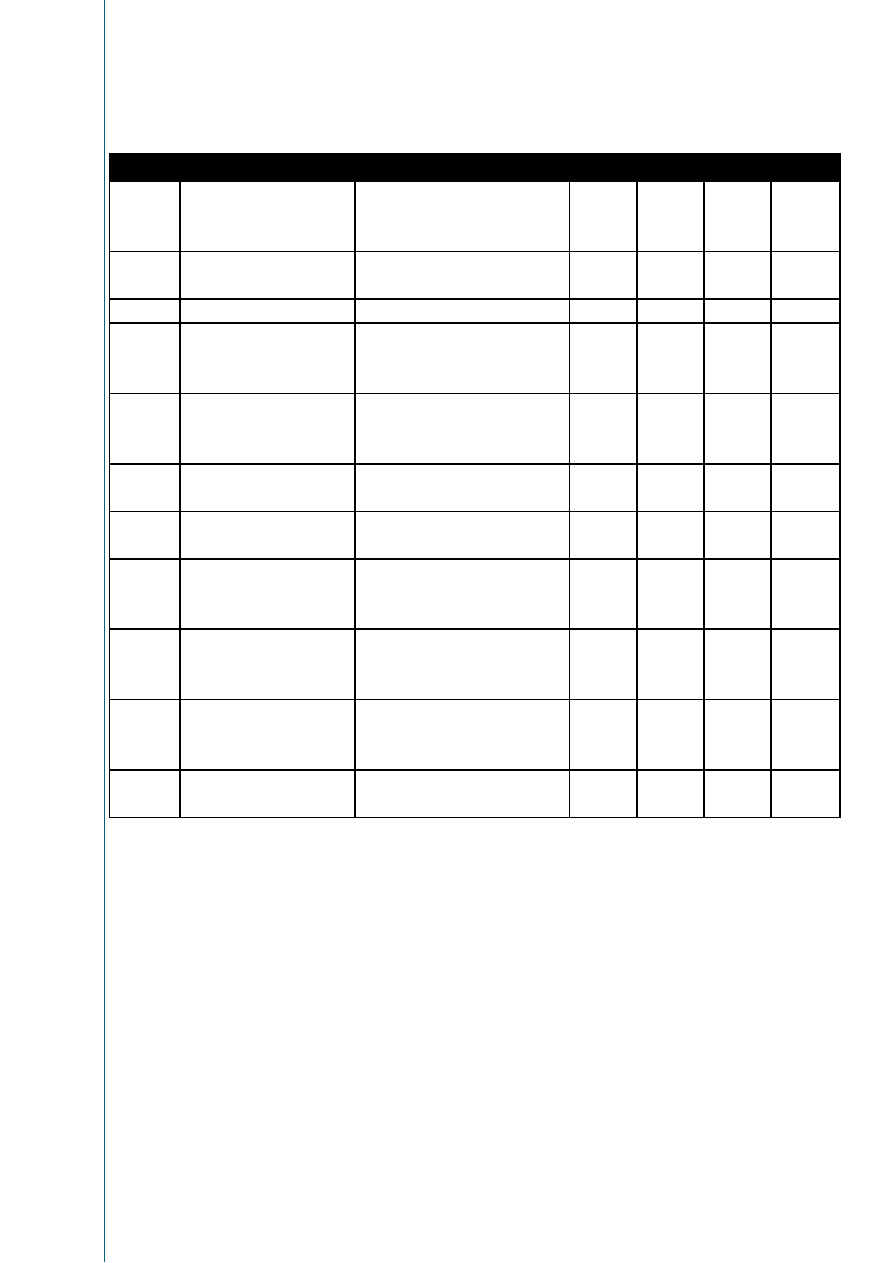
Electrical Characteristics
Absolute maximum ratings
Positive Supply Voltage
-0.3V < V
DD
< 7V
Input Current
± 25mA
Input Voltage (LS)
-0.3V < V
IN
< 10V
Input Voltage (LI, CS)
-0.3V < V
IN
< 8V
Input Voltage (STB, RI)
-2V < V
IN
< V
DD
+0.3V
Input Voltage (MO)
-0.3V < V
IN
< +35V
Digital Input Voltage
-0.3V < V
IN
< V
DD
+0.3V
Electrostatic Discharge (HBM 1.5k
-100pF)
± 1000V
Storage Temperature
-65∞C to +125∞C
Recommended operating conditions
Supply Voltage * (Speech Mode)
3.8V < V
DD
< 5V
Oscillator Frequency (Resonator: Murata CSA 3.58M G312AM)
3.58 MHz
Operating Temperature
-25∞C to +70∞C
*
This voltage is generated internally
DC Characteristics
(I
LINE
= 15 mA unless otherwise specified)
Symbol
Parameter
Conditions
Min.
Typ.
Max.
Units
I
DD
Operating Current
Speech mode
MF dialing
LD dialing, V
DD
= 2.5V
Ring mode, V
DD
= 2.5V
3
4
200
300
5
mA
mA
µA
µA
I
DD0
Retention Current
Idle mode, V
DD
= 2 V,
T
AMB
= 25∞C
0.05
µA
V
LI
Line Voltage (default)
13 mA < I
LINE
< 100 mA
4.5
V
I
OL
Output Current, Sink
CS, HS/DP, MO
V
OL
= 0.4V
1.5
mA
I
OL
Output Current, Sink; LED
V
OL
= 0.4V
4
mA
V
IL
Input Low Voltage
HS/DPN; FCI
T
AMB
= 25∞C
V
SS
0.3 V
DD
V
V
IH
Input High Voltage
HS/DPN; FCI
T
AMB
= 25∞C
0.7 V
DD
V
DD
V
Data Sheet AS2533-36
austria
micro
systems
Revision 8.1
Page 15 of 24
AC Characteristics
(I LINE = 15 mA; f = 800 Hz unless otherwise specified)
Symbol
Parameter
Conditions
Min
Typ
Max
Units
Tx
Transmit
Test Circuit Figure 9
A
TX
Gain, Transmit
M1/M2 to LI
35.1
36.6
38.1
dB
A
TX/F
Variation with Frequency
f = 500 Hz to 3.4 kHz
±0.8
dB
THD
Distortion
V
LI
< 0.25V
RMS
2
%
V
AGC
Soft Clip Level
2
V
PEAK
A
SCO
Soft Clip Overdrive
20
dB
t
ATTACK
Attack Time
30
µ
s/6 dB
t
DECAY
Decay Time
20
ms/6dB
Z
IN
Input Impedance (M1/M2)
20
k
A
MUTE
Mute Attenuation
Mute activated
60
dB
V
NO
Noise Output Voltage
T
AMB
= 25∞C
-72
dBmp
V
IN Max
Input Voltage Range
Differential
±1
V
PEAK
(M1/M2)
Single Ended
±0.5
V
PEAK
BJT
Output Driver
V
IN MAX
Input Voltage Range (LI)
±2
V
PEAK
V
TX
Dynamic Range
±2
V
PEAK
RL
Return Loss
Z
RL
=1000
; T
AMB
= 25∞C
18
dB
Z
AC/TEMP
Temperature Variation
0.5
/∞C
Rx
Receive
Test Circuit Figure 9
A
RX
Receive Gain (Vol. default)
LI to RO
1.5
3
4.5
dB
A
VOL
Volume Gain
VOL key
+5.4
dBr
A
VOL
Volume Gain
≠/+ keys
-5.4/+8.1
dBr
A
RX/F
Variation with Frequency
f = 500 Hz to 3.4 kHz
±0.8
dB
THD
Distortion
V
RI
< 0.25V
RMS
2
%
V
AGC
Soft Clip Level
V
RO
=
1
V
PEAK
A
SCO
Soft Clip Overdrive
10
dB
t
ATTACT
Attack Time
V
RI
> 0.8V
RMS
30
µ
s/6 dB
t
DECAY
Decay Time
20
ms/6dB
V
NO
Noise Output Voltage
T
AMB
= 25∞C
-72
dBmp
V
UFC
Unwanted F. Components
50 Hz....20 kHz
-60
dBm
Z
IN
Input Impedance (RI)
8
k
V
IN RI
Input Voltage Range (RI)
±2
V
PEAK
A
ST
Sidetone Cancellation
V
RI
< 0.25V
RMS
26
dB
V
IN ST
Input Voltage Range (STB)
±2
V
PEAK
Z
IN
Input Impedance (STB)
80
k

Data Sheet AS2533-36
austria
micro
systems
Revision 8.1
Page 16 of 24
AC Characteristics (cont¥d)
(I
LINE
= 15 mA; f = 800 Hz unless otherwise specified
)
Symbol
Parameter
Conditions
Min
Typ
Max
Units
Keyboard
t
D
Key Debounce Time
15
ms
HS/DPN Input
t
HS-L
Low to High Debounce
Going off-hook
15
ms
t
HS-H
High to Low Debounce
Not LD dialing
210
ms
During LD dialing
270
ms
DTMF
F
Frequency deviation
T
AMB
= 25∞C, Note 5
1.2
%
V
MF
MF Tone Level (Low group)
MFL = A
GND
,
T
AMB
= 25∞C
- 2.5
- 4
- 5.5
dB
V
MF
MF Tone Level (Low group)
MFL Range = V
SS
... A
GND
,
T
AMB
= 25∞C
-16...-4
dB
V
L-H
Preemphasis Low to High
T
AMB
= 25∞C,
1.8
2.4
3.0
dB
V
UFC
Unwanted F. Components
300 Hz...5 kHz
- 40
dBm
Note 3; MFL = V
SS
5 kHz...14 kHz
- 50
dBm
14 kHz...28.5 kHz
- 70
dBm
28.5 kHz...40 kHz
- 80
dBm
t
TD
Tone Duration
Note 1&6; Mode=row 6 or 7
80
82.3
85
ms
t
ITP
Inter Tone Pause
Note1; Mode=row 6
80
82.3
85
ms
t
ITP
Inter Tone Pause
Note 1 & 6; Mode=row 7
150
165
170
ms
t
TR
Tone Rise Time
Note 2
5
ms
t
TF
Tone Fall Time
Note 2
5
ms
LD
t
DR
Dial Rate
Mode = row 1, 2 or 5
9.53
10
10.5
pps
Mode = row 3 or 4
19.05
20
21
pps
t
/B
Break Period
Mode = row 2
57
61.2
63
ms
t
/B
Break Period
Mode = row 4
28.5
30.6
31.5
ms
t
/B
Break Period
Mode = row 1 or 5
63
66
69
ms
t
/B
Break Period
Mode = row 3
31.5
33
34.5
ms
t
M/
Make Period
Mode = row 2
38
40.8
42
ms
t
M/
Make Period
Mode = row 4
19
20.4
21
ms
t
M/
Make Period
Mode = row 1 or 5
31.5
33
34.5
ms
t
M/
Make Period
Mode = row 3
15.7
16.5
17.3
ms
t
PDP
Pre-Digit Pause
35
ms
t
IDP
Inter Digit Pause
Mode = row 1, 2, 3, 4 or 5
800
840
880
ms
t
HS-H
High to Low Debounce
During LD dialing
270
ms
t
MO
Mute Overhang
t
M
Data Sheet AS2533-36
austria
micro
systems
Revision 8.1
Page 17 of 24
Symbol Parameter
Conditions
Min
Typ
Max
Units
t
FD
Flash Duration 1
R1 key
100
102
ms
Flash Duration 2
R2 key
270
300
ms
Flash Duration 3
R3 key (AS2533/4B/5/6)
600
650
ms
t
PFP
Post Flash Pause
274
ms
t
AP
Access Pause
Note 8
2.0
2.05
2.12
sec
t
RP
Repeat Break Time
1.6
sec
Tone Ringer
V
MO
Melody Output
PDM
t
MD
Melody Delay
10
ms
F1
Frequency 1
800
Hz
F2
Frequency 2
1067
Hz
F3
Frequency 3
1333
Hz
t
DT
Detection Time
Initial
1/f + 73ms
s
t
TO
Detection Time-out
note 4
ms
f
MIN
Min. Detection Frequency
13
Hz
f
MAX
Max. Detection Frequency
70
Hz
Pacifier Tone
Program Mode Only
f
PT
Frequency
P/M mode, key entry
1477
Hz
V
RT
Level (RO)
Key entry
60
mV
t
RTD-E
Duration, Key Entry
Valid key entry, prog.
40
ms
t
RTD-A
Duration, Acknowledge
Terminate with P/M key
140
ms
t
RTD-R
Duration, Reject
Invalid key entry, note 7
4x40
ms
LED Output
t
LED-ON
"on-time"
P/M state
80
ms
t
LED-OFF
Interval
P/M state
1
sec
Comfort Tone (DTMF)
V
CT
Level (RO)
Relative to LS
-30
dBr
Note 1: The values are valid during automatic dialing and
are minimum values during manual dialing, i.e. the
tones will continue as long as the key is depressed.
Note 2: The rise time is the time from 10% of final value till
the tone amplitude has reached 90 % of its final
value.
Note 3: Relative to high group.
Note 4: The FCI circuit is reset by POR and HS/DPN pulled
high (off-hook). After a reset the FCI circuit is in a
standby state. A positive edge on FCI will start a 73
ms timer and the frequency discrimination is
initiated. Whenever a period of the ring signal is
missing, the timer is reset. When a valid ring signal
is present for 73 ms, the melody generator is
started and is directly controlled by the ring signal.
This condition will remain until a new reset.
Note 5: This does not include the frequency deviation of the
ceramic resonator.
Note 6: During temporary MF mode.
Note 7: An invalid key entry in program mode will invoke a
tone sequence with 4 tone bursts of 40 ms and
pauses between bursts of 28 ms and abort the
program mode.
Note 8: Pauses inserted within the first 5 entries of a digit
string will be automatically terminated after 2
seconds. Pauses inserted after location 5 can only
be terminated manually by pressing the PS or LNR
key.

Data Sheet AS2533-36
austria
micro
systems
Revision 8.1
Page 18 of 24
Test Circuit
Figure 9 Test Circuit

Data Sheet AS2533-36
austria
micro
systems
Revision 8.1
Page 19 of 24
Characteristic Curves (Typical)
0
1
2
3
4
5
6
7
8
0
10
20
30
40
50
60
70
80
90
100
Line Current [mA]
DC Mask [
V
]
VLI
VLS
Typically
No AC signals
Tamb: 25∞C
Figure 12 DC Mask
Figure 10 Receive Soft Clipping and Distortion
Figure 11 Transmit Soft Clipping and Distortion
0,0
0,2
0,4
0,6
0,8
1,0
1,2
0,00
0,25
0,50
0,75
1,00
1,25
1,50
1,75
2,00
Line Input Voltage (LS)
Receive Output Voltage (RO)
0
1
2
3
4
5
6
7
8
9
10
11
12
D
i
st
ort
i
on
[Vp]
[Vp]
VRO
THD
Line Current: 20mA
Frequency: 800Hz
Tamb: 25∞C
Typically
soft clipping
[%]
0,0
0,5
1,0
1,5
2,0
2,5
0
25
50
75
100
125
150
Microphone Input Voltage (M1/M2)
Line Output Voltage (LS)
0
1
2
3
4
5
6
7
8
9
10
Di
st
or
t
i
on
[Vp]
[mVp]
VLS
THD
Line Current: 20mA
Frequency: 800Hz
Tamb: 25∞C
Typically
soft clipping
[%]

Data Sheet AS2533-36
austria
micro
systems
Revision 8.1
Page 20 of 24
Bond Pad Layout
Sizes and Coordinates
Die Size:
3.190mm x 2.975mm
Bond Pad Size:
85µm x 85µm
Bond Pad Co-ordinates:
Reference co-ordinate of DIE = DIE center
Reference co-ordinate of PAD = PAD center
x
[µm]
y
[µm]
Pad Name
Pin No
x
[µm]
y
[µm]
Pad Name
Pin No
Pads on the Left
Pads on the Right
-1413.50
1052.25
VDD
4
1392.50
-1053.80
R1
20
-1413.50
796.25
AGND
5
1392.50
-663.00
FCI
21
-1413.50
586.25
STB
6
1392.50
-319.80
LED
22
-1413.50
226.25
CI
7
1413.50
408.75
M1
23
-1399.50
67.90
N.C.
1413.50
683.75
M2
24
-1399.50
-234.10
N.C.
Pads on the Top
-1399.50
-400.30
N.C.
1227.50
1301.25
CS
25
-1392.50
-628.50
MO
8
1079.50
1301.25
VSS
26
-1392.50
-1038.80
LLC
9
969.50
1301.25
VSS
26
Pads on the Bottom
627.50
1301.25
LI
27
-1238.10
-1285.00
HS/DP
10
54.50
1301.25
RI
28
-862.10
-1285.00
OSC
11
-90.50
1301.25
LS
1
-696.70
-1285.00
MODE
12
-449.50
1301.25
MFL
2
-432.50
-1285.00
C4
13
-744.50
1301.25
RO
3
-267.10
-1285.00
C3
14
-2.90
-1285.00
C2
15
379.90
-1285.00
C1
16
677.30
-1285.00
R4
17
842.70
-1285.00
R3
18
1173.30
-1285.00
R2
19

Data Sheet AS2533-36
austria
micro
systems
Revision 8.1
Page 21 of 24
Vertical Structure of Bond Pads
Process CXQ/CXB ≠ FAB B
General Conditions
Passivation
200 nm silicon oxynitride + 550 nm silicon nitride
Marking of Failure Dice
Ink Dots, water resistant, Diameter 0.4...1.2 mm
Allowed Loss after Assembly
< 5% in average
< 10% for a single delivery lot
Compensation is limited to replacement of the number of defectives exceeding the above
allowances.
Quantity of dice per delivery lot Only complete wafers can be delivered, therefore the number of good dice delivered may
differ from the order quantity up to
±
1000 pcs.
Storage Conditions
Dice on wafer or dice on foil must be stored in originally sealed boxes or bags.
For storage period - see below.
Except for RMA, opened boxes or bags will not be accepted by austriamicrosystems for return
Conditions for Delivery as Wafer
Wafer diameter
200 mm
Wafer thickness
380
±
20µm
Back finishing
back grinding, silicon
Scribe lane width
100
±
20µm
Packing
Wafer Box Ultrapack 200 / sealed in foil bags
Max. Storage time in sealed
box
6 month, Tamb = 25
∞
C
Layer Specification
metal 2
upper layer:
lower layer:
960 nm AISiCu
98.5% Aluminium
1.0% Silicon
0.5 % Copper
40 nm Titanium
metal 1
upper layer:
lower layer:
450 nm AISiCu
98.5 % Aluminium
1.0% Silicon
0.5 % Copper
40 nm Titanium
metal 1 barrier
upper layer
lower layer
80nm Titanium Nitride
30nm Titanium
polysilicon
270 nm polysilicon
oxide
460 nm thermal oxide
silicon substrate
polysilicon
Si
substrate
oxide
metal 1 barrier
metal 1
metal 2

Data Sheet AS2533-36
austria
micro
systems
Revision 8.1
Page 22 of 24
Conditions for Delivery as Dice on Foil, sawn
Die thickness
380
±
20µm
Back finishing
back grinding, silicon
Frame
Material: Plastic
Size: see figure
Frame Position Tolerance
Center wafer to frame:
±
4mm
Angle deviation wafer to frame:
±
8
∞
Orientation wafer to frame: Wafer flat to frame side with kerfs
Covering adhesive foil to frame: >5mm
Tape
Type: PVC with acrylic adhesive
Thickness: 70
±
20 µm
Sawing conditions
Sawing mode: Saw - through mode
Sawing width: typ. 60 µm
Kerf depth in foil: typ. 20 µm
XV -dimension deviation: max.25 µm
Packing
frame sealed in foil bags filled with nitrogen
Storage time In sealed bags
2 months, Tamb = 25
∞
C
Mechanical Drawing of Frame
Data Sheet AS2533-36
austria
micro
systems
Revision 8.1
Page 23 of 24
Packaging
The device is available in the packages outlined below (not
to scale). For exact mechanical package dimensions
please see austriamicrosystems
AG
packaging information.
28-pin plastic SOIC (suffix T)
Max. Body Length
18.1mm / 713mil
Max. Body Width
7.6mm / 300mil
Pitch
1.27mm / 50mil
Pin Configuration
28 Pin SOIC (suffix T)
Ordering Information
Device
Package
Memories
AS2533 T
28 pin SOIC
4 direct/10 indirect
AS2533 F
Dice on Foil, sawn 4 direct/10 indirect
AS2533 W
Dice on Wafer
4 direct/10 indirect
AS2534B T
28 pin SOIC
none
AS2534B F
Dice on Foil, sawn none
AS2534B W
Dice on Wafer
none
AS2535 T
28 pin SOIC
12 direct
AS2535 F
Dice on Foil, sawn 12 direct
AS2535 W
Dice on Wafer
12 direct
Device
Package
Memories
AS2536 T
28 pin SOIC
4 direct/10 indirect
AS2536 F
Dice on Foil, sawn 4 direct/10 indirect
AS2536 W
Dice on Wafer
4 direct/10 indirect
Devices sold by austriamicrosystems AG are covered by
the warranty and patent identification provisions appearing
in its Term of Sale. austriamicrosystems AG makes no
warranty, express, statutory, implied, or by description
regarding the information set forth herein or regarding the
freedom of the described devices from patent infringement.
austriamicrosystems AG reserves the right to change
specifications and prices at any time and without notice.
Therefore, prior to designing this product into a system, it
is necessary to check with austriamicrosystems AG for
current information. This product is intended for use in
normal commercial applications. Applications requiring
extended temperature range, unusual environmental
requirements, or high reliability applications, such as
military, medical life-support or life-sustaining equipment
are specifically not recommended without additional
processing by austriamicrosystems AG for each
application.
Copyright
Copyright © 1997-2002, austriamicrosystems AG, Schloss
Premstaetten, 8141 Unterpremstaetten, Austria-Europe.
Trademarks Registered Æ. All rights reserved. The material
herein may not be reproduced, adapted, merged,
translated, stored, or used without the prior written consent
of the copyright owner.
The information furnished here by austriamicrosystems AG
is believed to be correct and accurate. However,
austriamicrosystems AG shall not be liable to recipient or
any third party for any damages, including but not limited
to personal injury, property damage, loss of profits, loss of
use, interruption of business or indirect, special, incidental
or consequential damages, of any kind, in connection with
or arising out of the furnishing, performance or use of the
technical data herein. No obligation or liability to recipient
or any third party shall arise or flow out of
austriamicrosystems AG rendering of technical or other
services.

Data Sheet AS2533-36
austria
micro
systems
Revision 8.1
Page 24 of 24
Contact
Headquarters
austriamicrosystems AG
Communications Business Unit
A 8141 Schloss Premst‰tten, Austria
T. +43 (0) 3136 500 0
F. +43 (0) 3136 525 01
www.austriamicrosystems.com
Sales Offices
Germany
austriamicrosystems Germany GmbH
Tegernseer Landstrasse 85
D-81539 M¸nchen, Germany
Phone: +49/89/693643-0
Fax: +49/89/693643-66
France
austriamicrosystems France S.a.r.l.
124, Avenue de Paris
F-94300 Vincennes, France
Phone: +33/1/43 74 00 90
Fax: +33/1/43 74 20 98
Italy
austriamicrosystems Italy S.r.l.
Via Leone Tolstoi, 64
I-20146 Milano, Italy
Phone: +39/0242/36713
Fax: +39/0242/290889
Switzerland
austriamicrosystems Switzerland AG
Rietstrasse 4
CH-8640 Rapperswil, Switzerland
Phone: +41/55/220 9000
Fax: +41/55/220 9001
USA (west)
austriamicrosystems USA, Inc.
Suite 116, 4030 Moorpark Ave,
San Jose, CA 95117, USA
Phone: +1/408/345 1790
Fax: +1/408/345 1795
USA (east)
austriamicrosystems USA, Inc.
Suite 400, 8601 Six Forks Road
Raleigh, NC 27615, USA
Phone: +1/919/676 5292
Fax: +1/919/676 5305
United Kingdom
austriamicrosystems UK, Ltd.
Coliseum Business Centre, Watchmoor Park
Camberley, Surrey, GU15 3YL, UK
Phone: +44/1276/23 3 99
Fax: +44/1276/29 3 53
Japan
austriamicrosystems AG
Shin Yokohama Daini, Center Bldg. 10F
3-19-5, Shin Yokohama
Kohoku-ku, Yokohama 222-0033, Japan
Phone: +81/45/474 0962
Fax: +81/45/472 9845
Distributors & Representatives
austriamicrosystems AG is represented by distributors in
the following countries. Please contact your nearest
regional sales office for the distributor address:
Spain, Israel, Korea, Hong-Kong, Taiwan, Malaysia,
Singapore, India, Brazil
Application Support
Please contact your local sales office or your distributor.