 | –≠–ª–µ–∫—Ç—Ä–æ–Ω–Ω—ã–π –∫–æ–º–ø–æ–Ω–µ–Ω—Ç: AS2534BT | –°–∫–∞—á–∞—Ç—å:  PDF PDF  ZIP ZIP |

1
Rev. 7
July 1998
Data Sheet
AS2533...6
Multi-Standard CMOS Single Chip
Telephone IC with Dual Soft Clipping
Æ
Austria Mikro Systeme International AG
Package
Available in 28 pin SOIC or DIP.
LINE ADAPTATION
POWER EXTRACTION
DC MASK
DIALLER
SOFT CLIP
AGC
LI
STB
RI
LINE
CURRENT
SENSE
V
DD
CS
LS
MUTE
RO
M1
M2
Z
BAL
V
DD
MO
FCI
MELODY
SEQUENCER
RING
FREQUENCY
DISCRIMINATION
CONTROL
LOGIC
HS/DP
C4
C3
C2
C1
R4
R3
R2
R1
3.58
MHz
OSC
Vss
A
GND
La
Lb
LLC
RAM
OSC
LLC Hi
LLC Lo
LLC Off
AS253x
MODE
MFL
TONE
GENERATOR
A
GND
LED
Z2
Z1
CI
KEY
PAD
Key Features
u
Line/speech circuit, LD/MF repertory dialler and
tone ringer on one 28 pin CMOS chip
u
Operating range from 13 to 100 mA (down to 5 mA
with reduced performance)
u
Soft clipping to avoid harsh distortion
u
Volume control of receive signal
u
Line loss compensation selectable by pin option
u
Low noise (max. - 72 dBmp)
u
Real or complex impedance
u
NET 4 compatible
u
LD/MF switchable dialling
u
Pacifier tone during programming
u
31 digit last number redial
u
Repertory memories (not AS2534), 4 direct/10
indirect (AS2533/6), 12 direct (AS2535)
u
Repeat dialling by busy or engaged (not AS2535)
u
Sliding cursor protocol with comparison
u
Pause key for access pause or wait function
u
3 flash keys, 100 ms, 280 ms and 375/600 ms
u
On chip MF filter (CEPT CS 203 compatible)
u
Ring frequency discrimination
u
3-tone melody generator
Block Diagramme
General Description
The AS253x is a CMOS integrated circuit that contains
all the functions needed to form a high performance
electronic telephone.
The device incorporates LD/MF repertory dialling, melody
generation, ring frequency discrimination and a high
quality line/speech circuit.
A RAM is on chip for a 31 digit last number redial and
memories (not AS2534) each containing up to 21 digits/
data. The sliding cursor procedure makes the LNR
function easy to use under various PABX systems. Also
centrex keys (not AS2535) are provided.
The device incorporate a volume control for the earpiece.
The volume can be controlled by the VOL key (+ 5.4 dB)
or by the ≠/+ keys (+8.1 dB/-5.4 dB in 5 steps).
The versatility of the circuit is provided by pin options
and a few external components. This allows easy
adaptation to different PTT requirements.

2
Rev. 7
July 1998
Data Sheet
AS2533...6
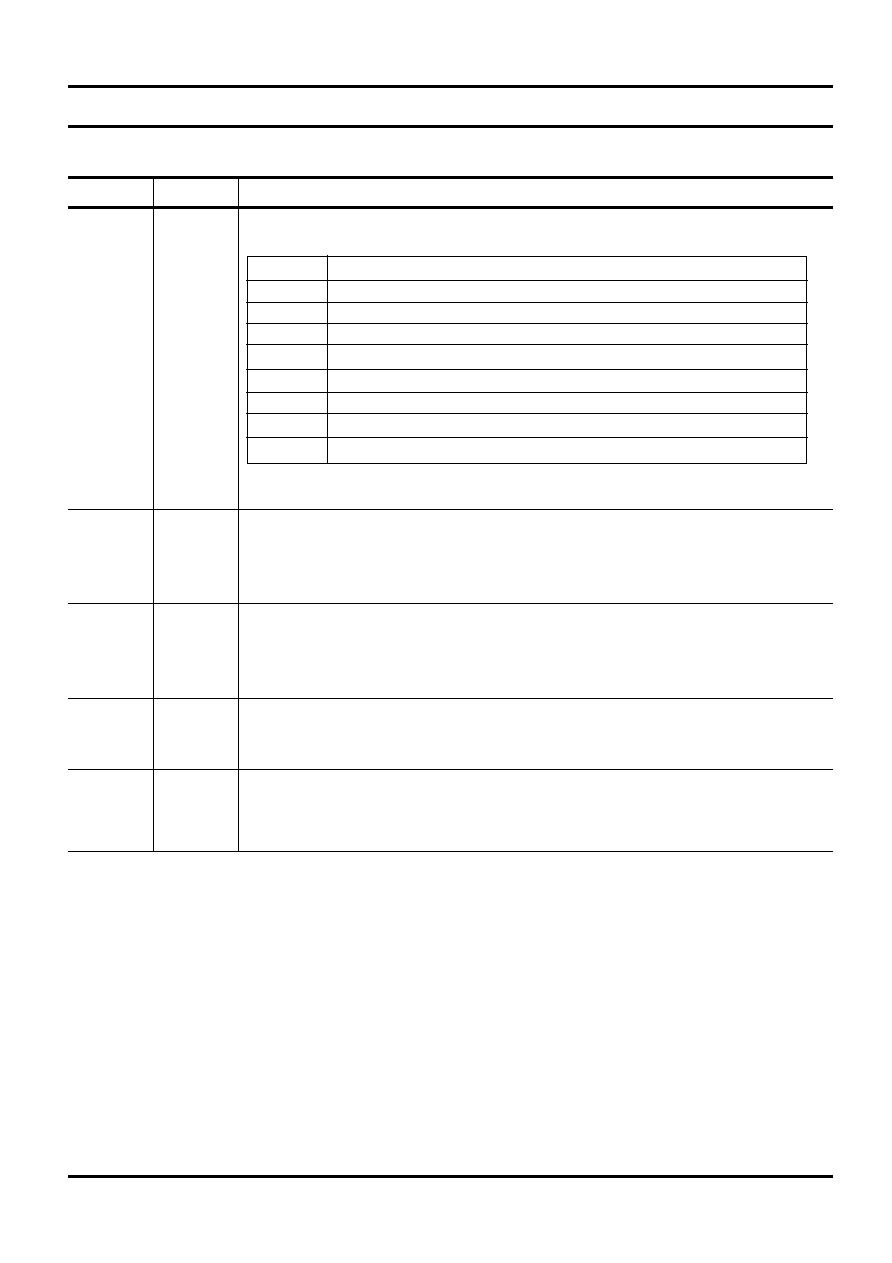
Pin Description
Pin #
Symbol
Function
23
M1
Microphone Inputs
24
M2
Differential inputs for the microphone (electret).
3
RO
Receive Output
This is the output for driving a dynamic earpiece with an impedance of 140 to 300
.
5
A
GND
Analogue Ground
This is the analogue ground for the amplifiers.
28
RI
Receive Input
This is the input for the receive signal.
6
STB
Side Tone Balance Input
This is the input for side tone cancellation.
1
LS
Line Current Sense Input
This is the input for sensing the line current.
27
LI
Line Input
This input is used for power extraction and line current sensing.
25
CS
Current Shunt Control Output
This N-channel open drain output controls the external high power shunt transistor for the
modulation of the line voltage and for shorting the line during make period of pulse dialling.
4
V
DD
Positive Voltage Supply
This is the supply pin for the circuit.
26
V
SS
Negative Power Supply
8
MO
Melody Output
PDM output of the melody generator for tone ringing. Hi-Z when not active.
21
FCI
Frequency Comparator Input
This is a Schmitt trigger input for ring frequency discrimination. Disabled during off-hook.
10
HS/DP
Hook Switch Input and Dial Pulse Output
This is an I/O that is pulled high by the hook switch when off-hook and an open drain pulls
it low during break periods of pulse dialling and flash.
11
OSC
Oscillator Input
Pin for ceramic resonator (3.58 MHz). Recommended: Murata CSA 3.58MG312AM.
9
LLC
Line Loss Compensation
Select pin for line loss compensation (see also figure 4 to 7).
LLC = A
GND
: 20 - 50 mA
LLC = V
DD
: 45 - 75 mA
LLC = V
SS
: none.
22
LED
LED Output Driver
Output for driving an LED that will be flashing when in Programme/Mute state.
Continues...
3
Rev. 7
July 1998
Data Sheet
AS2533...6
Pin Description cont¥d
Pin #
Symbol
Function
12
MODE
Signalling Mode Select Input
Mode pin
Function
Open
Dialling inhibited
Row 1
LD mode, 10 pps, 33/66 ms
Row 2
LD mode, 10 pps, 40/60 ms
Row 3
LD mode, 20 pps, 33/66 ms
Row 4
LD mode, 20 pps, 40/60 ms
Row 5
LD mode, 10 pps, 33/66 ms, Temp. MF with tone on first * key entry
Row 6
MF only, 82/82 ms
Row 7
MF only, 82/160 ms
During temporary MF: 82/160 ms
20
R1
Keyboard Rows
19
R2
(see key arrangement in figure 2)
18
R3
17
R4
16
C1
Keyboard Columns
15
C2
(see key arrangement in figure 2)
14
C3
13
C4
7
CI
Complex Impedance Pin
For complex impedance a capacitor should be connected to this pin.
2
MFL
MF Level Setting
A voltage divider connected from this pin to A
GND
and V
SS
can be used to set the DTMF
level.
Selection Overview
Function
AS2533
AS2534B
AS2534E
AS2535
AS2536
Direct memories (one-key)
4
0
0
12
4
Indirect memories (two-key)
10
0
0
0
10
Repeat dialling
yes
yes
yes
no
yes
LNR key
yes
yes
yes
yes
yes
Pause insertion by LNR key
yes
yes
yes
yes
yes
Pause (PS) key
yes
yes
yes
no
yes
P/M or MT key
P/M
P/M
MT
P/M
P/M
Tone/Pulse (T/P) key
yes
yes
yes
no
yes
Temperary MF by * key
yes
yes
yes
yes
yes
Centrex (A - D) keys
yes
yes
yes
no
yes
Volume (VOL, ≠/+) keys
yes
yes
yes
yes
yes
Volume reset by off-hook
yes
no
no
yes
no
Programming of tone ringer
yes
yes
no
yes
yes
R3 Flash duration
600 ms
600 ms
375 ms
600 ms
600 ms

4
Rev. 7
July 1998
Data Sheet
AS2533...6
Keyboard Connections
Key closure, R
ON
max. = 1 kohm
Key open, R
OFF
min. = 1 Mohm
(Either VOL or +/≠ keys)
P
P
/
/
M
M
1
1
2
2
3
3
4
4
5
5
6
6
7
7
8
8
9
9
0
0
*
*
#
#
R
R
1
1
R
R
2
2
R
R
3
3
L
L
N
N
R
R
V
V
O
O
L
L
+
+
≠
≠
A
A
B
B
C
C
D
D
R
R
P
P
P
P
S
S
T
T
/
/
P
P
C1
C2
C3
C4
R1
R2
R3
R4
Figure 2b (AS2534)
P
P
/
/
M
M
1
1
2
2
3
3
4
4
5
5
6
6
7
7
8
8
9
9
0
0
*
*
#
#
R
R
1
1
R
R
2
2
R
R
3
3
L
L
N
N
R
R
V
V
O
O
L
L
+
+
≠
≠
A
A
B
B
C
C
D
D
R
R
P
P
P
P
S
S
T
T
/
/
P
P
M
M
1
1
M
M
2
2
M
M
3
3
M
M
4
4
C1
C2
C3
C4
R1
R2
R3
R4
M
M
R
R
Figure 2a (AS2533/6)
For AS2534E
P/M is MT key.

5
Rev. 7
July 1998
Data Sheet
AS2533...6
Power On Reset
The on chip power on reset circuit monitors the supply
voltage (V
DD
) during off-hook. When V
DD
rises above
approx. 1.2V, a power on reset occurs which clears the
RAM.
DC Conditions
The normal operating range is from 13 mA to 100 mA.
Operating range with reduced performance is from 5 mA
to 13 mA (parallel operation). In the operating range all
functions are operational.
At line currents below 13 mA the AS253x provides an
additional slope below 4.5V in order to allow parallel
operation (see figure 13).
The dc characteristic (excluding diode bridge) is
determined by the voltage at LI and the resistor R1 at line
currents above 13 mA as follows:
V
LS
=
V
LI
+
I
LINE
R1
The voltage at LI is 4.5V in the normal operating range.
During pulse dialling the speech circuit and other part of
the device not operating is in a power down mode to
save current. The CS pin is pulled to V
SS
in order to turn
the external shunt transistor on to keep a low voltage
drop at the LS pin during make periods.
AC Impedance
The ac impedance of the circuit is set by external
components. The impedance can be real or complex.
The ac impedance is determined as follows:
Z
AC
=
33
∑
Z 1
The dc value of Z1 should be 30
to maintain correct dc
performance.
Return loss and side tone cancellation can be determined
independant of each other.
Speech Circuit
The speech circuit consists of a transmit and a receive
path with dual soft clipping, mute, line loss compensation
and sidetone cancellation.
Transmit
The gain of the transmit path is 37 dB for 600
line
termination from M1/M2 to LS (see test circuit figure 10).
Keyboard Connections Continued
(Either VOL or +/≠ keys)
Figure 2c (AS2535)
P
P
/
/
M
M
1
1
2
2
3
3
4
4
5
5
6
6
7
7
8
8
9
9
0
0
*
*
#
#
R
R
1
1
R
R
2
2
R
R
3
3
L
L
N
N
R
R
V
V
O
O
L
L
+
+
≠
≠
M
M
1
1
M
M
2
2
M
M
3
3
M
M
4
4
M
M
5
5
M
M
6
6
M
M
7
7
M
M
8
8
M
M
9
9
M
M
1
1
0
0
M
M
1
1
1
1
C1
C2
C3
C4
R1
R2
R3
R4
M
M
1
1
2
2