 | –≠–Ľ–Ķ–ļ—ā—Ä–ĺ–Ĺ–Ĺ—č–Ļ –ļ–ĺ–ľ–Ņ–ĺ–Ĺ–Ķ–Ĺ—ā: AS2701AT | –°–ļ–į—á–į—ā—Ć:  PDF PDF  ZIP ZIP |

AS2701A (ISA3+)
AS-Interface Slave IC
Data Sheet
Rev. C, October 2000

AS-Interface Slave IC
AS2701A (ISA3+)
Rev. C, October 2000
Page 2 of 16
K e y F e a t u r e s
∑
Simple two-wire bus (AS-Interface line)
∑
Transmission of both power and signal on the AS-Interface line
∑
Decoupling of power and signal by the IC without additional external devices
∑
Transmitting protocol for using the IC and the AS-Interface master in the trans-
mit/receive modes
∑
Switching of max. 31 AS-Interface slave ICs on one bus possible
∑
Power supply of peripheral devices from the AS-Interface slave IC of up to 35mA@24V
∑
Only few external devices necessary for operation (quartz, 4 capacitors, E
2
PROM)
∑
Storing of the configuration data and the slave address in one E
2
PROM
∑
Quartz oscillator for 5.333 MHz without external capacitances
∑
Standards: AS-Interface≠Spec V2.0 and EN 50295
G e n e r a l D e s c r i p t i o n
The signal transmission between the master and the slaves in the AS-Interface system is
performed by a parallel two-line wire (AS-Interface line) to which the IC is connected only via a
polarity protection diode and a suppressor diode. The line is powered by a direct dc voltage of
up to 33.1 V, on which data pulses with signal amplitudes of (3...8) Vpp are superimposed.
The IC extracts its own power and the power for peripherals from the line and detects the bus
signals.
The AS-Interface slave IC consists of the following blocks:
∑
Receive Block
∑
Transmit Block
∑
Digital Logic Block
∑
Emergency Control Block
∑
Internal and External Power Supply with Signal decoupling
∑
Oscillator
∑
Power on Reset
∑
High Voltage I/O
B l o c k D i a g r a m
LTGP
switch
Emergency and
Temperature
Control Block
Receive Block
Transmit Block
Internal Power
Supply
Power-On
Reset
Oscillator
Signal Decoupling
Ext. Power Supply
E
2
-Interface
Digital
Block
HV-
I/O
LTGN
UOUT
CDC
TEST
U5R
SCL
SDA
DSTBn
P0...P3
D0...D3
PSTBn
OSC2
OSC1
imp_pos, imp_neg
AS-Interface Slave IC
AS2701A (ISA3+)
Rev. C, October 2000
Page 3 of 16
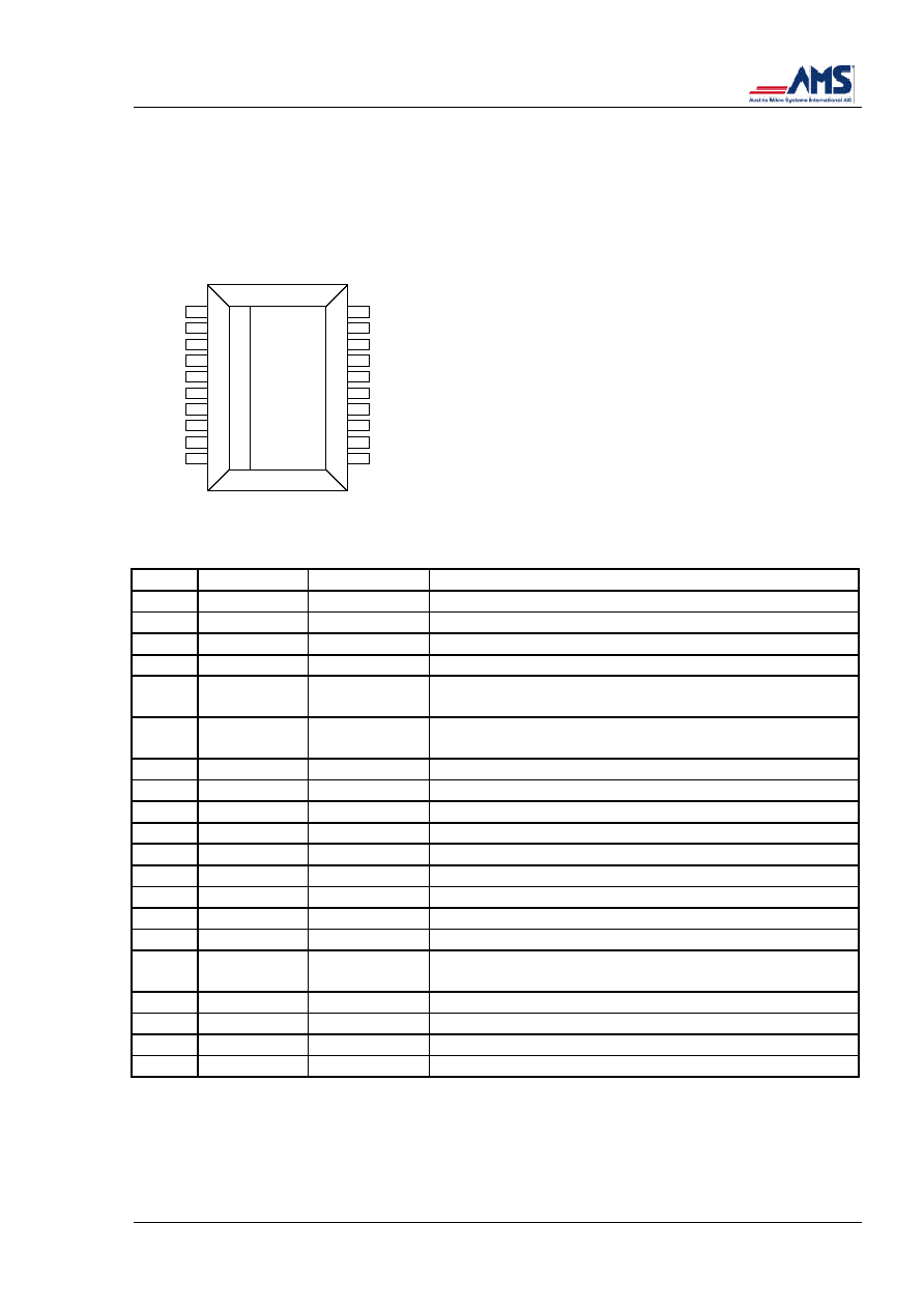
P a c k a g e
SOIC20
P i n D e s c r i p t i o n
1
2
3
4
5
6
7
8
9
10
20
19
18
17
16
15
14
13
12
11
D3
D2
D1
D0
DSTBn
U5R
TEST
SCL
SDA
LTGN
P3
P2
P1
P0
PSTBn
OSC2
UOUT
CDC
LTGP
OSC1
Pin
N a m e
Type
Description
1
D3
I/O
Data input/output 3, configurable
2
D2
I/O
Data input/output 2, configurable
3
D1
I/O
Data input/output 1, configurable
4
D0
I/O
Data input/output 0, configurable
5
DSTBn
I/O
Strobe output for the data port,
input for a reset signal (active low)
6
U5R
Voltage OUT Supply voltage of the E
2
PROM,
Blocking capacitor CU5R
7
TEST
IN
Connection to the capacitor CTEST
8
SCL
OUT
Serial two-wire bus, puls wire
9
SDA
I/O
Serial two-wire bus, address and data wire
10
LTGN
SUPPLY
AS-Interface wire, negative supply
11
LTGP
SUPPLY
AS-Interface wire, positive supply
12
CDC
Voltage OUT Blocking capacitor CCDC
13
UOUT
Voltage OUT Peripherals
14
OSC1
IN
Quartz connection
15
OSC2
OUT
Quartz connection
16
PSTBn
OUT
Strobe output for the parameter port, test mode
(without importance for users)
17
P0
OUT
Parameter output 0
18
P1
OUT
Parameter output 1
19
P2
OUT
Parameter output 2
20
P3
OUT
Parameter output 3

AS-Interface Slave IC
AS2701A (ISA3+)
Rev. C, October 2000
Page 4 of 16
F u n c t i o n a l D e s c r i p t i o n
The IC identifies and decodes the supply voltage overlapping signals of the master telegram. If
the slave address contained within the master telegram coincides with the stored information
in the E
2
PROM of the slave address, the corresponding master command of the addressed
AS-Interface slave IC is executed.
After decoding of the master telegram the addressed AS-Interface slave IC responds with a
corresponding slave answer on the AS-Interface line.
The AS-Interface slave IC extracts its own supply voltage and the supply voltage for the
E
2
PROM from the AS-Interface line. At the same time, the IC provides a direct voltage for the
peripheral UOUT which results from U
LTGP
-U
DROP
for a maximum current of 35 mA.
The receive block detects the signal on the AS-Interface wire LTGP. The reference voltages of
the signal comparators are (52.5 Ī 5) % of the maximum signal value and are controlled by a
peak value detector in the following mode: The comparator level is set to its default value by
Reset or if a non-correct signal is received.
If a line pause is detected, the level reset is released and the IC is able to adapt itself to
different signal levels. If the IC is not synchronized yet, the level adaption is faster (smaller
attack and decay time constants) as in the synchronous case.
The output information of the receive blocks are the signals: "imp_pos" and "imp_neg".
The transmit block drives the output level for the modulated transmit signal edges. The
transmit block consists of the NMOS transistor (transmit transistor), DAC for transmit signal
formation and a Jabber-Inhibit Circuitry. The DAC is addressed by the digital block. If the
transmitter is active more than typ. 300Ķs the Jabber-Inhibit circuit separates the IC from the
AS-Interface line. This condition can only be left by a Power-On-Reset.
In the digital block the received signal is analyzed, the transmit signal is generated and the
data and parameter ports as well as the E
2
PROM interface are driven. The E
2
PROM interface
acts as a serial two-wire interface with the following transmission streams:
After the AS-Interface slave IC has sent the START condition, the device address is
transmitted. This address would allow the selection of a maximum of 8 possible E
2
PROM ICs,
is however fixed to 000 by the AS-Interface slave IC. Therefore in the application pins AO...A2
of the E
2
PROM are connected to Uss.
Device-Address
ACK
1
1
0
0
A2
A1
A0
1
R/W
Data
ACK
P
S
SDA
S
1
1
0
0
A2
A1
A0
0
Device-Address
Byte-Address
ACK
R/W
Byte Read Cycle
ACK
SDA
S
1
1
0
0
A2
A1
A0
0
Device-Address
Byte-Address
ACK
R/W
Byte Write Cycle
Data
ACK
ACK
P

AS-Interface Slave IC
AS2701A (ISA3+)
Rev. C, October 2000
Page 5 of 16
Write Cycle
After the device address, the write cycle R/W-Bit=0, necessary for the identification of the write
cycle, is sent. The E
2
PROM acknowledges the correct receipt with the acknowledge bit ACK.
Then the data byte which should be written into the E
2
PROM reacknowledges with an ACK
signal of the E
2
PROM. The STOP condition ends the cycle.
Read Cycle
The read cycle is similar to the herein described write cycle. In this case the R/W-Bit = 1 which
causes the E
2
PROM to place read data for the received Byte address on the bus after the
acknowledge.
START
Condition
STOP
Condition
SDA
SCL
The START condition is recognized by the E
2
PROM when a H/L edge arises on the dataline
SDA during the high phase of the clock.
The STOP condition is present when a L/H edge arises on the dataline SDA during the high
phase of the clock SCL. The timing of the E
2
PROM interface is derived from the AS-Interface
quartz frequency of 5.333 MHz.
AS-Interface Slave IC
AS2701A (ISA3+)
Rev. C, October 2000
Page 6 of 16
F u n c t i o n a l , e l e c t r i c a l a n d t i m i n g c h a r a c t e r i s t i c s
All voltages are referenced to LTGN = 0V, timing is valid for a clock frequency of 5.333 MHz.
a) Absolute Maximum Ratings
Symbol
Parameter
Min
Max
Unit
Note
VLTGP
Positive Voltage
- 0.3
40
V
1
VLTGPOV
Positive Impulse Voltage
50
V
2
Vin1
Voltage at D0... D3, P0... P3,
DSTBn, PSTBn, CDC, UOUT,
TEST
VLTGN - 0.3
VLTGP + 0.3
V
Vin
40V
Vin2
Voltage at OSC1, OSC2, SDA,
SCL, U5R
VLTGN - 0.3
7
V
Iin
Input Current on every Pin
-25
25
mA
H
Non-Condensated Humidity
3
ESD
Electrostatic Discharge
1000
V
4
STG
Storing Temperature
-55
125
įC
lead
Soldering Temperature
260
įC
5
Ptot
Power Dissipation
1
W
6
Notes:
1 A polarity protection diode is to be used externally
2 Impulse width:
50 Ķs; repetition rate:
0.5 Hz
3 Defined in DIN 40040 cond. F
4 HBM; R = 1.5 k
; C = 100pF
5 260 įC for 10 s (reflow and wave soldering), 360 įC for 3 s (manual soldering)
6 SOIC 20: Rthja = 64.5 įK/W typ.
b) Recommended Operating Conditions
Symbol
Parameter
Min
max
Unit
Note
VLTGP1
Positive Voltage
26.9
33.1
V
1
VLTGP2
Positive Voltage for Sensor
Applications
17.5
33.1
V
2
ILTG
Operating Current @ VLTG = 30 V
6
mA
3
IOL
Max. Operating Current @ D0... D3,
DSTBn
10
mA
IOL
Max. Output Current @ P0... P3,
PSTBn
6
mA
fC
Quartz Frequency
5.333
MHz
4
amb
Operating Temperature
-25
85
įC
Notes:
1 DC Parameter; VLTGP1min = VUOUTmin + VDROPmax;
VLTGPmax = VUOUTmax + VDROPmin
2 DC Parameter; VLTGP2min = VCOMOFFmax + VDROPmax
3 fC = 5.333 MHz, no load on UOUT and U5R, IC in idle mode
4 "AS-Interface-Quartz"

AS-Interface Slave IC
AS2701A (ISA3+)
Rev. C, October 2000
Page 7 of 16
c) Power Supply Pins LTGP and LTGN (LTGN = 0 V-reference)
The AS-Interface Slave IC's input at LTGP behaves as if a resistor RP and a (non-linear)
parallel capacitor CP connect LTGP to LTGN.
LTGP input impedance over frequency is as follows:
RP
CP
F
10 kOhm
35 pF
50 kHz
10 kOhm
45 pF
100 kHz
10 kOhm
48 pF
125 kHz
10 kOhm
51 pF
160 kHz
10 kOhm
54 pF
200 kHz
10 kOhm
60 pF
300 kHz
d) Data and Parameter Ports (D0...D3, DSTBn; P0...P3, PSTBn)
These pins are equipped with both an input and output channel as well as a current source
based pull-up structure; the I/O-circuit at these pins and their DC-characteristics @ output
channel 'Off' are described below.
The AS-Interface slave system concept requires D0...D3 and DSTBn to be bidirectional pins
and P0...P3 and PSTBn to be outputs.
The input channel on pins P0...P3 and PSTBn is only implemented to simplify the AS-Interface
Slave IC's device test, and is not intended to be used in AS-Interface Slave system applica-
tions.
11 ĶA typ
LTGN
D0..D3
DSTBn
P0..P3
PSTBn
U5R
0
-5
-10
-15
-20
4
0
10
20
30
40
VI[V]
II[ĶA]

AS-Interface Slave IC
AS2701A (ISA3+)
Rev. C, October 2000
Page 8 of 16
Symbol
Parameter
min
max
Unit
Note
VIL
Input Voltage "Low"
0
1.5
V
VIH
Input Voltage "High"
3.5
VUOUT V
VHYST
Input Hysteresis
0.25
0.5
V
1
VOL11
Output Voltage
0
1
V
IOL11 = 10mA
D0... D3, DSTBn
VOL12
Output Voltage
0
1
V
IOL12 = 6mA
P0... P3, PSTBn
VOL2
Output Voltage
0
0.4
IOL2 = 2mA
IIL
Input Current
-20
-5
ĶA
VIL = 1V, Output "off"
IIH
Input Current
-10
10
ĶA
VU5R
VIH
40V
Output "off"
CDL
Loading Capacitance
on DSTBn
10
pF
2
Notes:
1 Switching points approx. 2.5 V, i.e. 2.5 V
Ī
VHYST
2 For larger capacitive loads an external Pull-Up-Resistor to UOUT must be used, so that
the beginning of the DSTB = LOW impulse of VIH
3.5 V to DSTBn is reached in less than
35 Ķs, otherwise a reset is the result.
Timing characteristics
Symbol
Parameter
min
max
Unit
Note
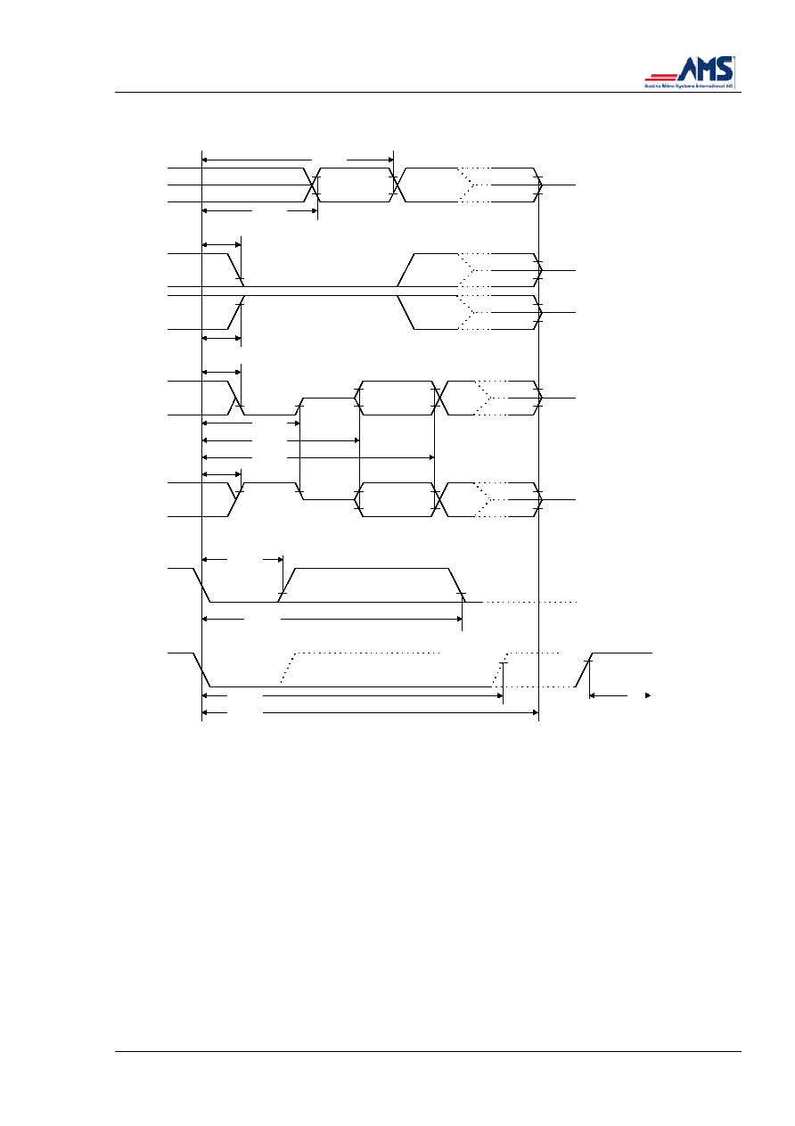
t
DSTBL
DSTBn to D0... D3, Direction OUT,
Output Data LOW
1
Ķs
t
DSTBH
DSTBn to D0... D3, Direction OUT,
Output Data HIGH
1.5
Ķs
t
DATA
DSTBn to D0... D3, High Resistive
6.2
7
Ķs
1
t
DSTB
DSTBn Pulse Width
6
6.8
Ķs
t
DINon
DSTBn to D0... D3, Direction IN, Valid
Input Data
6.5
7.7
Ķs
t
DINoff
DSTBn to D0... D3, End of Direction IN
12.5
t CYCLE
Ķs
t
CYCLE
Next Cycle
150
Ķs
t
ALM1
Extension DSTBn to D0... D3, High
Resistive
44
Ķs
t
ALM2
Extension DSTBn (No Reset)
35
Ķs
Note 1: Data valid until DSTBn L/H-edge
AS-Interface Slave IC
AS2701A (ISA3+)
Rev. C, October 2000
Page 9 of 16
t
DINon
t
DINoff
HI-Z
Direction of Input
Direction of Output
t
DSTBL
t
DSTBH
data in
data out LOW
data out HIGH
HI-Z
HI-Z
t
DSTBL
t
DATA
t
DINon
t
DINoff
data out
data in
data out
data in
HI-Z
HI-Z
t
DSTBH
t
DSTB
t
CYCLE
Bidirectional
(t
RESET1
)
t
ALM2
t
ALM1
HI-Z
HI-Z
D0..D3
D0..D3
D0..D3
D0..D3
D0..D3
DSTBn
DSTB
(ext. LOW)

AS-Interface Slave IC
AS2701A (ISA3+)
Rev. C, October 2000
Page 10 of 16
e) Interface to the ext. E
2
PROM (U5R, SCL, SDA) / functional,
electrical and timing characteristics
Symbol
Parameter
min
max
Unit
Note
VU5R
Output Voltage to E
2
PROM
4.5
5.5
V
IU5R
3 mA
CU5R
Load Capacity to U5R
10
220
nF
Ceramics capacitor
IU5R
Output Current to U5R
3
mA
VOL
Output Voltage "Low"
0
0.2 * VU5R
V
IOL = 10 ĶA
VOH
Output Voltage "High"
0.8 * VU5R
VU5R
V
-IOH = 10 ĶA
VIL
Input Voltage "Low" (only SDA)
-0.3
0.3 * VU5R
V
-IIL = 1.5... 0.2mA
VIH
Input Voltage "High" (only SDA)
0.7 * VU5R
VU5R + 0.3
V
IIH = -1... 1 ĶA
t
DATAinSU
Set-up Time for Data Input
0.25
Ķs
t
DATAinHO
Hold Time for Data Input
0
Ķs
t
AA
Time from SCK Low to SDA
Data Out and ACK Out
3.5
Ķs
t
DATAoutHO
Hold Time for Data Output
0.3
Ķs
t
STARTSU
Set-up Time for Start Condition
4.7
Ķs
t
STARTHO
Hold Time for Start Condition
4
Ķs
t
STOPSU
Set-up Time for Stop Condition
4.7
Ķs
t
BUF
Time which has to be Free for
Bus: Before Next Transmission
4.7
Ķs
t
R
Rise Time
1000
ns
t
F
Fall Time
300
ns
t
LOW
Impulse LOW Time
4700
ns
t
HIGH
Impuls HIGH Time
4000
ns
t
SCL
Clock Frequency for E
2
PROM
100
kHz
fc = 5.333 MHz
SCL
SDA in
SDA out
t
STARTSU
t
LOW
t
DATAinHO
t
DATAoutHO
t
DATAinSU
t
STARTHO
t
F
t
F
t
AA
t
HIGH
t
STOPSU
t
R
t
BUF
t
R
The U5R supply pin provides a typically 5V supply voltage to the external E
2
PROM, and has a
biasing capability only for this purpose.
Programming of the E
2
PROM is possible with the E
2
PROM soldered-in into the AS-Interface
Slave unit's pc-board by accessing the SCL / SDA serial bus with an external programming
hardware.

AS-Interface Slave IC
AS2701A (ISA3+)
Rev. C, October 2000
Page 11 of 16
For successful programming the programmer hardware must have sink/source capability of at
least 5 mA, and the AS-Interface Slave IC's supply voltage LTGP has to be in the range of
26.65 V ...33.35 V.
The only E
2
PROM address locations which can be programmed through the AS-Interface
Slave IC (hence over the AS-Interface Bus and by the AS-Interface Master), are locations 0
and 1, which both have been reserved for the AS-Interface Slave unit's address.
The E
2
PROM has to be programmed in the following way:
E
2
PROM
Address
D7
D6
D5
D4
D3
D2
D1
D0
Initialization Data
0
0
0
0
AS-Interface address
0
1
0
0
0
AS-Interface address
0
2
ID Code
IO Configuration
Custom Specific Data
3
ID Code
IO Configuration
Custom Specific Data
Recommended E
2
PROM types:
Supplier
Type
Organization
Philips
PCA8581P
128 x 8
ST
ST24C01
128 x 8
Catalyst
CAT24LC02(Z)IP
256 x 8
Xicor
X24LC02PI
256 x 8
Catalyst
CAT24LC04(Z)IP
512 x 8
Xicor
X24(L)C04PI
512 x 8
f) Sensor / actuator supply pin UOUT / Functional and electrical
characteristics
Symbol
Parameter
min
max
Unit
Note
VUOUT
Output Voltage at UOUT
VLTGP ≠
VDROP min
VLTGP ≠
VDROPmin
V
IUOUT = 35 mA
VUOUTp
Overswing of the Output
Voltage
1.5
V
CUOUT = 10 ĶF:
Switching 0-35 mA - 0
t
UOUTP
Overswing Impulse Width
2.
ms
VDROP
Voltage Drop from LTGP
to UOUT
5.5
6.7
V
IUOUT
Output Current UOUT
0
35
mA
11.0 V < VUOUT < 27.6 V
CUOUT
Load Capacity UOUT
10
470
ĶF
The interface is intended for the supply voltage to actuators, sensors as well as external
circuits with a power supply of <35mA without overloading the AS-Interface line in the range of
the signal frequency. The AS-Interface slave IC has an internal circuit protector which limits the
current during the charging of the load capacitor and which effects a power down at thermal
overload, e.g. at too high output currents.
In the case of a current break down on the AS-Interface line of less than 1ms, the internally
stored information is retained. The supply voltage of the IC during this time is extracted from
the capacitor Pin UOUT which is disconnected from the AS-Interface line.
AS-Interface Slave IC
AS2701A (ISA3+)
Rev. C, October 2000
Page 12 of 16
Reset Behaviour
The AS-Interface Slave IC can be in reset condition or reset by the following events:
∑
at power-up of VLTGP: as long as VUOUT has not yet reached the treshold voltage
9 V
VCOMOFF
11 V;
∑
at power-down of VLTGP: as soon as U5R drops below the treshold voltage
3.5 V
VPOR
4 V;
∑
by a 'L' input level to DSTBn for more than 44 Ķs;
∑
resulting from a "Reset AS-Interface Slave"- command by the AS-Interface Master
over the AS-Interface BUS.
The different levels of VCOMOFF and VPOR as per a) and b) and the fact that the U5R supply
voltage results from a down-regulation of the VUOUT supply assure a desirable hysteresis in
the order of several volts between the VUOUT power-on-reset and power-down-reset
threshold. Whereas at power-up the AS-Interface Slave IC is released from reset by VUOUT
reaching a level of between 9 V and 11 V, at power-down VUOUT has to come down to a level
in the order of 5 V for U5R to drop into the reset-triggering window between 3.5 V and 4 V.
Some different power-down events are illustrated below:
t
Loff
1
VLTGP
18 V
0 V
POR
(internal signal)
neither receive
nor transmit
2
(no reset)
VUOUT
VCOMOFF
VUOUT
VCOMOFF
VU5R
VPOR
(reset)
3
Notes:
as to (1):
No reset will be triggered, if VLTGP is lower than 18 V for less than 1 ms
as to (2):
If VUOUT < VCOMOFF but still U5R > VPOR, communication over the Data
Port is inhibited, but no reset triggered
as to (3):
If U5R < VPOR (resulting from VUOUT << VCOMOFF), a reset is triggered.
Reset is overcome as soon as VUOUT > VCOMOFF (implying U5R > VPOR)
In reset condition internal registers are cleared and data port D0...D3 is switched into high-
impedant condition. After release from reset the AS-Interface Slave automatically performs a
first read cycle to clear the E
2
PROM from any previously interrupted communication state and
a second one to load the AS-Interface address, IO Configuration and ID Code into its internal
registers.
Symbol
Parameter
min
max
Unit
Note
t reset
Reset Time after the Master
Command "Reset AS-Interface Slave"
or DSTBn = ext. L/H-Edge
2
ms
t reset2
Reset Time after Power On
30
ms
t reset3
Reset Time after Power On with great
Load Capacity
1000
ms
CUOUT = 470 ĶF
t Loff
Voltage Breakdown Time
1
ms
CUOUT > 10 ĶF
VCOMMoff
Voltage for "Communication OFF"
9
11
V
VPOR
Voltage for Internal Reset
3.5
4
V

AS-Interface Slave IC
AS2701A (ISA3+)
Rev. C, October 2000
Page 13 of 16
Application Example 1:
Sensor/actuator circuit supplied by the AS-Interface Slave IC (UOUT) for supply current needs
35 mA.
ASI-Slave-IC
LTGN
SDA
SCL
TEST
U5R
DSTBn
D0
D1
D2
D3
LTGP
CDC
UOUT
OSC1
OSC2
PSTBn
P0
P1
P2
P3
Customer Interface
E
2
PROM
SDA
SCL
TEST
U5R
1
G1
VSS
A2
A1
A0
C1
C3
C5
C2
C4
ASI Line
ASI-N
V2
V1
1
ASI-P
C1 = 22...470 nF / max. AS-Interface BUS DC voltage
C2 = 10...220 nF / max VU5R = 5.5 V
C3 = 10...470 ĶF / max. (VUOUT + VUOUTp) = 29.1 V
C4 = 22...100 nF / max. (VUOUT + VUOUTp + 1.4 V) = 30.5 V
C5 = 10...100 nF (close to the IC) / max. (VUOUT + VUOUTp) = 29.1 V
V1 = 1N4002 or equivalent
V2 = TGL 41-39A or equivalent
G1 = AS-Interface Crystal 5.333 MHz
For V2 a limiter diode with a small capacitance value should be selected, to ensure that the
AS-Interface Bus can be operated with the maximum number of Slave units connected.
In a more general sense care should be taken that the pc board tracks and the external
components between the AS-Interface Bus and LTGP / LTGN contribute to the AS-Interface
Slave unit's input impedance inductively and highly resistively, rather than capacitively.

AS-Interface Slave IC
AS2701A (ISA3+)
Rev. C, October 2000
Page 14 of 16
Application Example 2:
Sensor / actuator circuit supplied from the AS-Interface Bus for supply current needs > 35 mA.
It is recommended to protect the AS-Interface Bus by a fuse in this set-up, if there is a high risk
of excessive current extraction due to component failure (e.g.: MC1747 or other components in
the sensor / actuator circuitry).
ASI-Slave-IC
LTGN
LTGP
CDC
DSTBn
PSTBn
OSC1
OSC2
P0
P1
P2
P3
SDA
SCL
TEST
U5R
UOUT
D0
D1
D2
D3
U1
10
11
12
5
16
14
15
17
18
19
20
9
8
7
6
13
4
3
2
1
E
2
PROM
VCC
VSS
MODE
SCL
SDA
E0
E1
E2
8
4
5
7
6
1
2
3
A
K
C
E
11
10
4
5
7
8
U+
-
+
U-
RF
100n
100n
100n
10Ķ
100n100n
12k
130k
2,2mH 2,2mH
2,2mH 2,2mH
130k
100n
100n
ASI-P
ASI-N
MC1747
ST24C01
AS-Interface Quartz 5.333 MHz
AS2701A works fine with the following crystal types:
Citizen CM 309
Philips SQ 4849
AS-Interface quartz crystals are available from:
Endrich GmbH
Geyer electronic
Contact: Axel Gensler
Contact: JŁrgen Blank
Hauptstr. 56
Camerloherstr. 71
D-72202 Nagold
D-80689 MŁnchen
Tel.: +49-7452-6007-31
Tel.: +49-89-546868-13
Fax: +49-7452-6007-70
Fax: +49-89-546868-90
Email: a.gensler@endrich.com

AS-Interface Slave IC
AS2701A (ISA3+)
Rev. C, October 2000
Page 15 of 16
Kinseki Europe GmbH
Rutronik Elektronische Bauelemente GmbH
Contact: Dirk Holstein
Contact: JŁrgen Tischhauser
Schirmer Str. 76
IndustriestraŖe 2
D-40211 DŁsseldorf
D-75228 Ispringen / Pforzheim
Tel.: +49-211-36815-33
Tel.: +49-7231-801543
Fax: +49-211-36815-10
Fax: +49-7231-801633
Email: dholstein@kinseki.de
Email: juergen_tischhauser@rutronik.com
Application Support
a) For general information and documentation on the AS-Interface concept you may contact
one of the following AS-Interface Associations:
AS-International Association
Contact: Rolf Becker
Zum Taubengarten 52
D-63571 Gelnhausen
Tel.: +49-6051-473212
Fax: +49-6051-473282
Email: as-interface@t-online.de
AS-Interface Switzerland
AS-Interface France
Contact: Rainer Schnaidt
Contact: Gilles Mazet
BittertenstraŖe 15
5 rue Nadar
CH-4702 Oensingen
F-92566 Rueil Malmaison cedex
Tel.: +41-62-388-2567
Tel.: +33-1-41-298294
Fax: +41-62-388-2525
Fax: +33-1-41-298482
Email: rainer.schnaidt@fho.ch
Email: gilles_mazet@mail.schneider.fr
AS-Interface Italy
AS-Interface The Nederlands
Contact: Maurizio Ghizzoni
Contact: Andre Braakman
Via G.B. Barinetti, 1
Boerhaavelaan 40
I-20145 Milano
NL-2700 AD Zoetermeer
Tel.: +39-02-66761
Tel.: +31-79-353-1269
Fax: +39-02-6676-3491
Fax: +31-79-353-1365
Email: maurizio.ghizzoni@siemens.it
Email: ABA@FME.NL
AS-Interface Great Britain
AS-Interface USA
Contact: Geoff Hodgkinson
Contact: Michael Bryant
1 West Street
16101 N. 82
nd
Street, Suite 3B
GB-PO 14 4DH Titchfield, Hampshire
USA-85260 Scottsdale, Arizona
Tel.: +44-1329-511882
Tel.: +1-480-368-9091
Fax: +44-1329-512063
Fax: +1-480-483-7202
Email: asi_uk@gghcomms.demon.co.uk
Email: mbryant@goodnet.com

AS-Interface Slave IC
AS2701A (ISA3+)
Rev. C, October 2000
Page 16 of 16
AS-Interface Belgium
AS-Interface Sweden
Contact: Maurice de Smedt
Contact: Lars Mattsson
Avenue Paul Hymanslaan 47
Karl NordstrŲms všg 31
B-1200 Bruxelles-Brussel
SE-43253 Varberg
Tel.: +32-2-771-3912
Tel.: +46-3406-29270
Fax: +32-2-771-1264
Fax: +46-3406-77190
Email: m.desmedt@udias.be
Email: lars-mattsson@marknadspartnermol.se
b) A demoboard, equipped with AS2701A and supporting discrete components, is available
from:
Bihl & Wiedemann GmbH
Leuze electronic GmbH
Mr. Bihl
Mr. Keller
Kšfertaler StraŖe 164
In der Braike 1
D-68167 Mannheim
D-73277 Owen/Teck
Tel.: +49-621-339-2723
Tel.: +49-7021-573-248
Fax: +49-621-339-2239
Fax: +49-8021-573-200
c) Technical hotline assistance is provided by:
Bihl & Wiedemann GmbH (see above)
Bibliography
ASI: The Actuator-Sensor-Interface for Automation
Edts.: Werner Kriesel, Otto W. Madelung
Carl Hanser Verlag, Munich and Vienna, 1995
ISBN: 3-446-18265-9
Ordering Information
AS2701A
Package: SOIC 20
Delivery: Tubes
AS2701AT
Package: SOIC 20
Delivery: Tape & Reel
Copyright
©
2000, Austria Mikro Systeme International AG, SchloŖ Premstštten, 8141 Unterpremstštten, Austria.
Telefon +43-(0)3136-500-0, Telefax +43-(0)3136-52501, E-Mail info@amsint.com
All rights reserved. No part of this publication may be reproduced, stored in a retrieval system, or transmitted, in any form or by any
means, without the prior permission in writing by the copyright holder. To the best of its knowledge, Austria Mikro Systeme International
asserts that the information contained in this publication is accurate and correct.