 | –≠–ª–µ–∫—Ç—Ä–æ–Ω–Ω—ã–π –∫–æ–º–ø–æ–Ω–µ–Ω—Ç: AS2702 | –°–∫–∞—á–∞—Ç—å:  PDF PDF  ZIP ZIP |

$6 6$3�
$6,QWHUIDFH 6ODYH ,&
'DWD 6KHHW
5HY & -DQXDU\

AS-Interface Slave IC
AS2702 (SAP4.1)
Rev. C, January 2001
Page 2 of 18
.H\ )HDWXUHV
∑
Interface Device to connect Actuators and Sensors to an AS-Interface Bus
∑
Conforms to AS-Interface Spec. V2.11
∑
DC Power Extraction from the AS-Interface Bus
∑
Serial bidir. Data Communication with the Bus
∑
Data Communication Watchdog
∑
4-Bit bidir. Data Port plus Strobe to poll the Sensors and control the Actuators con-
nected
∑
4-Bit Parameter Port plus Strobe to provide Settings to the Sensors and Actuators
∑
24V Power Supply for the Sensors and Actuators
∑
Periphery Fault Input to signal Hardware Failure of the Sensors and Actuators
∑
Integrated 16 x 8 Bit EEPROM to store (5 + 1)-Bit Slave Address and Settings
∑
2 LED Outputs to optically flag Slave Unit Operation Status
∑
Operating Temperature Ta:
- 25 ∞C ... + 85 ∞C
∑
Operating Supply Voltage / Bus DC Voltage:
typ. 30 V
∑
Operating Current (Osc. on, Outputs idle):
6 mA
∑
Supply for Sensors / Actuators:
typ. 24 V,
50 mA
∑
Package:
SOIC 20 for full Functionality;
SOIC 16 for Applications not requiring the Parameter Port
*HQHUDO 'HVFULSWLRQ
AS2702 (SAP4.1) is a new generation AS-interface slave device conforming to AS-interface-
specification V2.11, which supports AS-interface bus systems with up to 62 slave modules.
Each slave module is equipped with an AS2702 device, which interfaces the module to the
unshielded 2-wire AS-interface bus for serial bidirectional data communication and power ex-
traction.
Data communication over the AS-interface bus takes place in master slave fashion, which
foresees that all slave devices AS2702 connected to the bus are sequentially and cyclicly ad-
dressed by a single, central master unit. Data on the AS-interface bus are Manchester en-
coded and can be found as sin2-pulses with a Vpp of between 3V and 8V on top of the bus'
dc voltage of nominally 30V.
AS2702 regulates the nominal dc bus voltage of 30V internally down to 5V to supply it's inter-
nal circuitry including a 16 x 8 bits EEPROM, as well as down to a nominal supply level 24V
with a max. loading of 50 mA for the actuators and sensors connected to it at the field side.
Each slave device AS2702 may interface to up to 4 sensors or 3 actuators. An AS-interface
bus system based on AS2702 may hence link as many as 248 sensors or 186 actuators to a
single master unit.
Slave device AS2702 (SAP4.1) is system compatible with predecessor device AS2701A
(ISA3+): slave modules equipped with AS2702 (SAP4.1) will run in existing AS-interface bus
systems based on AS2701A (ISA3+).
The AS-interface concept is well established as a standardized digital bus system for indus-
trial automation.
AS-Interface Slave IC
AS2702 (SAP4.1)
Rev. C, January 2001
Page 3 of 18
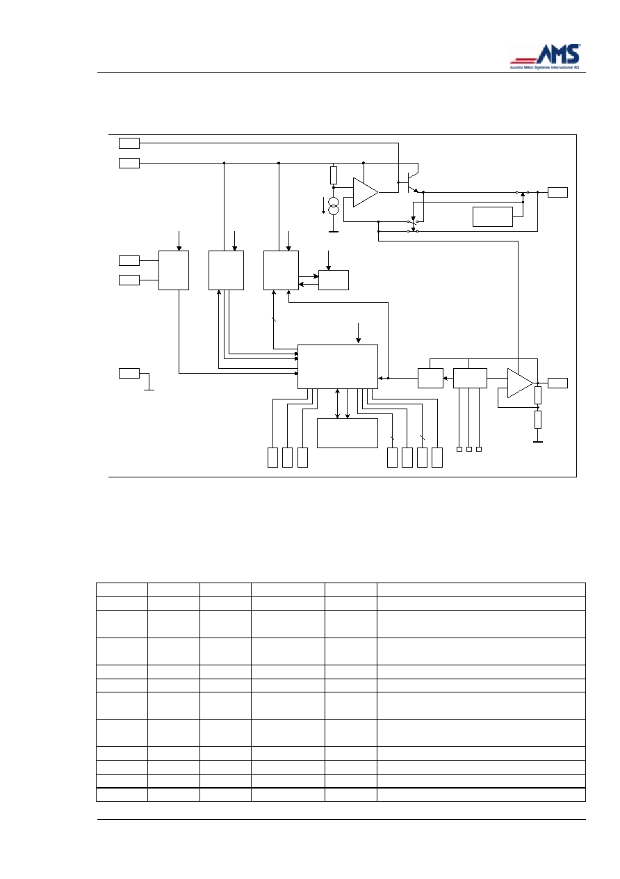
%ORFN 'LDJUDP
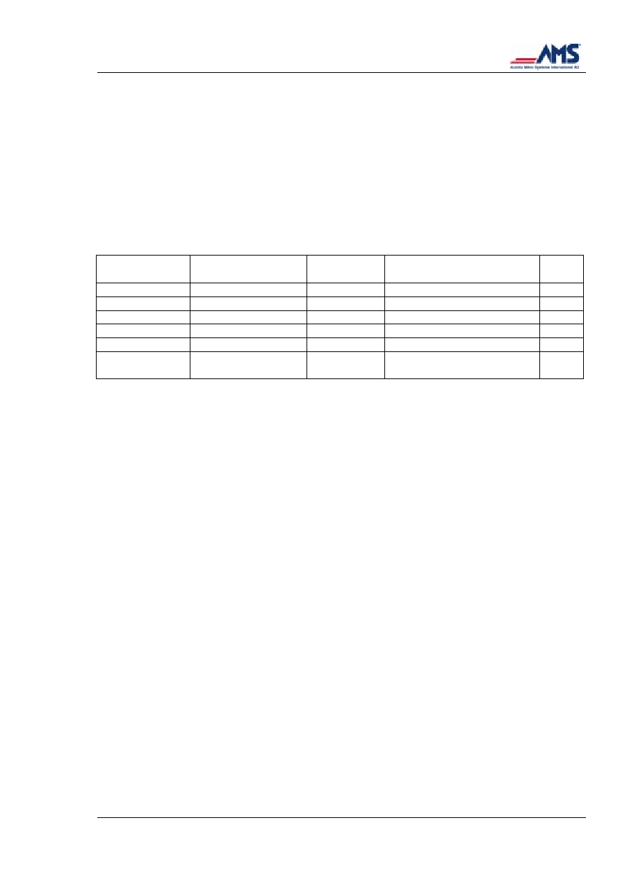
3LQ $VVLJQPHQW DQG 'HVFULSWLRQ
62,& 62,& 1DPH
7\SH
1RWH
'HVFULSWLRQ
Pin Nr.:
Pin Nr.:
1
--
P1
I/O, digital,
pull-up
1, 2
Bidir. parameter port bit 1
2
--
P0
I/O, digital,
pull-up
1, 2
Bidir. parameter port bit 0
3
1
D1
I/O, digital
Bidir. data port bit 1
4
2
D0
I/O, digital
Bidir. data port bit 0
5
3
DSTBn
I/O, digital,
pull-up
1
Data port strobe output; reset-input
6
4
LED1
I/O, digital,
pull-up
1
LED output 1 (IC test input)
7
5
OSC2
O, analog
Output to quarz crystal
8
6
OSC1
I, analog
Input from quartz crystal
9
7
U5R
O, power
Nom. 5V power supply output
10
8
LTGN
I, power
Neg. supply pin, connected
LTGP
LTGN
UOUT
CDC
U5R
OSC2
OSC1
OSCIL-
LATOR
RECEIVE
TRANSMIT
JABBER
INHIBIT
U5R
U5R
U5R
U5R
V
LTGP
-6V
THERMO-
DETECTOR
+
-
+
-
BANDGAP
PORN
TRIMMING
U5R
16 x 8 BIT
SERIAL E
2
PROM
11
IMP_POS
IMP_NEG
RESET
threshold
DS
TB
n
P0
...P3
D
0
...D
3
PST
Bn
SC
L
SD
A
PF
AU
LT
LED
1
4
4
LED
2
LOGIC BLOCK

AS-Interface Slave IC
AS2702 (SAP4.1)
Rev. C, January 2001
Page 4 of 18
to neg. AS-interface bus line;
ground reference.
11
9
LTGP
I, power
Pos. supply pin, connected
to pos. AS-interface bus line
12
10
CDC
I/O, analog
Pin for ext. buffer capacitor
13
11
UOUT
O, power
Nom. 24V power supply output
14
12
PFAULT I, digital, pull-
up
1
Low-active input to flag failure
of the sensors / actuators circuitry con-
nected
15
13
LED2
I/O, digital,
pull-up
1
LED output 2 (IC test input)
16
14
PSTBn
I/O, digital,
pull-up
1
Parameter port strobe output
(IC test input)
17
15
D3
I/O, digital
Bidir. data port bit 3
18
16
D2
I/O, digital
Bidir. data port bit 2
19
--
P3
I/O, digital,
pull-up
1, 2
Bidir. parameter port bit 3
20
--
P2
I/O, digital,
pull-up
1, 2
Bidir. parameter port bit 2
Notes:
1
The pull-up structure is a passive high-side current source with a nom. 10 µA current
2
The passive pull-up current source as per note 1 on these parameter port pins is off,
if the slave device is programmed with I/O-configuration code 7 and a master data
call is present
)XQFWLRQDO HOHFWULFDO DQG WLPLQJ FKDUDFWHULV
WLFV
All voltages are referenced to ground pin LTGN. Timing is valid for a quartz crystal frequency
of 5.333 MHz.
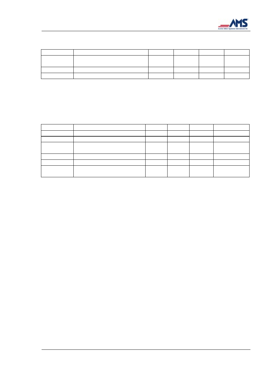
a) Absolute maximum ratings
6\PERO 3DUDPHWHU
0LQ
0D[
8QLW
1RWH
VLTGP
Voltage at the positive supply pin
- 0.3
40
V
1
VCDC
Volage at pin for ext. buffer capacitor
- 0.3
VLTGP +
0.3V
V
VU5R
Voltage at pins U5R, OSC1, OSC2
- 0.3
7
V
IIN
Input current at any pin, except for LTGP,
CDC
- 50
50
mA
2
ESD1
Electrostatic discharge voltage
1500
V
3
ESD2
Electrostatic discharge voltage
200
V
4
STG
Storage temperature
- 55
125
V
LEAD Solder temperature
260
∞C
5
PTOT
Max. power dissipation
1
W
6
RTHJA
Thermal resistance SOIC 16
61.2
74.8
∞K / W
7
RTHJA
Thermal resistance SOIC 20
58.5
71.5
∞K / W
7
AS-Interface Slave IC
AS2702 (SAP4.1)
Rev. C, January 2001
Page 5 of 18
Notes:
1
50 V during t > 50 µs; repetition rate < 0.5 Hz
2
Latch-up immunity test. Pls. observe max. power dissipation allowed.
3
Human body model: R = 1.5 kOhm; C = 100 pF
4
Machine model; applies only for LTGP-LTGN
5
260 ∞C during 10 s (reflow and wave soldering); 360 ∞C during 3 s for manual solder-
ing. Twofold reflow soldering is acceptable.
6
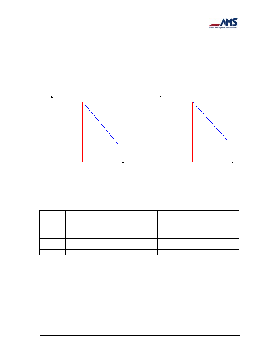
Free convection, see fig. 1
7
No forced cooling. PCB-surface: 21 cm2; still air volume around the device: 10 cm
3
Fig. 1: Max. acceptable power dissipation relative to ambient temperature
b) Recommended Operating Conditions
6\PERO
3DUDPHWHU
PLQ
QRP
PD[
8QLW
1RWH
VLTGP
Positive supply voltage / dc
portion
17.5
34
V
1
ILTG
Supply current consumption
6
mA
2
OA
Ambient temperature
- 25
25
85
∞C
3
FC
Quartz frequency
5.3333
33
MHz
4
Sensitivity against moisture
5
Notes:
1
False-poling protection diode to be inserted between pos. AS-interface bus line and
LTGP-pin. LTGP-pin to be protected furthermore with a voltage clamp between
LTGP and LTGN.
2
Oscillator on; data transmission stage off; no loads connected
3
Power dissipation restrictions as per fig. 1 to be observed
4
ASI Quarz
5
Level 5 acc. to JEDEC-standard JESD22-A112, Table 1
1
0,5
50
100
t/ ∞C
Pv/ W
1
0,5
50
100
t/ ∞C
Pv/ W
62,&
62,&
AS-Interface Slave IC
AS2702 (SAP4.1)
Rev. C, January 2001
Page 6 of 18
F� 6XSSO\ SLQ /7*3
Positive supply pin connected to positive AS-interface bus line and clamped relative to neg.
supply pin / ground LTGN as described under Recommended Operating Conditions.
VLTGP and ILTG specified under Recommended Operating Conditions as well.
6\PERO 3DUDPHWHU
PLQ
PD[
8QLW
1RWH
VSIG
VPP of sin2-data-pulses
on top of dc supply voltage
3
8
V
Z
Input impedance
between 50 kHz and 300 kHz
40
pF
CCDC = 100 nF
1
18
kOhm
1
50
mH
1
Note:
1
Input equivalent circuit is parallel arrangement of C, R and L
G� %XIIHU SLQ &'&
An external buffer capacitor with a recommended value of 100 nF should be connected to this
pin to ensure a sufficiently high input impedance Z at power supply pin LTGP.
Voltage at this pin can be as high as VLTGP.
H� 1RP 9 SRZHU VXSSO\ RXWSXW 8287
The supply output voltage at UOUT is directly derived from VLTGP and regulated to a level
with an offset of about - 6V relative to VLTGP.
UOUT provides bias to the sensors and actuators circuitry connected to the slave device as
well as to the LEDs connected to outputs LED1 and LED2.
UOUT is equipped with a thermal overload protection, which foresees that VUOUT is switched
off as soon as the slave device's substrate temperature TJ passes a threshold value in the
range of (155 -+ 20)∞C.
After TJ has come down and has passed a temperature threshold about (15 -+ 5)∞C lower
than (155 -+ 20)∞C and after a consecutive minimum delay of 1 s has elapsed, VUOUT is
switched on again.
6\PERO
3DUDPHWHU
PLQ
PD[
8QLW
1RWH
VUOUT
Power supply output voltage
VLTGP -
6.3V
VLTGP -
5.3V
V
IUOUT
Load current
50
mA
1
VCOMOFF
UOUT voltage level
9.5
10.5
V
below which data transmission
is inhibited
CUOUT
Buffer capacitor
10
µF
2
Notes:
1
In case IUOUT > 40 mA and presence of sin2-data pulses on LTGP

AS-Interface Slave IC
AS2702 (SAP4.1)
Rev. C, January 2001
Page 7 of 18
with VSIG > 3V, VUOUT may drop as much as 1V below it's level
in unloaded condition
2
Electrolythic and rf filter capacitor in parallel
I� 1RP 9 SRZHU VXSSO\ RXWSXW 85
The voltage at U5R is derived from the voltage present at UOUT, as long as UOUT is not
switched off due to overload. In the latter case U5R is derived from an alternative voltage out
of the UOUT voltage regulator, which is more or less similar to VUOUT in non switched off
condition of UOUT. As a result VU5R is not affected by overload condition at UOUT and will
remain.
6\PERO
3DUDPHWHU
PLQ
PD[
8QLW
VU5R
Power supply output voltage
4.85
5.15
V
IU5R
Load current
1
mA
CU5R
Buffer capacitor
100
nF
J� 2VFLOODWRUSLQV 26& DQG 26&
The only component to be connected to these pins is a quartz crystal with a resonance fre-
quency of 5.333333 MHz (AS-Interface quartz crystal).
6\PERO
3DUDPHWHU
PLQ
PD[
8QLW
CX2
Stray capacitance
10
pF
K� 'DWD SRUW SLQV ' ´ ' DQG GDWD VWUREH SLQ '67%Q
Basically data port D3, ..., D0 is designed for bidirectional data transfer out of and into the
slave device. Each data port pin is equipped with both a low-side open-drain output stage as
well as an input stage to this purpose.
Depending on the so called IO-configuration code, written into and stored in the slave device,
each data port pin is individually set to behave as
∑
output, or
∑
output / input, or
∑
input.
The timing of the data transfer is presented in fig. 2.
Strobe signal DSTBn flags and governs the data transfer as follows:
ha) data port pin is set `output':
output data become valid upon the HL-edge of the strobe and will remain so until the next
HL-edge, hence during the entire strobe cycle;
hb) data port pin is set `output / input':
output data become valid upon the HL-edge of the strobe and will remain so until it's LH-
edge; input data to be valid within a specific time window relative to the HL-edge, after
completion of the strobe's L-phase;
hc) data port pin is set `input':
AS-Interface Slave IC
AS2702 (SAP4.1)
Rev. C, January 2001
Page 8 of 18
input data to be valid within a specific time window relative to the HL-edge of the strobe,
after completion of the strobe's L-phase.
If necessary, output data as per ha) and hb) can be easily latched with the LH-edge of strobe
DSTBn as they will remain valid for about 0.4 µs beyond as a minimum.
Care must be taken however, that signal delay added by external circuitry is lower for the
strobe than for the data.
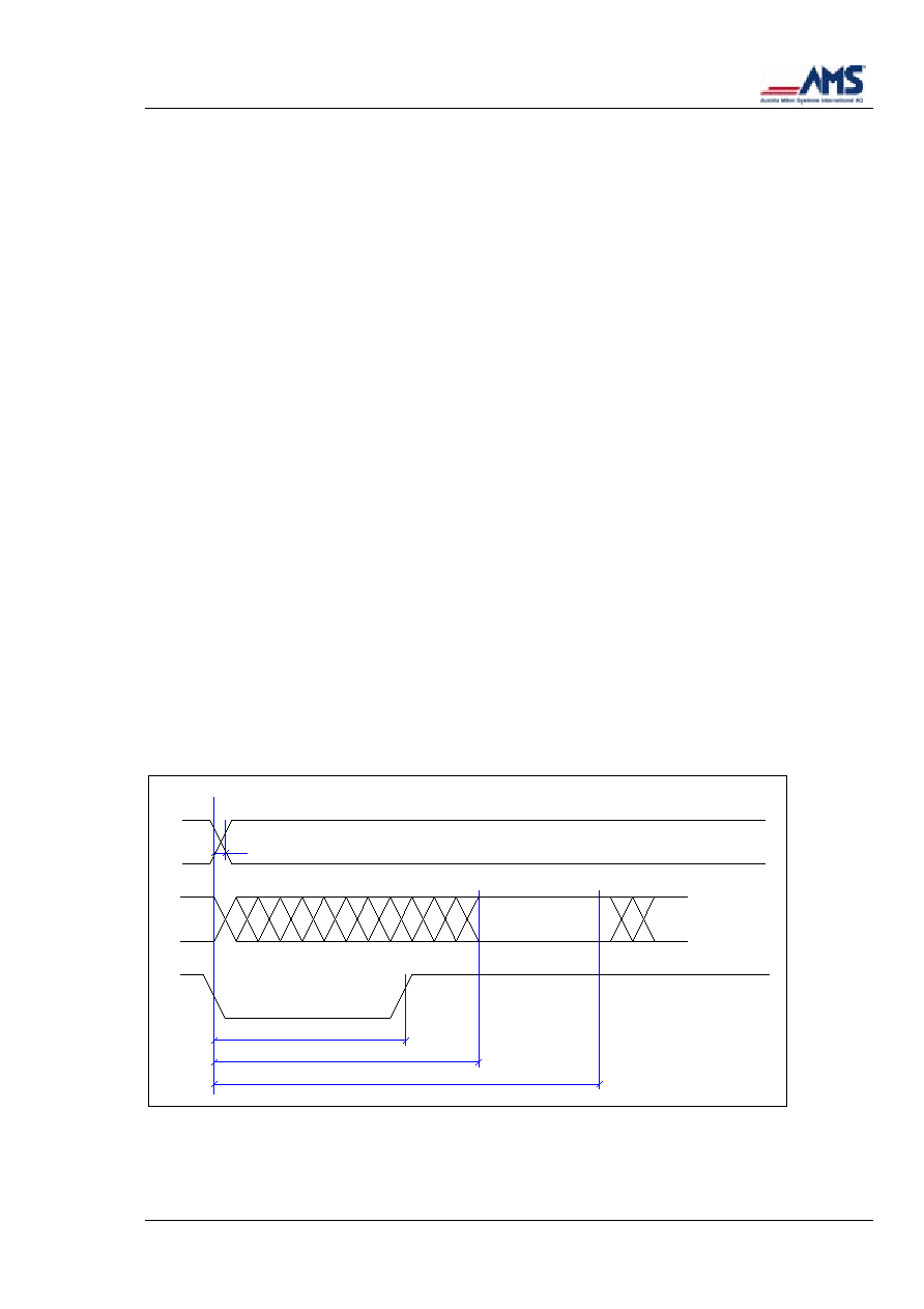
Fig. 2: Timing of data transfer at data port D3, ..., D0 relative to strobe DSTBn
The following table specifies the timing parameters relating to fig. 2:
6\PERO
3DUDPHWHU
PLQ
PD[
8QLW
1RWH
tSTB
Delay DSTBn HL-edge to Dx
output data valid
1.5
µs
tDSTBn
DSTBn strobe width
6
6.8
µs
1
tOUTOFF
Delay DSTBn LH-edge to Dx
output off
0.2
1
µs
2
tINP
Input data valid time window
10.5
12.5
µs
3
Notes:
1
Pulse width depends substantially on value of external pull-up resistor
2
Applies only to data port pins set to 'output / input' operation
3
Timing reference is DSTBn HL-edge.
Applies only to data port pins set to either 'output / input' or 'input' operation
Data in
Data out
Data in
Data out
t
STB
t
DSTBn
+ 0.4 µs
t
DSTBn
+ t
OUTOFF
t
DSTBn
t
INPmin
t
INPmax
Dx
Dx
DSTBn

AS-Interface Slave IC
AS2702 (SAP4.1)
Rev. C, January 2001
Page 9 of 18
The dc-parameters of the data port pins D3, ..., D0 are specified as follows:
6\PERO
3DUDPHWHU
PLQ
PD[
8QLW
1RWH
IOUTLO
Sink current @ output L
10
mA
VOUT =
1V
IOUTHI
Leakage current @ output off
- 1
1
µA
1
VSCHLT
Input threshold voltage
2.5
3.5
V
2
VIN
Acceptable input voltage @
output off
- 0.3
40
V
Notes:
1
Output stage is low-side open-drain; ext. pull-up resistor required as no pull-up
structure on chip
2
No hysteresis implemented
To govern the data transfer at data port D3, ...,D0 strobe pin DSTBn is equipped with a low-
side open-drain output switch plus a passive high-side current source with a nom. 10 µA pull-
up current capability.
However a second function is assigned to the DSTBn pin which requires it to be input as well:
if a low-pulse is imposed on DSTBn by external means with a pulse width of at least 50 to 100
ms, the slave device will be put in RESET condition, as described in section "Reset".
The dc-and timing parameters of strobe pin DSTBn are specified as follows:
6\PERO
3DUDPHWHU
PLQ
PD[
8QLW
1RWH
IOUTLO
Sink current @ output L
10
mA
VOUT = 1V
IOUTHI
Leakge current @ output off
- 10
10
µA
VOUT = 5V
IINLO
Input current @ VIN = 1V
- 5
- 20
µA
1
VSCHLT
Input threshold voltage
1.5
3.5
V
2
VIN
Acceptable input voltage @
output off
- 0.3
40
V
tNORESET
DSTBn L-phase width, not
triggering RESET
50
ms
tRESET
DSTBn L-phase width, trig-
gering RESET
100
ms
CPINEXT
Stray capacitance
20
pF
Notes:
1
DSTBn is equipped with an on-chip pull-up current source, which ensures
a sufficiently fast LH-edge upon output switch-off in open-pin condition,
to prevent erroneous RESET triggering.
If DSTBn has an external load connected to it,
an additional external pull-up resistor may be needed
to prevent erroneous RESET triggering upon output switch-off
2
No hysteresis implemented
AS-Interface Slave IC
AS2702 (SAP4.1)
Rev. C, January 2001
Page 10 of 18
L� 3DUDPHWHU SRUW SLQV 3 ´ 3 DQG SDUDPHWHU VWUREH SLQ 367%Q
(Note that parameter port pins P3, ..., P0 are only available on AS2702 package option SOIC
20, not on the SOIC 16 option.)
The transfer of data at P3, ..., P0 and the supporting strobe action at pin PSTBn takes place
similarly as at D3, ..., D0 resp. DSTBn.
Each parameter port pin P3, ..., P0 is equipped with both a low-side open-drain output switch
plus a passive, but switchable high-side current source with a nom. 10 µA pull-up current ca-
pability, and with an input stage.
Though equipped for bidirectional data transfer as D3, ..., D0, the parameter port is less flexi-
ble than the data port.
Basically the parameter port is set to behave portwise as
∑
output, or
∑
input
depending on the IO-configuration code, written into and stored in the slave device.
The timing of the data transfer is presented in fig. 3.
Strobe signal PSTBn flags and governs the data transfer as follows:
ia) parameter port is set `output':
output data become valid upon the HL-edge of the strobe and will remain so until the
next HL-edge, hence during the entire strobe cycle;
ib) parameter port is set `input':
input data to be valid within a specific time window relative to the HL-edge of the
strobe, after completion of the strobe's L-phase.
Output data as per ia) could be easily latched with the LH-edge of strobe PSTBn, if at all nec-
essary.
Fig. 3: Timing of data transfer at parameter port P3, ..., P0 relative to strobe PSTBn
Parameter out Parameter out
Data in
t
STB
t
PSTBn
t
INPmin
t
INPmax
Px
Px
PSTBn
AS-Interface Slave IC
AS2702 (SAP4.1)
Rev. C, January 2001
Page 11 of 18
The following table specifies the timing parameters relating to fig. 3:
6\PERO
3DUDPHWHU
PLQ
PD[
8QLW
1RWH
tSTB
Delay PSTBn HL-edge to Px
output data valid
1.5
µs
tPSTBn
PSTBn strobe width
6
6.8
µs
1
tINP
Input data valid time window
10.5
12.5
µs
2
Notes:
1
Pulse width depends substantially on value of external pull-up resistor
2
Timing reference is PSTBn HL-edge.
Applies only to parameter port set to 'input' operation
The dc-parameters of the parameter port pins P3, ..., P0 are specified as follows:
6\PERO
3DUDPHWHU
PLQ
PD[
8QLW
1RWH
IOUTLO
Sink current @ output L
10
mA
VOUT = 1V
IOUTHI
Leakage current @ output off
- 10
10
µA
VOUT = 5V
IOUTHI7
Leakage current @ output off;
pull-up current source off
- 1
1
µA
VOUT = 5V;
IO-conf. = 7
IINLO
Input current @ VIN = 1V
- 5
- 20
µA
1
VSCHLT
Input threshold voltage
2.5
3.5
V
2
VIN
Acceptable input voltage @
output off
- 0.3
40
V
Notes:
1
The passive high-side current-source provides an about constant input current @
0V <= VIN <= 4V
2
No hysteresis implemented
Though equipped for bidirectional data transfer as D3, ..., D0, the parameter port is never-
theless less flexible than the data port.
Note the following differences:
ik) The parameter port is set portwise, the data port bitwise by the IO-configuration code;
il) The parameter port can only be set to either `output' or `input'. A bidirectional behaviour
within a strobe cycle is not possible;
im) The parameter port is set to `output' as a rule; the only exception occurs in case of IO-
configuration 7 and a master data request, which set it to `input'.
To govern the data transfer at the parameter port P3, ..., P0 strobe pin PSTBn is equipped
with a low-side open-drain output switch plus a passive high-side current source with a nom.
10 µA pull-up current capability. Typically the PSTBn-strobe width is about 6 µs, see fig. 3.
( However to simplify and shorten the component test time of the slave device, the PSTBn pin
is also used as an input. Input low pulses of more than 50 µs each will step and cycle the de-
vice through 3 different testmodes beyond the regular operation as described in this da-
tasheet.)
AS-Interface Slave IC
AS2702 (SAP4.1)
Rev. C, January 2001
Page 12 of 18
The dc- and timing parameters of strobe pin PSTBn are specified as follows:
6\PERO
3DUDPHWHU
PLQ
PD[
8QLW
1RWH
IOUTLO
Sink current @ output L
10
mA
VOUT = 1V
IOUTHI
Leakage current @ output off
- 10
10
µA
VOUT = 5V
IINLO
Input current @ VIN = 1V
- 5
- 20
µA
1
VSCHLT
Input threshold voltage
1.5
3.5
V
2
VIN
Acceptable input voltage @ out-
put off
- 0.3
40
V
tNOTM
PSTBn L-phase width, not trig-
gering testmode
35
µs
tTM
PSTBn L-phase width, triggering
testmode
50
µs
CPINEXT
Stray capacitance
20
pF
Notes:
1
PSTBn is equipped with an on-chip pull-up current source, which ensures
a sufficiently fast LH-edge upon output switch-off in open-pin condition, to prevent
erroneous testmode triggering.
If PSTBn has an external load connected to it, an additional external pull-up resistor
may be needed to prevent erroneous testmode triggering upon output switch-off
2
No hysteresis implemented
2SHUDWLRQ VWDWXV SLQV /(' DQG /('
Pins LED1 and LED2 are both equipped with a low-side open-drain output switch plus a pas-
sive high-side current source with a nom. 10 µA pull-up current capability. They will each have
an LED load connected to UOUT, which will flag the operation status of the slave device, ac-
cording to the following table:
2XWSXW /(' 2XWSXW /(' )ODJJLQJ 3ULRULW\
6ODYH 'HYLFH
2SHUDWLRQ 6WDWXV
5HDVRQ
JUHHQ /('
FRQQHFWHG�
UHG /(' FRQ
QHFWHG�
KLJKHVW ´
ORZHVW�
off
off
Supply voltage off
No supply voltage
on
off
Regular operation
off
on
4
No Data
Communication
Regular, non-zero
slave address coded;
data comm. watchdog
triggered
blinks
on
3
No regular slave
address coded
Slave address = de-
fault zero
blinks
blinks
(alternating with
LED1)
2
Hardware failure in
sensor / acuator
circuitry
Input PFAULT = L
off
blinks
1
External RESET or
Overload at UOUT
pin
DSTBn = L to RESET,
or UOUT switched-off
due to overload
(LED1 and LED2 both also feature an input stage, to simplify component test and shorten test
time of the slave device.)
The dc- and timing parameters of pins LED1 and LED2 are specified as follows:
AS-Interface Slave IC
AS2702 (SAP4.1)
Rev. C, January 2001
Page 13 of 18
6\PERO
3DUDPHWHU
PLQ
PD[
8QLW
1RWH
ILED
Sink current @ output L
10
mA
VOUT = 1V
IOUTHI
Leackage current @ output off
- 10
10
µA
VOUT = 5V
VIN
Acceptable input voltage @ out-
put off
- 0.3
40
V
fBLINK
Blinking frequency
2
3
Hz
'DWD &RPPXQLFDWLRQ :DWFKGRJ
AS2702 is equipped with a watchdog timer to supervise data communication by monitoring
the strobe signals at pins DSTBn and PSTBn.
If a parameter or data strobe is not followed by a consecutive strobe within a time period of
50 ... 100 ms, the watchdog is triggered and initiates a `soft' reset, see section `Reset'
5(6(7
There are 2 categories of reset-events, leading to 2 slightly different reset-conditions of the
slave device:
1) a `hard' reset taking place at power-up and power-down of supply-voltages U5R and
UOUT.
At power-up the slave device leaves reset-condition as soon as U5R has passed 3.75V
and UOUT has passed VCOMOFF = nom. 10V.
At power-down the slave device is forced into reset-condition as soon as U5R drops below
3.75V.
(Tolerance of the threshold voltages referred to is -/+ 5%.)
2) a `soft' reset, resulting from one of the following events:
2.1) Data strobe pin DSTBn is kept L for more than 100 ms;
2.2) Master command `RESET SLAVE' is received;
2.3) Master command `RESET BROADCAST' is received;
2.4) The communication watchdog is triggered.
A `hard' reset event conditions the slave device as follows:
∑
Internal states (counters, flags, ...) are reset
∑
The slave device's receiver is desynchronized from the AS-interface bus
∑
The low-side open-drain output stages at ports D3, ..., D0 and ports P3, ..., P0 are
switched off
∑
Any test-mode will be cancelled.
A `soft' reset has the following consequences:
∑
A regular, nominal 6µs L-phase strobe is generated on both the DSTBn and PSTBn pin
∑
The low-side open-drain output stages at ports D3, ..., D0 and ports P3, ..., P0 are
switched off
∑
Internal states (counters, flags, ...) are reset, however the following states and operations
are not affected:
∑
the timer function which controls blinking of LED1 and LED2
∑
the data communication watchdog
∑
any testmode
∑
any EEPROM write operation.
Remark:
AS-Interface Slave IC
AS2702 (SAP4.1)
Rev. C, January 2001
Page 14 of 18
If UOUT drops below VCOMOFF = nom. 10V data communication with the AS-interface bus is
aborted by the receiver or transmitter of the slave device. As long as U5R does not drop be-
low 3.75V in this situation, no `hard' reset takes place; however the data communication
watchdog will be triggered (unless disabled) and a `soft' reset will result.
((3520
AS2702 has a 16 x 8 Bits serial interface EEPROM on board to store the slave unit's address
and set-up data in a non-volatile fashion.
The EEPROM stores the following data:
((3520
$GGUHVV
'DWD
5HOHYDQW 1U
RI ELWV
3URJUDPPHG E\
1RWH
0, 1
Slave Address
5 + 1
Master (Initialization)
1
2
Settings (EID1)
4
Master (Initialization)
3
Settings (IO-Conf.)
5
Slave unit manufacturer
4
Settings (ID)
5
Slave unit manufacturer
5
Settings (EID2)
5
Slave unit manufacturer
6
Settings (Control-
Code)
5
Slave unit manufacturer
Note
1
6 Bits (A4, ..., A0 + Sel-bit) in extended address mode: 62 slaves addressable;
5 Bits (A4, ..., A0) in non-extended address mode: 31 slaves addressable
Obviously the capacity of the EEPROM is only partially used.
Reading and writing of the EEPROM is performed bytewise and trough temporary, volatile
registers.
Writing of data from the volatile register into the EEPROM takes about 10 ms per byte,
whereas reading takes less than 1 ms per byte.
Upon RESET the EEPROM info is read into temporary registers, including the slave's address
which has been written redundantly into EEPROM locations 0 and 1 before.
The temporary registers receiving the address are compared for similarity; in case of non-
similarity ≠ which e.g. may have been caused by a supply voltage dip during address writing ≠
the slave will flag non-regular operation status / slave address zero.

AS-Interface Slave IC
AS2702 (SAP4.1)
Rev. C, January 2001
Page 15 of 18
$6 ,QWHUIDFH %XV &RPPXQLFDWLRQ
All slaves connected to an AS-interface bus are sequentially and cyclicly called by the master
in a string of individual transactions between the master and each slave unit.
A transaction consists of a 14 bits master request, typically containing the slave's address as
well as data or parameter info, and an immediate acknowledging slave response of 7 bits.
The 14 bits master request - apart from Start Bit ST = 0 and End Bit EB = 1 ≠ has the follow-
ing contents:
∑
1 Control Bit CB: CB = 0 stands for data transfer (typ. data or parameters)
CB = 1 identifies command-type requests
∑
5 Address Bits:
A4, ..., A0
∑
5 Information Bits:
I4, ..., I0 (typ. data or parameters)
∑
1 Parity Bit PB.
AS2702 allows for up to 62 slaves on the same AS-interface bus; this requires a slave ad-
dress extended to 6 bits, hence an extra bit beyond A4, ..., A0.
Information bit I3 is used as the 6
th
address bit in this so-called extended address mode. It is
called Sel-bit, as it is perceived as to select between A-slave (Sel = 0) and B-slave (Sel = 1) at
address location A4, ..., A0.
In non-extended address mode AS2702 is addressed with A4, ..., A0 only - for a max. total of
31 slaves per AS-interface bus system, and is system compatible with existing slave device
AS2701A.
The 7 bits slave response ≠ apart from Start Bit ST = 0 and End Bit EB = 1 ≠ has the following
contents:
∑
4 Information Bits:
I4, ..., I0 (typ. data or parameters)
∑
1 Parity Bit PB.
Detailed descriptions of all types of master requests and corresponding slave responses can
be found in AS-Interface Specification V2.11, obtainable from the AS-International Association
(D) or its local representative, see section "Application Support".

AS-Interface Slave IC
AS2702 (SAP4.1)
Rev. C, January 2001
Page 16 of 18
$SSOLFDWLRQ ([DPSOH
Sensor/actuator circuit supplied by the ASI Slave IC (UOUT) for supply current needs
50 mA.
C1 = 100 nF / 35 V
C2 = 100 nF / 6 V
C3 = 10...470 µF / 30 V
C4 = 22...100 nF / 30 V
V1 = 1N4002 or equivalent
V2 = TGL 41-39A or equivalent
G1 = AS-Interface Crystal 5.333 MHz
$6 ,QWHUIDFH 4XDUW] 0+]
AS2702 works fine with the following crystal types:
Citizen CM 309
Philips SQ 4849
AS-Interface quartz crystals are available from:
Endrich GmbH
Geyer electronic
Contact: Axel Gensler
Contact: J¸rgen Blank
Hauptstr. 56
Camerloherstr. 71
D-72202 Nagold
D-80689 M¸nchen
Tel.: +49-7452-6007-31
Tel.: +49-89-546868-13
Fax: +49-7452-6007-70
Fax: +49-89-546868-90
Email: a.gensler@endrich.com
ASI Line
ASI-P
C2
G1
C1
C3
C4
V2
V1
L
T
G
N
U
5
R
O
S
C
1
O
S
C
2
L
E
D
1
D
S
T
B
n
D
0
D
1
P
0
P
1
L
T
G
P
C
D
C
U
O
U
T
P
F
A
U
L
T
L
E
D
2
P
S
T
B
n
D
3
D
2
P
3
P
2
$6
S
e
n
s
or
/
A
c
t
u
at
o
r
Ci
r
c
ui
t

AS-Interface Slave IC
AS2702 (SAP4.1)
Rev. C, January 2001
Page 17 of 18
Kinseki Europe GmbH
Rutronik Elektronische Bauelemente GmbH
Contact: Dirk Holstein
Contact: J¸rgen Tischhauser
Schirmer Str. 76
Industriestrasse 2
D-40211 D¸sseldorf
D-75228 Ispringen / Pforzheim
Tel.: +49-211-36815-33
Tel.: +49-7231-801-543
Fax: +49-211-36815-10
Fax: +49-7231-801-633
Email: dholstein@kinseki.de
Email: juergen_tischhauser@rutronik.com
$SSOLFDWLRQ 6XSSRUW
For general information and documentation on the AS-Interface concept you may contact one
of the following AS-Interface Associations:
AS-International Association
Contact: Rolf Becker
Zum Taubengarten 52
D-63571 Gelnhausen
Tel.: +49-6051-473212
Fax: +49-6051-473282
Email: as-interface@t-online.de
AS-Interface Switzerland
AS-Interface France
Contact: Rainer Schnaidt
Contact: Gilles Mazet
Bittertenstraþe 15
5 rue Nadar
CH-4702 Oensingen
F-92566 Rueil Malmaison cedex
Tel.: +41-62-388-2567
Tel.: +33-1-41-298294
Fax: +41-62-388-2525
Fax: +33-1-41-298482
Email: rainer.schnaidt@fho.ch
Email: gilles_mazet@mail.schneider.fr
AS-Interface Italy
AS-Interface The Nederlands
Contact: Maurizio Ghizzoni
Contact: Andre Braakman
Via G.B. Barinetti, 1
Boerhaavelaan 40
I-20145 Milano
NL-2700 AD Zoetermeer
Tel.: +39-02-66761
Tel.: +31-79-353-1269
Fax: +39-02-6676-3491
Fax: +31-79-353-1365
Email: maurizio.ghizzoni@siemens.it
Email: ABA@FME.NL
AS-Interface Great Britain
AS-Interface USA
Contact: Geoff Hodgkinson
Contact: Michael Bryant
1 West Street
16101 N. 82
nd
Street, Suite 3B
GB-PO 14 4DH Titchfield, Hampshire
USA-85260 Scottsdale, Arizona
Tel.: +44-1329-511882
Tel.: +1-480-368-9091
Fax: +44-1329-512063
Fax: +1-480-483-7202
Email: asi_uk@gghcomms.demon.co.uk
Email: mbryant@goodnet.com
AS-Interface Belgium
AS-Interface Sweden
Contact: Maurice de Smedt
Contact: Lars Mattsson
Avenue Paul Hymanslaan 47
Karl Nordstrˆms v‰g 31
B-1200 Bruxelles-Brussel
SE-43253 Varberg
Tel.: +32-2-771-3912
Tel.: +46-3406-29270
Fax: +32-2-771-1264
Fax: +46-3406-77190
Email: m.desmedt@udias.be
Email: lars-mattsson@marknadspartnermol.se

AS-Interface Slave IC
AS2702 (SAP4.1)
Rev. C, January 2001
Page 18 of 18
%LEOLRJUDSK\
ASI: The Actuator-Sensor-Interface for Automation
Edts.: Werner Kriesel, Otto W. Madelung
Carl Hanser Verlag, Munich and Vienna, 1995
ISBN: 3-446-18265-9
2UGHULQJ ,QIRUPDWLRQ
AS2702-20T Package: SOIC 20; delivery: tape & reel
AS2702-16T Package: SOIC 16 W; delivery: tape & reel; no parameter port available
AS2702-20
Package: SOIC 20; delivery: tubes
AS2702-16
Package: SOIC 16 W; delivery: tubes; no parameter port available
Copyright
©
2000, Austria Mikro Systeme International AG, Schloþ Premst‰tten, 8141 Unterpremst‰tten, Austria.
Tel. +43-(0)3136-500-0, Fax +43-(0)3136-52501, E-Mail info@amsint.com
All rights reserved. No part of this publication may be reproduced, stored in a retrieval system, or transmitted, in any form or by
any means, without the prior permission in writing by the copyright holder. To the best of its knowledge, Austria Mikro Systeme
International asserts that the information contained in this publication is accurate and correct.