Preliminary Data Sheet
AS3801
Rev. C
1/7
Nov. 98
CDMA/FM TRANSMIT AGC
AMPLIFIER AS3801
Key Features
r
Supports dual mode operation.
r
-45dB to +40db gain control guaranteed.
r
High OIP3 of 15dBm @ max. gain @ -51dBm
input power.
r
Single 3.6V supply.
r
Temperature and supply stabilized.
r
Power down feature.
r
100MHz to 300MHz operation.
r
Silicon BiCMOS process.
r
Miniature surface mount 16 pin, 150 mil SSOP
package.
Compatibility
The AS3801 is designed to be functionally or/and
pin compatible to the following products:
r
RF9909
(RF Micro Devices), pin compat.
r
Q5505
(Qualcomm),
pin compat.
r
CXA3002N (Sony)
General Description
The AS3801 is a gain controlled amplifier designed
for the transmit section of dual mode CDMA/FDM,
TDMA/FDM or FM/FDM cellular phones.
Key specifications like gain range, noise figure, IP3,
temperature range and other specifications are
designed to be in line with the IS-95 standard for
CDMA cellular communications.
The circuit is designed for narrow band IF
applications but can also be used in wideband
applications.
Applications
r
Digital cellular systems with transmission
methods: CDMA/FDM, TDMA/FDM, FM/FDM
and TDMA/TDD.
r
Examples: IS-95 CDMA, IS-54 DAMPS, AMPS,
PWT.
r
Cordless phones analog / digital.
r
General purpose linear IF amp's.
r
WLL / WLAN.
SSOP-16
CDMA+
CDMA-
GND
GND
GND
GND
GND
PWD
OUT-
OUT+
GND
GND
VCC
VCC
VCC
VCTRL
1
2
3
4
5
6
7
8
16
15
14
13
12
11
10
9
AS3801
This document contains information on products under development. Austria Mikro Systeme Intl. AG reserves
the right to change or discontinue this product without notice
.
Austria Mikro Systeme International AG
Preliminary Data Sheet
AS3801
Rev. C
2/7
Nov. 98
Absolut Maximum Ratings (non operating)
Symbol
Parameter
min
max
Unit
Note
VDD
Positive Supply Voltage
-0.5
7
V
GND
Analog Ground
0
0
V
Vin
Voltage at every Input Pin
Gnd-0.5
VDD+0.5
V
Iin
Input Current
(into any pin except supply pins and
except low leakage pin)
-40
40
mA
Iin_15
Input Current into Low Leakage Pin
-25
25
mA
H
Humidity Noncondensing
1)
ESD
Electrostatic Discharge
1000
V
2)
Tstg
Storage Temperature
-55
125
deg C
Tlead
Lead Temperature
260
deg C
3)
Notes:
1) Defined DIN 40040 cond. F.
2) HBM: R=1.5kOhm, C=100pF.
Open collector outputs have less ESD protection because the protection diode to the positive supply
cannot be implemented (The output swing is higher than Vpos.+0.7V).
3) 260 deg C for 10 sec (Reflow and wave soldering), 360 deg C for 3 sec (Manual soldering).
The above figures conform to CMOS standard for low leakage application.
Recommended Operating Conditions
Symbol
Parameter
min
typ
max
Unit
Note
VDD
Positive Supply Voltage
3.6
V
1)
GND
Analog Ground
0
0
0
V
Idd
Supply Current
18
21
mA
2)
Tamb
Ambient Temperature Range,
Operating Range
-30
+80
deg C
Notes:
1) 3.6V
�
5%.
2) Measured at pin VDD, see test schematic, no signal.

Preliminary Data Sheet
AS3801
Rev. C
3/7
Nov. 98
TX AGC Electrical Characteristics
Parameter
min
typ
max
Unit
Note
Frequency Range
100-300
MHz
f
-3dB
=300MHz
Maximum Gain
40
dB
V
G
=3V
Minimum Gain
-45
dB
V
G
=0.2V
Noise Figure
6.8
dB
max. Gain
Output IP3
15
dBm
max. Gain 1)
Gain Variation
(in +/-630 kHz bandwidth, centered
at 130MHz)
+/-0.05
dB
Gain Slope Linearity
(over any 6dB segment)
+/- 3
dB
-32 to +72 deg.C
Gain Control Voltage Range
0.2-3
V
0.2V min. Gain
3.0V max. Gain
ref. to GND
Gain Control Input Impedance
16
k
Current Consumption
18
20
mA
Input Resistance
1k diff.
Output Impedance
1k diff.
Open Collector
1k
diff. outside
(500
eff.)
Power Down Mode
2)
Notes:
Specifications refered to 130MHz.
1) Two tone measurement is used.
f
1
=131MHz; f
2
=132MHz; Input power is -51dBm.
2) High
Active, Low
Power save, Input impedance
16k
.
Preliminary Data Sheet
AS3801
Rev. C
4/7
Nov. 98
Pin Description
Pin#
Symbol
Function
1
CDMA+
CDMA Positive Differential Input
2
CDMA-
CDMA Negative Differential Input
3
GND
Analog Ground
4
GND
Analog Ground
5
GND
Analog Ground
6
GND
Analog Ground
7
GND
Analog Ground
8
PWD
Power down, CMOS Input V
PWD-RX
>=3.4V, RX-AGC Active
V
PWD-RX
<=0.5V, RX-AGC Off
9
OUT-
Analog Differential Output
10
OUT+
Analog Differential Output
11
GND
Analog Ground
12
GND
Analog Ground
13
VCC
VCC Power Supply
14
VCC
VCC Power Supply
15
VCC
VCC Power Supply
16
VCTRL
Analog Control Input
VCTRL=0.2V, Low Gain Rail; VCTRL=3V, High Gain Rail
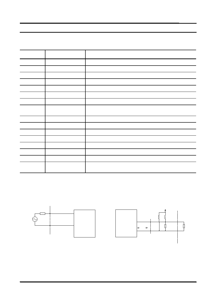
Definition of CDMA Source Impedance,
Z
S
, and AS3801 Input Impedance Z
IN
IF Signal
Source
CDMA+
Zs=1k
Zin=1k
(typ)
Vp
Vn
CDMA-
Definition of Load Impedance, Z
L
, and
AS3801 Output Impedance Z
O
TX-CDMA
Z
L
Measurement
Reference Plane
OUT+
Output
Port
OUT-
VCC
L2
R
B
L1
Z
0
ZL
eff
TX-CDMA Output Port Impedance
Z
O
>10k
Load Impedance
Z
L
=1k
Bias Resistor
R=1k
Bias Inductors
L
1
=L
2
=Choke,
.L>>R
B
Effective Load
Z
Leff
=500

Preliminary Data Sheet
AS3801
Rev. C
2/7
Nov. 98
Transfer Characteristic
-80,00
-60,00
-40,00
-20,00
0,00
20,00
40,00
60,00
0
0,5
1
1,5
2
2,5
3
3,5
Vcntrl [V]
Gain [dB]
Gain, TX 25 degC
TX, Spec
GainTX, -32degC
Gain TX, 72 degC
Intermodulation Performance
IIP3, TX AGC, 130 MHz, Vdd= 3.6V, Pin = -51 dBm
-40
-30
-20
-10
0
10
20
0
5
10
15
20
25
30
35
40
45
50
Gain [dB]
OIP3, IIP3 [dBm]
-140
-120
-100
-80
-60
-40
-20
Pim [dBm]
OIP3
IIP3
Pim