 | –≠–ª–µ–∫—Ç—Ä–æ–Ω–Ω—ã–π –∫–æ–º–ø–æ–Ω–µ–Ω—Ç: AS3802 | –°–∫–∞—á–∞—Ç—å:  PDF PDF  ZIP ZIP |
Preliminary Data Sheet
AS3802
Rev. C
1/9
Nov. 98
CDMA/FM RECEIVE AGC
AMPLIFIER AS3802
Key Features
r
Supports dual mode operation.
r
-50 to +50db gain control guaranteed.
r
Single 3.6V supply.
r
Temperature and supply stabilized.
r
Power down feature.
r
80MHz to 250MHz operation.
r
Silicon BiCMOS process.
r
Miniature surface mount 16 pin, 150 mil SSOP
package.
Compatibility
The AS3802 is designed to be functionally or/and
pin compatible to the following products:
r
RF9907
(RF Micro Devices), pin compat.
r
Q5500
(Qualcomm),
pin compat.
r
CXA3001N (Sony)
General Description
The AS3802 is a gain controlled amplifier designed
for the receive section of dual mode CDMA/FDM,
TDMA/FDM or FM/FDM cellular phones.
Key specifications like gain range noise figure, IP3,
temperature range and other specifications are
designed to be in line with the IS-95 Standard for
CDMA cellular communications.
The circuit is designed for narrow band IF
applications but can also be used in wideband
applications.
Applications
r
Digital cellular systems with receiving methods:
CDMA/FDM, TDMA/FDM, FM/FDM and
TDMA/TDD.
r
Examples: IS-95 CDMA, IS-54 DAMPS, AMPS,
PWT.
r
Cordless phones analog/digital.
r
General purpose linear IF amp's.
r
WLL / WLAN
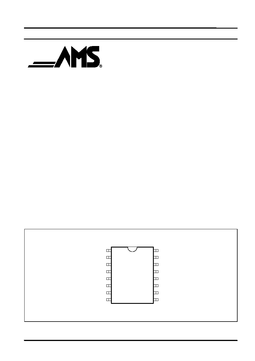
SSOP-16
CDMA+
CDMA-
GND
FM+
FM-
GND
SEL
PWD
OUT-
OUT+
GND
GND
VCC
VCC
VCC
VCTRL
1
2
3
4
5
6
7
8
16
15
14
13
12
11
10
9
AS3802
Austria Mikro Systeme International AG

Preliminary Data Sheet
AS3802
Rev. A
2/9
Jul 98
This document contains information on products under development. Austria Mikro Systeme Intl. AG reserves
the right to change or discontinue this product without notice
.
Absolut Maximum Ratings (non operating)
Symbol
Parameter
min
max
Unit
Note
VDD
Positive Supply Voltage
-0.5
7
V
GND
Analog Ground
0
0
V
Vin
Voltage at every Input Pin)
Gnd-0.5
VDD+0.5
V
Iin
Input Current
(into any pin except supply pins and
except low leakage pin)
-40
40
mA
Iin_15
Input Current into Low Leakage Pin
-25
25
mA
H
Humidity Noncondensing
1)
ESD
Electrostatic Discharge
1000
V
2)
Tstg
Storage Temperature
-55
125
deg C
Tlead
Lead Temperature
260
deg C
3)
Notes:
1) Defined DIN 40040 cond. F.
2) HBM: R=1.5kOhm, C=100pF.
Open collector outputs have less ESD protection because the protection diode to the positive supply
cannot be implemented (The output swing is higher than Vpos.+0.7V).
3) 260 deg C for 10 sec (Reflow and wave soldering), 360 deg C for 3 sec (Manual soldering).
The above figures conform to CMOS standard for low leakage application.
Recommended Operating Conditions
Symbol
Parameter
min
typ
max
Unit
Note
VDD
Positive Supply Voltage
3.6
V
1)
GND
Analog Ground
0
0
0
V
Idd
Supply Current
10
14
mA
2)
Tamb
Ambient Temperature Range,
Operating Range
-30
+80
deg C
Notes:
1) 3.6V
±
5%.
2) Measured at pin VDD, see test schematic, no signal.
Preliminary Data Sheet
AS3802
Rev. A
3/9
Jul 98
RX AGC Electrical Characteristics
Parameter
min
typ
max
Unit
Note
Frequency Range
80-250
MHz
f
-3dB
=250MHz
Maximum Gain
50
dB
V
G
=3V
Minimum Gain
-50
dB
V
G
=0.2V
Noise Figure
6.5
dB
max Gain
Input IP3
-7
-14
dBm
dBm
min Gain FM
min Gain CDMA 1)
Output CP1
-25
dBm
Gain Var. in +/-630 kHz
bandwidth centered at 85MHz
+/-0.05
dB
Gain Slope Linearity
(over any 6dB segment)
+/- 3
dB
-32 to +72 deg.C
Gain Control Voltage Range
0.2-3
V
0.2V min Gain
3.0V max Gain
ref. To GND
Gain Control Input Impedance
16
k
Current Consumption
10
14
mA
Input Resistance
1k diff.
850 sing.
CDMA
FM
Output Impedance
500
500
differential
outside
(Reff. =250
)
CDMA to FM Isolation
30
dB
Power Down Mode
2)
Notes:
Measurements refered to 85MHz.
1) Two tone measurement is used.
f
1
=86MHz; f
2
=87MHz; SEL=High for CDMA mode, SEL=Low for FM mode.
2) High
Active, Low
Power save, Input impedance
16k
.

Preliminary Data Sheet
AS3802
Rev. A
4/9
Jul 98
Pin Description
Pin#
Symbol
Function
1
CDMA+
CDMA Positive Differential Input
2
CDMA-
CDMA Negative Differential Input
3
GND
Analog Ground
4
FM+
Single Ended Analog Input
5
FM-
Analog Ground Connection (RX FM Input Reference)
6
GND
Analog Ground
7
SEL
Select, CMOS Input V
SELECT
>=3.4V, CDMA Mode Select
V
SELECT
<=0.5V, FM Mode Select
8
PWD
Power down, CMOS Input V
PWD-RX
>=3.4V, RX-AGC Active
V
PWD-RX
<=0.5V, RX-AGC Off
9
OUT-
Analog Differential Output
10
OUT+
Analog Differential Output
11
GND
Analog Ground
12
GND
Analog Ground
13
VCC
VCC Power Supply
14
VCC
VCC Power Supply
15
VCC
VCC Power Supply
16
VCTRL
Analog Control Input
VCTRL=0.2V, Low Gain Rail; VCTRL=3V, High Gain Rail

Preliminary Data Sheet
AS3802
Rev. A
5/9
Jul 98
Definition of CDMA Source Impedance,
Z
S
, and AS3802 Input Impedance Z
IN
IF Signal
Source
CDMA+
Zs=500
Zin=1k
(typ)
Vp
Vn
CDMA-
R=1k
The value of the 1k
resistor is calculated in the
matching network between the filter and the input of the
RX-APM.
Definition of FM Source Impedance, Z
S
,
and AS3802 Input Impedance Z
IN
IF Signal
Source
FM+
Zs=850
Zin=850
(typ)
Vp
Vn
FM-
(AC GND)
AC GND is defined as FM- in the package pin definition.
Definition of Load Impedance, Z
L
, and
AS3802 Output Impedance Z
O
RX-CDMA
Z
L
Measurement
Reference Plane
OUT+
Output
Port
OUT-
VCC
Z1
R
B
Z1
Z
0
ZL
eff
RX-CDMA Output Port Impedance
Z
O
>5k
Load Impedance
Z
L
=500
Bias Resistor
R
B
=500
*
Bias Inductors
L=Choke,
.L>>R
B
*
Effective Load
Z
Leff
=250
*Note:
Z
1
can be a resistor or a choke.
If it is a resistor Z
1
=R
1
=250
then R
B
is not
used.
If it is a choke,
.L>>R
B
and R
B
=500
.

Preliminary Data Sheet
AS3802
Rev. A
6/9
Jul 98
Transfer Characteristic
FM RX AGC
-80,00
-60,00
-40,00
-20,00
0,00
20,00
40,00
60,00
80,00
-
0,50
1,00
1,50
2,00
2,50
3,00
3,50
Vcntrl [V]
Gain [dB]
Gain, 25 degC
Gain, 75 degC
Gain, -35 degC
CDMA RX AGC
-80,00
-60,00
-40,00
-20,00
0,00
20,00
40,00
60,00
80,00
-
0,50
1,00
1,50
2,00
2,50
3,00
3,50
Vcntrl [V]
Gain [dB]
Gain, 25 degC
Gain, 75 degC
Gain, -35 degC

Preliminary Data Sheet
AS3802
Rev. A
7/9
Jul 98
Intermodulation Performance
RX CDMA IIP3
-55
-50
-45
-40
-35
-30
-25
-20
-15
-10
-60
-50
-40
-30
-20
-10
0
10
20
30
40
Gain [dB]
IIP [dBm]
-120
-110
-100
-90
-80
-70
-60
-50
-40
Pim [dBm]
IIP3
Pim
Pin=const. = -26 dBm Pout=const. = -41 dBm
RX FM IIP3
-50
-45
-40
-35
-30
-25
-20
-15
-10
-5
0
-60
-50
-40
-30
-20
-10
0
10
20
30
40
Gain [dB]
IIP3[dBm]
-140
-130
-120
-110
-100
-90
-80
-70
-60
-50
-40
Pim [dBm]
IIP3
Pim
Pin=const. = -26 dBm
Pout=const. = -41 dBm

Preliminary Data Sheet
AS3802
Rev. A
8/9
Jul 98
Compression Behaviour
Output CP1
35
36
37
38
39
40
41
42
43
44
-90
-80
-70
-60
-50
-40
-30
Pin [dBm]
Gain [dB]
-40
-35
-30
-25
-20
-15
-10
-5
0
Pout [dBm]
Pout, RX CDMA
Gain, RX CDMA
Gain, RX FM
Pout, RX FM
-1 dB

Preliminary Data Sheet
AS3802
Rev. A
9/9
Jul 98
Typical Application @ 85MHz
The information furnished herein by Austria Mikro Systeme International is substantially correct and accurate. However, Austria Mikro Systeme
International shall not be liable to licensee or any third party for any damages, including but not limited to personal injury, property damage, loss
of profits, loss of use, interrupt of business or indirect, special incidental or consequential damages, of any kind, in connection with or arising
out of the furnishing, performance or use of the technical data. No obligation or liability to licensee or any third party shall arise or flow out of
Austria Mikro Systeme International's rendering of technical or other services.
Austria Mikro Systeme International makes no warranty, express, statutory, implied, or by description regarding the information set forth herein
or regarding the freedom of the described devices from patent infringement. Austria Mikro Systeme International reserves the right to change
specifications and prices at any time and without notice. Therefore, prior to designing this product into a system, it is necessary to check with
Austria Mikro Systeme International for current information. This product is intended for use in normal commercial applications. Applications
requiring extended temperature range, unusual environmental requirements, or high reliability applications, such as military, medical life-
support or life-sustaining equipment are specifically not recommended without additional processing by Austria Mikro Systeme International for
each application.
Copyright @ 1998, Austria Mikro Systeme International AG, Schloþ Premst‰tten, 8141 Unterpremst‰tten, Austria. All rights reserved. The
material herein may not be reproduced, adapted, merged, translated, stored, or used without the prior written consent of the copyright owner.