 | –≠–ª–µ–∫—Ç—Ä–æ–Ω–Ω—ã–π –∫–æ–º–ø–æ–Ω–µ–Ω—Ç: AS3952 | –°–∫–∞—á–∞—Ç—å:  PDF PDF  ZIP ZIP |

Data She et CELEX AS3 952
Re vis ion N o 0.9., Ma y 20 02
Pag e 1 of 19
1.
Key Features
-
Bluetooth 1.1 compliant transceiver for the ISM band
(RF range 2400-2500MHz)
-
Complete 2.4GHZ radio and 1 MBit/s burst GFSK
Modem
-
Frequency hopping (up to 3200hops/s)
-
No external IF filters
-
High sensitivity ≠90dBm
-
On chip LNA
-
Low current consumption
-
3V power supply (2,7V ... 2,3V)
-
Low standby current consumption
-
Controllable via bidirectional BlueRF interface Rxmode
2 or 3
-
Very few external components
-
Digital RSSI
-
Programmable PA gain up to 5dBm output power. No
external power amplifier required for class 2 and 3
applications
-
Flexible master clock scheme
-
supports external clocks from 8 to 23MHz
-
or use internal crystal oscillator
-
32KHz clock supply in power down mode
-
Automatic gain control
2.
General Description
The AS3952 chip is an integrated circuit that contains the
GFSK modem and the RF-Frontend for 2.4GHz short range
Bluetooth application.
AS3952 provides a low IF receiving architecture with I/Q
filtering. In the transmit path a direct-conversion scheme is
used.
In receive direction a low power LNA with excellent noise
performance enables high sensitivities. The down
conversion to an intermediate frequency is done by two
down mixers in order to get a I/Q signal. The required
synthesizer is on chip and can be fully programmed.
The IF section contains polyphase bandpass filters, VGAs,
A/D-converters and a digital GFSK demodulation circuitry.
In the transmit path there is a GFSK modulator, D/A-
converters, lowpass filters and a master interface. The I/Q
baseband signal is directly mixed to 2.4GHz. The transmit
power can be programmed up to 5dbm.
The clocking scheme of AS3952 supports many different
modes in order to fit to several baseband processor types.
AS3952 can generate master clocks or can be clocked with
an external master clock as well.
In power down mode the radio can supply either an 32KHz
or a 16MHz clock to the baseband.
3.
Applications
-
Shortrange Bluetooth wireless connection
-
WLAN FHSS modem
-
2.4GHz Data link connections
Bluetooth Radio Chip CELEX
AS3952
PRELIMINARY DATA SHEET

Data She et CELEX AS3 952
Re vis ion N o 0.9., Ma y 20 02
Pag e 2 of 19
4.
Blockdiagram
Figure 1 : Block Diagram of CELEX, AS3952, D esc ription
Polyphase filter and AGC
ADC
ADC
DAC
DAC
Synthesizer
Master
Interface
GFSK
Demodulator
GFSK
Modulator
Lowpass
RX Data
Blue RF
TX Data
BW=1MHz
PA
LNA
Down Converter
Up Converter
I
Q
I
Q
Low/High Gain
RF In
RF Out
RFControl
Unit
L
N
A
c
o
n
t
r
o
l
P
o
w
e
r
C
o
n
t
r
o
l
G
a
i
n
S
e
l
e
c
t
AGC Control
RXIP
RXIN
RXQP
RXQN
REF_CLK
TXIP
TXQP
DA
T A
G_SEL
TXIN
TXQN
3
1
2
TX_ON
1
L
e
v
e
l
D
e
t
e
c
t
LEV_DET
POR
XOSC
MCLK
VCO_CLK
PA_PWON
P
o
w
e
r
O
n

Data She et CELEX AS3 952
Re vis ion N o 0.9., Ma y 20 02
Pag e 3 of 19
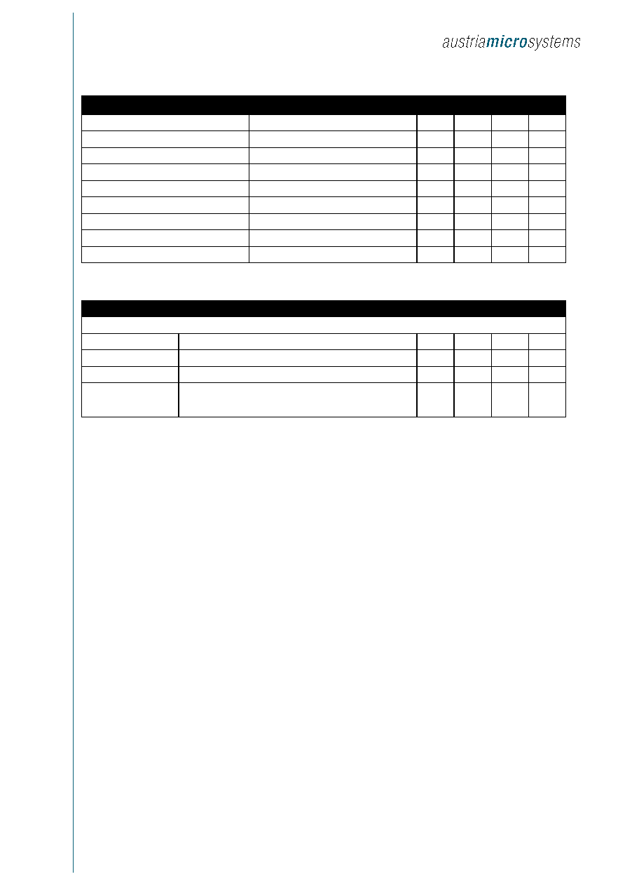
4.1
System Specification
Parameter
Description
Min
Typ
Max
Units
Transmit Power
measured at the antenna port
-5
0
5
dBm
Adjacent channel power
@ ± 500kHz
-20
dBc
Adjacent channel @ 2MHz
Sum of power in a 1MHz bandwidth
-20
dBm
Adjacent channel @
3MHz
Sum of power in a 1MHz bandwidth
-40
dBm
30MHz-1GHz
-57
dBm
1GHz ≠12.75GHz
-47
dBm
1.8GHz ≠ 1.9GHz
-47
dBm
Out of band power (idle
mode)
5.15GHz ≠ 5.3GHz
-47
dBm
30MHz-1GHz
-36
dBm
1GHz ≠12.75GHz
-30
dBm
1.8GHz ≠ 1.9GHz
-47
dBm
Out of band power
(operating mode)
5.15GHz ≠ 5.3GHz
-47
dBm
Initial carrier frequency
tolerance
30ppm
± 75
kHz
Frequency drift rate
400
Hz/µ s
Frequency drift
during 625µ s
± 25
kHz
during 1875µ s
± 40
kHz
during 3125µ s
± 40
kHz
Table 1: Transmit Syste m Char acte ristics
Parameter
1
Conditions
Min
Typ
Max
Units
Sensitivity
@ BER
0.1%
- 90
dBm
Usable level
@ BER
0.1%
-20
dBm
IIP3
-10
dBm
Co-channel interference
C=-60dBm
11 (14)
dB
Adjacent interference C/I
C=-60dBm @ 1MHz
0 (4)
dB
Adjacent interference C/I
C=-60dBm @ 2MHz
-30
dB
Adjacent interference C/I
C=-67dBm@
3MHz
-40
dB
Image interference, C/I
Ima ge
C=-67dBm
-9 (-6)
dB
Spurious emissions @ 100kHz bandwidth
30MHz ≠ 1GHz
-57
dBm
Spurious emissions @ 100kHz bandwidth
1GHz ≠ 12.75GHz
-47
dBm
RSSI golden receive range
± 4
dB
RSSI range lower limit
-84
-56
dBm
1
Values in brackets are from the "Bluetooth Specification 1.0" for a convergence period of three years.
Data She et CELEX AS3 952
Re vis ion N o 0.9., Ma y 20 02
Pag e 4 of 19
Parameter
1
Conditions
Min
Typ
Max
Units
RSSI range upper limit
Starting at lower limit
20± 6
dB
Intermodulation characteristics
tbd.
Out of band blocking
30MHz ≠2000MHz
-10
dBm
2000MHz ≠ 2399MHz
-27
dBm
2498MHz ≠ 3000MHz
-27
dBm
3000MHz ≠ 12.75GHz
-10
dBm
Spurious emissions
100kHz bandwidth
30MHz ≠ 1GHz
-57
dBm
1GHz ≠ 12.75GHz
-47
dBm
Table 2: Receiv e Syst em Cha ract eristic s
Parameter
Description
Min
Typ
Max
Units
GFSK, BT=0.5
Deviation
modulation index 0.32
± 160
kHz
Minimal deviation
± 115
kHz
Symbol timing
± 20
ppm
Deviation
ratio=
f2/f1
f2 corresponds to 10101010 bit stream
f1 corresponds to 00001111 bit stream
0.8
Table 3 Modem Charact eristic s
Data She et CELEX AS3 952
Re vis ion N o 0.9., Ma y 20 02
Pag e 5 of 19
5.
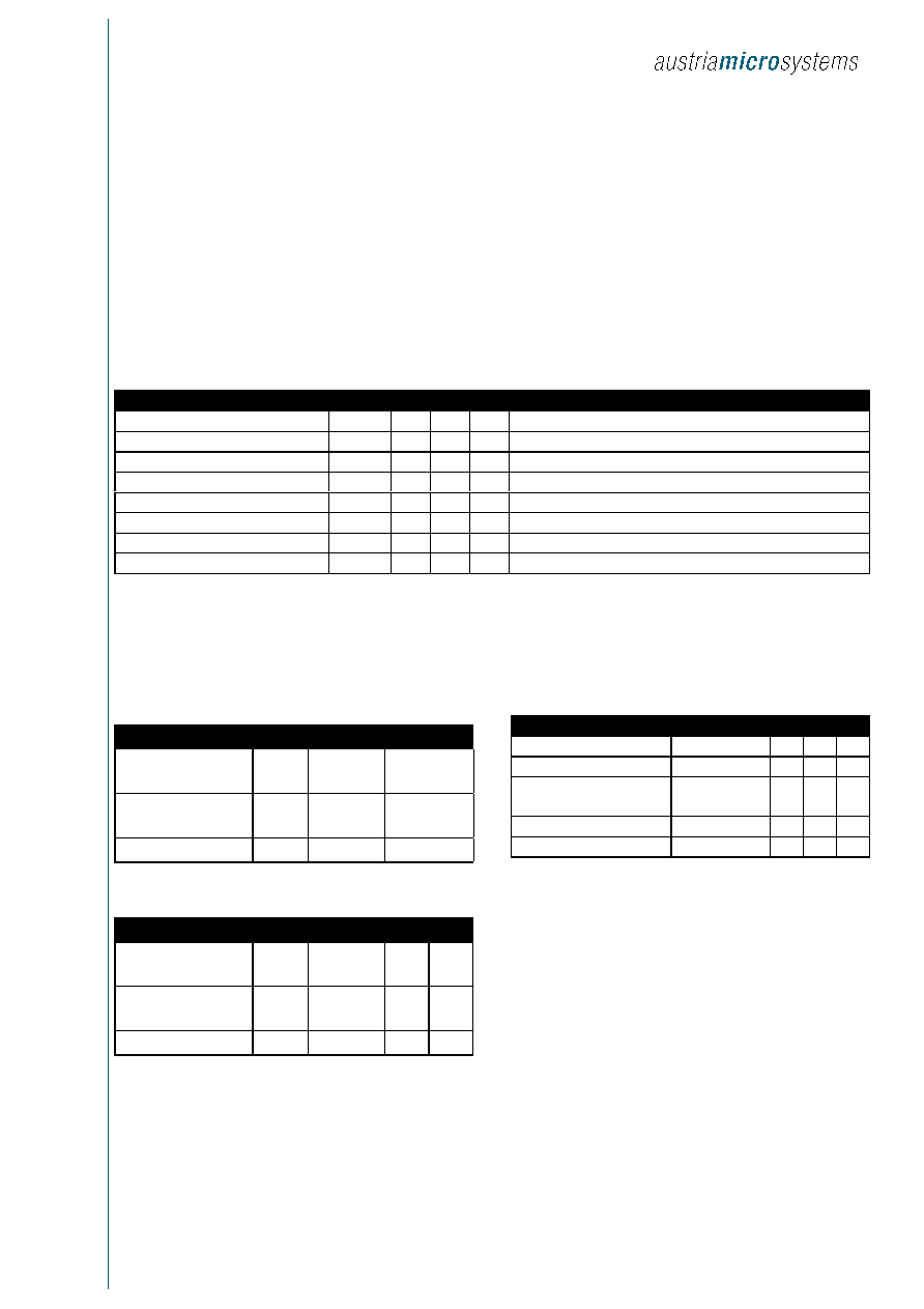
General Device Specifications
5.1
Absolute Maximum Ratings (non
operating)
Stresses beyond those listed under "Absolute Maximum
Ratings" may cause permanent damage to the device.
These are stress ratings only. Functional
operation of the device at these or any other conditions
beyond those indicated under "Operating Conditions" is not
implied. Exposure to absolute maximum rating conditions
for extended periods may affect device reliability.
Parameter
Symbol
Min
Max
Unit Note
Analog supply
AVDD
-0.7
6
V
Digital supply
DVDD
-0,7
6
V
Input current (latch-up immunity)
I
SCR
-40
40
mA
Norm: Jedec 17
ESD (standard pads)
±1
kV
Norm: MIL 883 E method 3015
ESD (RF pads)
±0.5
kV
Norm: MIL 883 E method 3015
Storage temperature
T
STRG
-55
125
O
C
Soldering conditions
T
LEAD
Norm: EC 61760-1
Humidity
5
85
%
Non-condensing
Table 4: Absolute maximum ratings (non operating)
5.2
DC/AC Characteristics for Digital
Inputs and Outputs
Parameter
Symbol
Min
Max
Unit
High level input
voltage
VIH
0.7 * DVDD
V
Low level input
voltage
VIL
0.3 *
DVDD
V
Input leakage current
ILEAK
1
µ A
Table 5: CMOS Input level
Parameter
Symbol
Min
Max
Unit
High level output
voltage
VOH
DVDD-0.5
V
Low level output
voltage
VOL
DVSS
+0.4
V
Capacitive load
CL
20
pF
Table 6: CMOS Output level
5.3
Operating Conditions
Parameter
Symbol
Min Max Unit
Positive supply Voltage
AVDD
2.7
3.3
V
Negative supply Voltage
0
0
V
Difference AVDD - DVDD
AVDD-DVDD and
AVSS-DVSS
-0.1
0.1
V
Digital supply Voltage
DVDD-DVSS
2.7
3.3
V
Ambient temperature
T
AMB
-30
85
O
C
Table 7: Operating Conditions

Data She et CELEX AS3 952
Re vis ion N o 0.9., Ma y 20 02
Pag e 6 of 19
5.4
Clock Scheme
In order to fit to several baseband processors AS3952
supports a flexible clocking scheme. AS3952 is capable to
either generate its own clock or to handle different external
clocks.
5.4.1
Crystal oscillator
In this mode AS3952 can be used as a clock supply for a
whole Bluetooth Application. AS3952 has its own crystal
(16MHz) and supplies a master clock MCLK to the
baseband. During DEEP SLEEP mode an internal divider
provides a 32kHz signal at the MCLK pad. The 32kHz signal
can be used by the baseband in power down mode to clock
a wake-up timer.
5.4.2
External clock
AS3952 supports the use of external frequencies between 8
and 23MHz in 1MHz steps. In this mode the internal crystal
oscillator is disabled. An internal PLL circuit generates the
required 16MHz clock.
5.5
Power Down Concepts
The power down is controlled via registers, were the
settings of the power down pins are stored. In IDLE mode
the analog part is set into power down according the
settings of this register.
Mode
Entered
Description
OFF
RESET=1 or BnPWR=0
16MHz are provided, all register settings are set to default
SLEEP
BXTLEN=0 and LOW_CLK =0
All programming is maintained. 16MHz is provided on MCLK
DEEP SLEEP
BXTLEN=0 and LOW_CLK =1
All programming is maintained. 32kHz is provided on MCLK
Table 8: Power down concepts and mode description
5.6
IF Receive Section
The bandpass polyphase filter provides the channel
selectivity and mirror suppression. Due to noise reduction
the BPs and VGAs are interleaved.
5.6.1
Offset Calibration
The Offset of each AGC stage is cancelled in order to avoid
signal clipping. The algorithm is implemented in the modem
and runs fully automatically. The baseband starts the offset
calibration either during initial programming or before
transmission of a package.
5.6.2
Digitally Controlled Gain Amplifier
The variable gain amplifier adjusts the amplitude of the IF
signal in order to exploit the full input range of the
succeeding analog-to-digital converter. The amplifiers are
controlled by a digital algorithm which calculates the level
of the signal by using the I and Q channel. Depending on
the signal strength the gains are set fully automatically.
6.
Master Interface (Blue-RF based)
6.1.1
Introduction
The bi-directional mode provides the lowest pin count
interface between the baseband and CELEX AS3052. It
supports RXMODE 2 and 3. The control of CELEX is done
via a DBus control interface.
State machines in the baseband and the radio maintain the
state which controls the direction of the three bi-directional
pads. The baseband controls the state machine in the radio,
and ensures data contentions do not occur during reset and
normal operation.
Data interface:
BDATA1
BlueRF data signals
BPKTCTL
BlueRF PA enable signal
BXTLEN
BlueRF XTAL enable signal
BnPWR
BlueRF power down signal
BRCLK
BlueRF clock signal 1, 8 or 16MHz
MCLK
Master clock 16MHz or 32kHz

Data She et CELEX AS3 952
Re vis ion N o 0.9., Ma y 20 02
Pag e 7 of 19
Figure 2: Signals of data and control interface
Control interface (DBus):
BDATA1
Data transmission
BDCLK
Serial clock from baseband
BnDEN
Data enable signal from the baseband
It is possible to derive all bi-directional timing from BRCLK,
except for the power-up sequence.
∑ The radio always uses the negative edge of BRCLK
∑ The baseband uses the positive edge of BRCLK.
6.1.2
Power-Up Sequence
When BnPWR is Low, it holds the radio in the OFF state
where:
∑
analogue and digital blocks are powered down
∑
all configuration data is lost.
∑
16MHz clock is provided
When BnPWR and BXTLEN are driven High the radio moves
from the OFF State to the IDLE state.
Figure 3: Power up sequence
Ba
se
ba
nd
CEL
E
X
AS
3952
BnDEN
BDCLK
BDDATA
BnPWR
BRCLK (1, 8 or 16MHz)
BXTLEN
BPKTCTL
BDATA1
BnPWR
BXTLEN
BDATA1
BRCLK
DBus
Write/Read Registers
OFF
IDLE
16 MHz

Data She et CELEX AS3 952
Re vis ion N o 0.9., Ma y 20 02
Pag e 8 of 19
Figure 4: State diagram BlueRF interfac e (actions of the DBus interfac e ar e ma rked in blue).
State
Description
OFF
Lowest power state (all control register are set to default values).
IDLE
Radio oscillator enabled and settled, and BDATA1 may change state
SLEEP
32kHz low power clock or 16MHz is provided on MCLK depending on Bit LOW_CLK
Table 9: Bi-d irection a l p ower- up state d escri ptio n
OFF
IDLE
SLEEP
WAIT
DATA SYNC
DATA SYNC
ENABLE PA
TX DATA
DISABLE PA
RX PLL WAIT
RX WIDE FILT
BnPWR=0
BXTLEN=1
BnPWR=1
BXTLEN=1
BDATA1=1
BPKTCTL=1
Write Config
Write
- Hopping Freq
-PLL enable
-Enable TX
PA is ready to
transmit
BPKTCTL=0
Write
Control
IDLE
Write
- Hopping Freq
- PLL enable
- Enable RX
Radio is ready
to receive
RX NARROW
FILT
Write
Control
IDLE
BPKTCTL=1
BPKTCTL=0
BXTLEN=0

Data She et CELEX AS3 952
Re vis ion N o 0.9., Ma y 20 02
Pag e 9 of 19
6.1.3
Power Mode SLEEP
The radio is in the IDLE state when in use after following
the power-up sequence. One other low power state is
defined for the bi-directional interface, SLEEP. In the
SLEEP state, the crystal oscillator can either be disabled or
enabled. All the analogue blocks are held in the lowest
power state, but unlike the LOW POWER state, all the
configuration register data is retained.
When the crystal oscillator is enabled it can be programmed
with the LOW_CLK bit to supply either 16 MHz or 32Khz.
The baseband can drive the radio into the SLEEP state by
driving BXTLEN Low at any time from any state, except
OFF.
6.1.4
Transmit Mode
There are five states through which baseband drives the
radio to transmit data. The transitions through these states
are illustrated in figure 4.
The radio only provides the BRCLK which will be 16MHz. In
transmit mode, data is transferred across the data interface
at a 1MHz rate. The radio is able to generate an
unmodulated carrier before the real data is transmitted. The
duration of the unmodulated carrier is programmable.
6.1.5
Transmit Data Synchronization
It is required that the radio must synchronize transmit data
with the baseband before the transmit power amplifier (PA)
is enabled.
The radio achieves transmit data synchronization by the
baseband providing at least one transition on BDATA1 n*µ s
(T
SY NC
, where n is an integer) before the time data is
required to be transmitted on air. Synchronization is only
possible whilst BPKTCTL is driven low by the baseband.
The baseband derives an internal transmit clock (TXCLK)
which has a rate equal to the symbol rate (T
SY MB OL
) by
dividing down BRCLK.
Following a transition on BDATA1, the radio initiates a
sampling clock with a period of T
SY MB OL
, and an offset from
the transition on BDATA1 by the period T
PHYSAMP
(which
approximately equals one half T
SY MB OL
).
Figure 5: Transmit d ata synchr on izati on
6.1.6
Data Transmit States
The five states related to data transmission are:
State
Description
WAIT DATA
SYNC
Transmit mode has been enabled by
setting the appropriate registers in the
radio. Transmit data transfer has not
been synchronized between the
baseband and radio.
DATA SYNC
Transmit data transfer is being
synchronized between the baseband and
radio initiated by the rising edge of
BDATA1. The internal sampling clock of
the radio is adjusted to the middle of a
symbol (T
PHYSAMP
Offset).
ENABLE PA
This state is entered when the baseband
drives BPKTCTL High. The PA_EN_Timer
is started and after the time T
P A
an
unmodulated carrier is sent.
TX DATA
This state is entered when the
PA_EN_Timer is zero. The radio remains
in this state until all the data has been
transmitted.
DISABLE PA
This state is entered when BPKTCTL is
driven Low and the PA is powered down.
The state is exited by the baseband
writing to the appropriate registers in the
radio after a fixed settling time.
Table 10: Transmit mod e states
BRCLK
(16MHz)
BDATA1
Baseband
TXCLK
Sampling CLK
T
PHY SAM P
T
SY M BOL

Data She et CELEX AS3 952
Re vis ion N o 0.9., Ma y 20 02
Pag e 10 of 19
WAIT DATA SYNC is entered from the IDLE state by a
control register write, which transfers all the information
required by the radio to enable the transmit path. Before
data can be transmitted on air, the transmit data timing on
the BlueRF interface needs to be synchronized, as
described in the previous section. The synchronization
takes place in the DATA SYNC state.
Note: DATA SYNC can start before the hop frequency
generator locks onto frequency.
When the radio is synchronized the radios PA amplifier is
enabled by the baseband driving BPKTCTL High and the
ENABLE PA state is entered. An internal timer is set with
the programmable value (PA_EN_TIMER) and after the time
has elapsed the modulator is switched to the antenna and
the TX state is entered. The data must be applied on the
BDATA1 signal after T
UNC
. therefore it is recommended to
use multiples of the symbol period.
The PA_EN_Timer can be set to any value between 0 and
255, which corresponds to multiples of 16MHz periods. The
following formula should be used to calculate the right
value.
PA_EN_Timer = T
UNC
+ T
TX D
= n*16 + 51
n... is an integer, that gives the time in µ s between the
rising edge of BPKTCTL and the start of the first data bit
Basically T
UNC
can be set to any value in steps of 16MHz
periods. But it is recommended to use multiples of 1µ s
(16*n).
Data is transmitted until the DISABLE PA state is entered
by the baseband driving BPKTCTL low. After the settling
time the baseband enters IDLE state by a control register
write.
Figure 6: Timing d iag ram of d ata transmissio n
IDLE
RF Data
. . .
. . .
IDLE
WAIT DATA
SYNC
DATA
SYNC
ENA. PA
TX DATA
DIS.
PA
T
TX D
T
TX D
T
DPA
T
P A
T
SY NC
= n * 1µ s
DBus
Signal on
Air
BDATA1
BPKTCTL
TXCLK
1MHz
un mod ul ated
PA_En_Timer
T
UNC

Data She et CELEX AS3 952
Re vis ion N o 0.9., Ma y 20 02
Pag e 11 of 19
6.1.7
Data Interface Timing Transmit
Symbol
Parameter
Min
Typ
Max
Unit
T
SY MB OL
Time to transmit a single Symbol
1
µ s
T
PHYSAM
P
Synchronization Delay
0.5
µ s
T
X TL
Time from entering PWRON WAIT XTL to crystal oscillator becoming stable.
15
ms
T
X TLHOLD
min. Time from entering state HOLD XTL till going to IDLE
1
µ s
T
TX D
Delay through of the modulator (= 51*62,5ns)
3,1875
µ s
T
P A
Time to switch on Power Amplifier
<10
ns
T
DPA
Time to switch off Power Amplifier
<10
ns
T
UNC
Time of unmodulated Carrier. Programmable in steps of 62,5ns.
Multiple of 16*n (1µ s) is recommended.
n*µ s
T
SY NC
This time is an integer of n and is given by the baseband
n*µ s
Table 11: Data Interf ace Timing Transmit
6.1.8
Receive Mode RXMODE-2
The RXMODE2 mode describes the system partitioning
where the radio contains the demodulator and the DC
estimator. The data extraction must be done in the
baseband. The table below shows data direction and signal
usage.
Pad RX
Direction
Description
Function
BDATA1
Radio
Õ Baseband Receive data
BPKTCTL
Baseband
Õ Radio
Control of RX NARROW
FILT mode
BXTLEN
Baseband
Õ Radio Crystal oscillator enable
BRCLK
Radio
Õ Baseband Data sample clock
Table 12: Data d irectio n and sig na l usag e
State
Description
RX PLL WAIT
Baseband waits for a fixed length of time
for the hop frequency synthesizer to
settle.
RX WIDE
FILT
The baseband enters this state when the
hop frequency synthesizer has settled.
The baseband receives data and searches
for the access code.
RX NARROW
FILT
The demodulation algorithm is set to a
slower time constant
Table 13: Rece i ve RXMODE 2 states
From the IDLE state, RX PLL WAIT state is entered by the
baseband writing to the appropriate control registers in the
radio. During RX PLL WAIT, the direction of BDATA1
changes from being driven by the baseband to being driven
by the radio. After the hop frequency generator settling
period T
SY NT
, the RX WIDE FILT state is entered and the
baseband starts to interpret the received data.
6.1.9
Bi-directional Turn Round Time
The signal BPKTCTL is driven High by the baseband to
make the radio to enter the RX NARROW FILT state. The
bi-directional interface is placed back in the IDLE state by
the baseband writing the relevant radio control registers.
The bi-directional BlueRF link enters the IDLE state.
During the clock period after the radio's control register is
updated, BDATA1 reverts back to being driven by the
baseband
The signal BDATA1 changes from being driven by the
baseband to being driven by the radio on entering the
receive mode, and back to being driven by the baseband
on exiting the receive mode. The baseband stops driving
the signal just before the DBus command for receive (RX)
becomes valid in the radio, and the radio drives the signal
immediately the RX command becomes valid.
On leaving the receive state, the radio stops driving
BDATA1 as soon as the DBus command to enter the idle
state becomes valid.

Data She et CELEX AS3 952
Re vis ion N o 0.9., Ma y 20 02
Pag e 12 of 19
Figure 7:Timing d iag ram of d ata reception i n RXMODE 2
6.1.10
Receive Mode RXMODE 3
AS3952 also provides the RXMODE 3 where the access
code is also detected by the modem. The appropriate
access code must be programmed via the DBus interface.
The data interface with the signals is shown in figure 8.
Figure 8 Sig nal s etting s of the d ata interface i n RXMODE 3
State
Description
FIND
ACCESS
CODE
This state is entered via a command at
the DBus interface. AS3952 correlates
the programmed access code with the
received data.
RX BIT DATA
This state is entered after AS3952 has
State
Description
received the right access code. Receive
data is now transferred to the baseband
on BDATA1. AS3952 indicates to the
baseband that this state has been
entered by driving the BPKTCTL to
High.
Table 14 Rece i ve RXMODE 3 states
From the RX PLL WAIT state, FIND ACCESS CODE state is
entered by the baseband writing to the appropriate control
registers to AS3952. When the FIND ACCESS CODE state
is entered, BDATA1 and BPKTCTL change direction and
become driven by the AS3952. The AS3952 now performs
all of the tasks required to correlate with the access code
and extract the receive data. When the AS3952 has
correlated the access code, and it has data which is ready
to be sent to the baseband, it raises the BPKTCTL.
The baseband samples the RX data with a period T
SAMP LE
with an offset of one half T
SAMP LE
from the time the AS3952
drives
The bi-directional interface is placed back in the IDLE state
by the baseband writing the relevant AS3952 commands to
the control registers. During the clock period after the PHY
control register is updated, BDATA1 and BPKTCTL revert
back to being driven by the baseband.
Ba
se
ba
nd
CEL
E
X
AS
3952
Data
DBus
BnDEN
BDCLK
BDDATA
BRCLK (1MHz)
BXTLEN
BPKTCTL
BDATA1
...
...
IDLE
RX PLL WAIT
RX WIDE FILT
IDLE
T
TAR
T
SY NT
T
RXD
Signal on
Air
DBus
BDATA1
BRCLK
(8MHz)
RF Data
T
TAR
BPKTCTL
RX NARROW FILT
16MHz
16MHz

Data She et CELEX AS3 952
Re vis ion N o 0.9., Ma y 20 02
Pag e 13 of 19
Fig ure 9: Timing d iag ram of d ata reception i n RXMODE 3
Symbol
Parameter
Min
Typ
Max
Unit
T
SY MB OL
Time to transmit a single Symbol
1
µ s
T
PHYSAM
P
Synchronization Delay
0.5
µ s
T
TAR
Bi-directional turn around time
20
µ s
T
SY NT
Time between hop frequency programming to synthesizer stabilizing
140
µ s
T
ACC
Time to correlate the access Code
72
µ s
T
RXD
Delay through the radio from the antenna
tbd.
Table 15: Data interf ace timing rec eive
IDLE
RX PLL WAIT
FIND ACCESS CODE
IDLE
T
TAR
T
SY NT
T
RXD
Signal on Air
DBus
BDATA1
BRCLK
(1MHz)
RF Data
T
TAR
BPKTCTL
RX BIT DATA
T
ACC

Data She et CELEX AS3 952
Re vis ion N o 0.9., Ma y 20 02
Pag e 14 of 19
6.2
The DBus Protocol
6.2.1
Introduction
The radio is programmed with control data via the three wire
serial Interface (DBus). The baseband is always the DBus
master and therefore initiates all accesses. There are three
signals used for the DBus interface:
BDDATA Bi-directional signal for Data Transmission
BDCLK Serial Clock from baseband
BnDEN Data enable Signal (Active Low)
The DBus protocol consists of the following sections:
∑ the device address
∑ read/write access control
∑ the register address
∑ the data field.
Field
Bit
count
Comment
Device
address
3
The radio is allocated device
address "101" binary.
Read /
write
1
H=Read; L=Write
Register
address
5
Register Address
Data field
16
Driven by the baseband for write,
the radio for read
Table 16: DBus prot oco l d ata p acket spec ificati on
Initially, the clock line (BDCLK) is driven low. The active low
enable strobe (BnDEN) is driven low by half a BDCLK clock
cycle before the first active, positive BDCLK edge, which
allows clean clock gating. At the first rising BDCLK edge,
the MSB of the address is clocked into the radio via the
data signal (BDDATA). The DBus protocol requires that the
addressed slave device either reads or writes data on the
rising edge of a clock pulse.
The default is that the DBus master is responsible for
driving all three of the interface signals (BDDATA, BDCLK
and BnDEN) except for a read access where it releases the
BDDATA line to be driven by the addressed slave
peripheral.
6.2.2
DBus Write
The DBus master will drive out new data on the falling edge
of BDCLK. All four DBus data fields are transferred from the
baseband to the radio with the same timing. Following the
last data bit, the baseband drives the enable line (BnDEN)
High for a minimum of two BDCLK periods to indicate the
arrival of the final data bit, and enable data transfer from
radio's shift register to the data register. The radio uses the
positive edge of the last clock pulse with BnDEN High to
update the data register with the shift register content.
Figure 10: Write pr oced ure o n DBus
1
0
1
A4
A3 A2
A1
A0
D15 D14 D13 D12 D11 D10 ....
D2
D1
D0
Don't Care
BnDEN
BDDATA
BDCLK
WRITE

Data She et CELEX AS3 952
Re vis ion N o 0.9., Ma y 20 02
Pag e 15 of 19
6.2.3
DBus Read
During a read access, the radio generates data to be read
by the baseband. Following the transfer of the address and
read / write control fields by the baseband, there is a turn
round bit lasting half a clock cycle. It has the effect of
realigning the DBus timing such that the radio will drive its
data onto BDDATA on the rising edges of BDCLK. The DBus
master reads input data on BDDATA on either the falling or
rising edges of BDCLK. Following the transfer of the last
data bit, D[0], BDDATA reverts to being driven by the
master. The slave stops driving BDDATA on the rising edge
and the master resumes driving on the falling edge of the
first BDCLK pulse after BnDEN is driven High.
The DBus protocol requires that BDDATA be driven by the
baseband whilst it is providing address and control
information, the bus direction then turns round, and the
radio drives BDDATA to provide the read data. During the
turn round period, the baseband stops driving BDDATA on a
negative edge of BDCLK, and the radio starts driving
DBDATA on the subsequent rising edge of BDCLK. The
baseband requests that the radio stops transmitting data by
driving BnDEN High. BnDEN changes on a falling edge of
BDCLK, on the subsequent rising edge, the radio stops
driving BDDATA, and on the next subsequent falling edge,
the baseband resumes driving BDDATA.
Figure 11: Read access o n Dbus
6.2.4
DBus Read Timing Loop
BDCLK is driven by the baseband, and is used by the radio to clock read data back to the baseband.
Parameter
Min
Max
Comment
T
MZ
8ns
5ns
Time for the baseband to go from driving BDDATA to going tri-state.
T
MD
-5ns
20ns
Time for the baseband to go from tri-state to driving BDDATA
T
SZ
0ns
15ns
Time for the radio to go from driving BDDATA to going tri-state.
T
SDV
0ns
15ns
Time for the radio data to become valid from the rising clock edge.
T
SD
0ns
15ns
Time for the radio to go from tri-state to driving BDDATA (note less than or equal to TSDV)
Table 17: Dbus timing read loop
1
0
1
A4
A3 A2
A1
A0
D15 D14 D13 D12 D11 ....
D2
D1
D0
Don't Care
BnDEN
BDDATA
BDCLK
READ
floating
floating

Data She et CELEX AS3 952
Re vis ion N o 0.9., Ma y 20 02
Pag e 16 of 19
6.2.5
DBus Timing
Serial interface DBus timing
Parameter
Symbol
Min
Max
Unit
Conditions
BDCLK, clock
frequency
F
CLOCK
-
20
MHz
BDCLK low
pulse duration
T
CL,min
25
ns
The minimum time BDCLK must be low.
BDCLK high
pulse duration
T
CH,mi n
25
ns
The minimum time BDCLK must be high.
BnDEN setup
time
T
SA
2
-
ns
The minimum time BnDEN must be low before positive edge of
BDCLK.
BnDEN hold
time
T
HA
2
-
ns
The minimum time BnDEN must be held low after the positive edge
of BDCLK.
BDDATA setup
time
T
SD
2
-
ns
The minimum time data on BDDATA must be ready before the
positive edge of BDCLK.
BDDATA hold
time
T
HD
2
-
ns
The minimum time data must be held at BDDATA, after the positive
edge of BDCLK.
BDDATA output
delay
T
SDV
16.2
-
ns
The maximum time before data on BDDATA is valid after the
positive edge of BDCLK.
Rise time
T
rise
100
ns
The maximum rise time for BDCLK and BnDEN
Fall time
T
fall
100
ns
The maximum fall time for BDCLK and BnDEN
Notes:
The set-up- and hold-times refer to 50% of VDD.
Output delays are for 50pF load on output.
T
HA
T
SA
T
SD
T
HD
T
SDV
Write Data
Read Data
BDCLK
BnDEN
BDDATA

Data She et CELEX AS3 952
Re vis ion N o 0.9., Ma y 20 02
Pag e 17 of 19
7.
Register Description
A description of the register contents for each register in given in the Programming Guide.
8.
Package and Marking
8.1
Pin Description AS3952 Chip
Pin Name
Type Description
Section
1
VCCBIAS
S
Positive supply
RF
2
VCCLNA
S
Positive supply
RF
3
GNDTXRX
S
Negative supply
RF
4
LNAIN
RF
Low noise amplifier input
RF
5
GNDTXRX
S
Negative supply
RF
6
PAOUT
RF
Power amplifier output
RF
7
GNDTXRX
S
Negative supply
RF
8
VCCPA
S
Positive supply
RF
9
GNDMIX
S
Negative supply
RF
10 VCCMIX
S
Positive supply
RF
11 VEEECL
S
Negative supply
RF
12 VCCECL
S
Positive supply
RF
13
TXON
DO
Transmit-on signal (to TX/RX switch and external PA if used)
RF
14
VEECHP
S
Negative supply
RF
15
VCCCHP
S
Positive supply
RF
16
VDD_LPF_RX2
VDD_BIAS_RX1
S
Positive supply
IF
17
GND_LPF_RX2
GND_BIAS_RX1
S
Negative supply
IF
18
VDDA_TG
A
Analog test pin
IF
19
GND_DAC_ADC
GND_REF
S
Negative supply
IF
20
VDD_DAC_ADC
VDD_REF
S
Positive supply
IF
21 ADC_VREF
A
Reference voltage of ADC (external capacitor connected)
IF
22
NC
IF
23
BPKTCTL
DIO
Enable power amplifier (I)
Radio decoded access code (O)
IF
24
BXTLEN
DIO Enable oscillator / reset strobe input (output in test mode)
IF

Data She et CELEX AS3 952
Re vis ion N o 0.9., Ma y 20 02
Pag e 18 of 19
Pin Name
Type Description
Section
25
MCLK
DO
Master clock 16MHz or 32kHz in "DEEP SLEEP" mode
IF
26
BDATA1
DIO RF data input / output
IF
27
BRCLK
DO
RF data path clock (16MHz in transmit, 1MHz in receive)
IF
28
BnDEN
DI
DBus serial interface, data strobe (active low)
IF
29
BDCLK
DI
DBus serial interface, clock
IF
30
BDDATA
DIO DBus serial interface, data input/output
IF
31
BnPWR
DI
Low power state enable input (active low)
IF
32
RESET
DO
Power on reset output (active high)
IF
33
DSUB
S
Substrate ground connection of digital cells
IF
34
VDD_DIG
VDD_OSC
S
Positive supply
IF
35
XOSC_Q2
A
Crystal, pin 2 (16MHz XTAL connection)
IF
36
XOSC_Q1
A
Crystal, pin 1, also used for external clock input (16MHz XTAL connection or
6...20MHz input)
IF
37
VSS_OSC
VSS_DIG
S
Negative supply
IF
38
PAD_WR_N_Q
A
Analog test pin
IF
39
RBIAS
A
Connection for external precision resistor
IF
40
PAD_WR_P_Q
A
Analog test pin
IF
41
ICP
A
Charge pump output to external loop filter (if used)
RF
42
VCCVCO
S
Positive supply
RF
43
GNDVCO
S
Negative supply
RF
44
GNDBIAS
S
Negative supply
RF
PIN Types:
S
...
supply pad
A
...
analog pad
RF
...
special RF pad
DI
...
digital input pad
DO
...
digital output pad
DIO
...
digital input/output pad
8.2
Marking / Package (preliminary)
Production Parts
Package type
to be defined

Data She et CELEX AS3 952
Re vis ion N o 0.9., Ma y 20 02
Pag e 19 of 19
Headquarters
austriamicrosystems AG
accento!
Business Unit Communications
A 8141 Schloss Premst‰tten, Austria
T. +43 (0) 3136 500 0
F. +43 (0) 3136 525 01
accento@austriamicrosystems.com
www.austriamicrosystems.com
Sales Offices
Germany
austriamicrosystems Germany GmbH
Tegernseer Landstrasse 85
D-81539 M¸nchen, Germany
Phone: +49/89/693643-0
Fax: +49/89/693643-66
France
austriamicrosystems France S.a.r.l.
124, Avenue de Paris
F-94300 Vincennes, France
Phone: +33/1/43 74 00 90
Fax: +33/1/43 74 20 98
Italy
austriamicrosystems Italy S.r.l.
Via Leone Tolstoi, 64
I-20146 Milano, Italy
Phone: +39/0242/36713
Fax: +39/0242/290889
Switzerland
austriamicrosystems Switzerland AG
Rietstrasse 4
CH-8640 Rapperswil, Switzerland
Phone: +41/55/220 9000
Fax: +41/55/220 9001
USA (west)
austriamicrosystems USA, Inc.
Suite 116, 4030 Moorpark Ave,
San Jose, CA 95117, USA
Phone: +1/408/345 1790
Fax: +1/408/345 1795
USA (east)
austriamicrosystems USA, Inc.
Suite 400, 8601 Six Forks Road
Raleigh, NC 27615, USA
Phone: +1/919/676 5292
Fax: +1/919/676 5305
United Kingdom
austriamicrosystems UK, Ltd.
Coliseum Business Centre, Watchmoor Park
Camberley, Surrey, GU15 3YL, UK
Phone: +44/1276/23 3 99
Fax: +44/1276/29 3 53
Japan
austriamicrosystems AG
Shin Yokohama Daini, Center Bldg. 10F
3-19-5, Shin Yokohama
Kohoku-ku, Yokohama 222-0033, Japan
Phone: +81/45/474 0962
Fax: +81/45/472 9845
Distributors & Representatives
austriamicrosystems AG is represented by distributors in
the following countries. Please contact your nearest
regional sales office for the distributor address:
Spain, Israel, Korea, Hong-Kong, Taiwan, Malaysia,
Singapur, India, Brazil
Application Support
Please contact your local sales office or your distributor.