 | –≠–ª–µ–∫—Ç—Ä–æ–Ω–Ω—ã–π –∫–æ–º–ø–æ–Ω–µ–Ω—Ç: AS8202 | –°–∫–∞—á–∞—Ç—å:  PDF PDF  ZIP ZIP |

AS8202
TTP/C-C2 Communication
Controller
Preliminary Data Sheet
Rev. 1.0, October 2000
TTP/C-C2 Communication Controller ≠ Preliminary Data Sheet
AS8202
Rev. 1.0, October 2000
Page 2 of 2
K e y F e a t u r e s
∑
Dedicated controller supporting TTP/C (time triggered protocol class C)
∑
Suited for dependable distributed real-time systems with guaranteed response time
∑
Application fields: Automotive (by-wire braking, steering, vehicle dynamics control, drive
train control), Aerospace (aircraft electronic systems), Industrial systems, Railway systems
∑
TTP/C asynchronous data rate up to 5 MBit/s @ clock 40 MHz, synchronous data rate 25
MBit/s @ clock 40 MHz
∑
Single power supply 3.3V
∑
0.35µm CMOS process
∑
Temperature range: -40∞C to 125∞ C
∑
2k x 16 RAM message, status and control area (communication network interface)
∑
RAM for instruction code and configuration data
∑
16 Bit non-multiplexed host CPU interface
∑
16 Bit RISC architecture
∑
16k x 16 internal FLASH memory for firmware and scheduling information
∑
software tools, design-in support, development boards available ( http://www.tttech.com)
∑
80 pin TQFP Package
G e n e r a l D e s c r i p t i o n
The AS8202 communications controller is an integrated device supporting serial
communication according to the TTP/C specification. It performs all communications tasks such
as reception and transmission of messages in a TTP
Æ
cluster without interaction of the host
CPU.
TTP
Æ
provides mechanisms that allow the deployment in high-dependability distributed real-
time systems. It provides following services:
∑
predictable transmission of messages with minimal jitter
∑
fault-tolerant distributed clock synchronisation
∑
consistent membership service with small delay
∑
masking of single faults
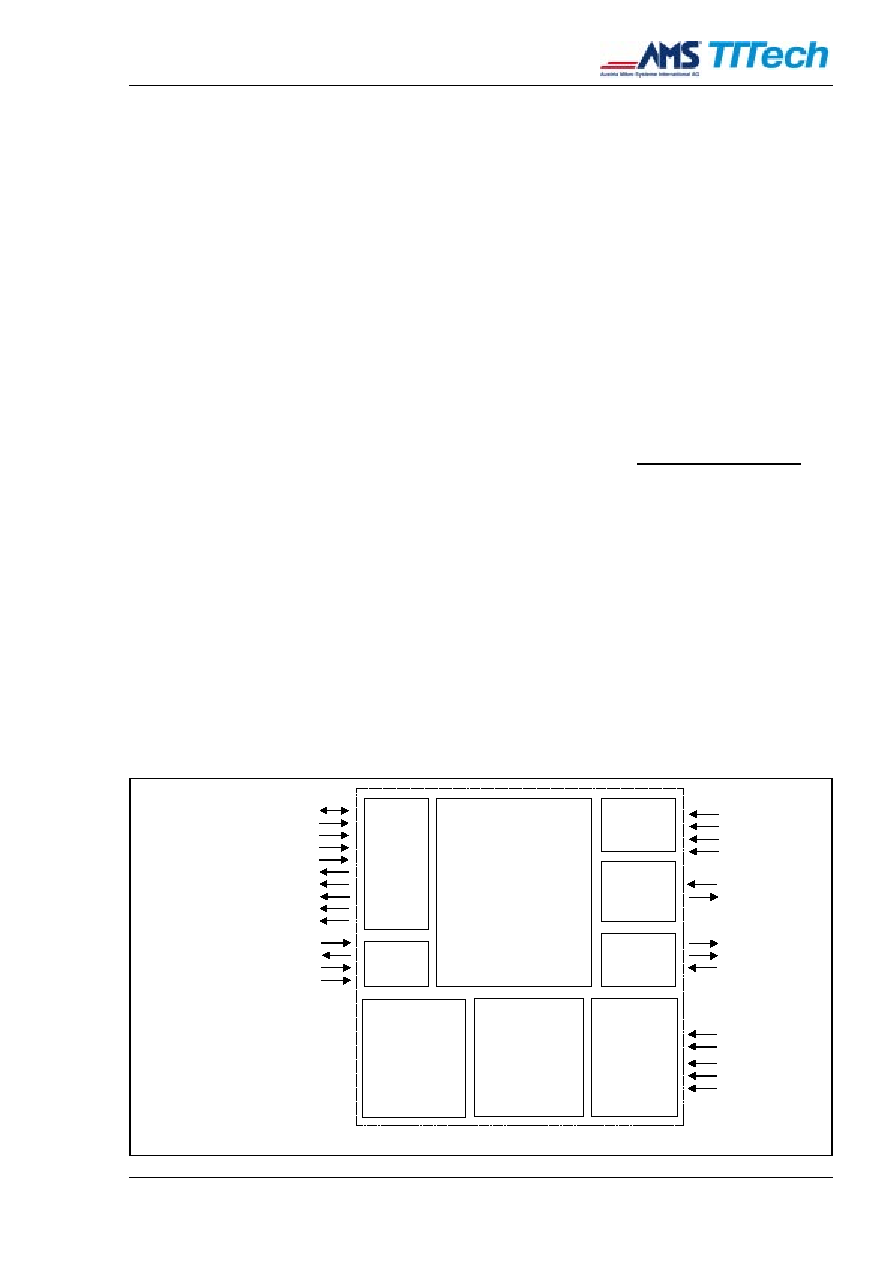
rxd[1:0]
rxclk[1:0]
rxdv[1:0]
rxer[1:0]
xin1
xout1
txd[1:0]
cts[1:0]
txclk[1:0]
test_se
ftest
stest
fidis
mtest
ram_data[15:0]
ram_address[11:0]
ram_ceb
ram_oeb
ram_web
ram_readyb
time_signalb
led[0]/time_tick
led[1]/time_overflow
led[2]/microtick
xin0
xout0
resetb
plloff
Quartz or
Oscillator
Controller
network
interface
(CNI)
TTP/C
protocol
processor core
Instruction
RAM memory
Network
configuration
memory
(MEDL)
TTP/C
Bus -
Media
Drivers
Bus
guardian
Receiver
Transmitter
Reset &
Time
base
Host
Processor
Interface
Test
Inter-
face
FLASH
memory
Figure 1 AS8202 Block Diagram

TTP/C-C2 Communication Controller ≠ Preliminary Data Sheet
AS8202
Rev. 1.0, October 2000
Page 3 of 3
The CNI (communication network interface) forms a temporal firewall. It decouples the
controller network from the host subsystem by use of a dual ported RAM. This prevents the
propagation of control errors. The interface to the host CPU is implemented as 16 bit wide non-
multiplexed asynchronous bus interface.
TTP/C follows a conflict-free media access strategy called time-division-multiple access
(TDMA). This means, TTP/C deploys a time slot technique based on a global time which is
permanently synchronised. Each node is assigned a time slot in which it is allowed to perform
transmit operation. The sequence of time slots is called TDMA round, a set of TDMA rounds
forms a cluster cycle. After one cluster cycle the operation of the network repeats. The
sequence of interactions forming the cluster cycle is defined in a static time schedule, called
message-descriptor-list (MEDL). The definition of the MEDL in conjunction with the global time
determines the response time for a service request.
The membership of all nodes in the network is evaluated by the communication controller. This
information is presented in a consistent fashion to all correct cluster members. During
operation, the status of every other node is propagated within one TDMA round. The MEDL is
loaded into the configuration memory when the system starts up.
P a c k a g e a n d P i n A s s i g n m e n t
Type: TQFP 80, plastic package
ram
-
a
ddr
es
s
[
3
]
test-se
AS8202
TTP/C
Communications
Controller
(TOP VIEW)
xo
u
t
0
Vd
d
xi
n0
txd
[
0
]
Vs
s
cts
[
0
]
rx
e
r
[
0
]
t
xcl
k
[
0
]
r
xcl
k
[
0
]
rx
d
[
0
]
rx
dv[
0
]
Vd
d
txd
[
1
]
Vs
s
cts
[
1
]
rx
e
r
[
1
]
t
xcl
k
[
1
]
r
xcl
k
[
1
]
rx
d
[
1
]
rx
dv
[
1
]
ram-d
a
t
a
[
7
]
ram-d
a
t
a
[
5
]
ram-d
a
t
a
[
6
]
ram-d
a
t
a
[
4
]
ram-d
a
t
a
[
2
]
ram-d
a
t
a
[
3
]
ram-d
a
t
a
[
1
]
ram-d
a
t
a
[
0
]
Vd
d
ram
-
a
ddr
es
s
[
10
]
ram
-
a
ddr
es
s
[
11
]
ram
-
a
ddr
es
s
[
9
]
ram
-
a
ddr
es
s
[
7
]
ram
-
a
ddr
es
s
[
8
]
ram
-
a
ddr
es
s
[
6
]
Vs
s
ram
-
a
ddr
es
s
[
5
]
ram
-
a
ddr
es
s
[
4
]
stest
resetb
ftest
fidis
plloff
led[2]/time-overflow
Vdd
Vss
time-signalb
led[0]/microtick
led[1]/time-tick
mtest
ram-address[0]
ram-address[1]
ram-address[2]
ram-ceb
Vss
Vdd
ram-data[15]
ram-data[14]
ram-data[13]
ram-data[12]
n.c.
n.c.
to Vdd
to Vss
ram-readyb
ram-web
ram-oeb
ram-data[11]
ram-data[10]
Vs
s
1
20
21
40
41
60
61
80
Vss
xin1
xout1
Vdd
ram-data[9]
ram-data[8]
Vss
Vdd
Figure 2 TQFP 80 pin package and pin assignment

TTP/C-C2 Communication Controller ≠ Preliminary Data Sheet
AS8202
Rev. 1.0, October 2000
Page 4 of 4
P i n D e s c r i p t i o n
Pin Name
Dir
Description
1,12,21,32,51,61,71
Vdd
P
positive power supply
4,13,24,33,43,52,62,72
Vss
P
Negative power supply
2
xout0
O
Main clock: analog pad from oscillator / leave open
when providing external clock
3
xin0
I
Main clock: analog pad from oscillator / use as input
when providing external clock
5
txd[0] O
PU
Transmit data channel 0
6
cts[0] O
PD
Transmit enable channel 0
7
txclk[0] I
PD
TTP/C synchronous: Transmit clock channel 0
8 rxer[0]
I
PU
TTP/C synchronous: Receive error channel 0
9
rxclk[0] I
PD
TTP/C synchronous: Receive clock channel 0
10 rxdv[0]
I
PU
TTP/C synchronous: Receive data valid channel 0
11
rxd[0] I
PU
Receive data channel 0
14
txd[1] O
PU
Transmit data channel 1
15
cts[1] O
PD
Transmit enable channel 1
16
txclk[1] I
PD
TTP/C synchronous: Transmit clock channel 1
17 rxer[1]
I
PU
TTP/C synchronous: Receive error channel 1
18
rxclk[1] I
PD
TTP/C synchronous: Receive clock channel 1
19 rxdv[1]
I
PU
TTP/C synchronous: Receive data valid channel 1
20
rxd[1] I
PU
Receive data channel 1
22
xout1
O
Bus guardian clock: analog pad from oscillator / leave
open when providing external clock
23
xin1
I
Bus guardian clock: analog pad from oscillator / use as
input when providing external clock
25 test_se
I
PD
Test input, connect to Vss
26 stest
I
PD
Test input, connect to Vss
27 plloff
I
PD
PLL
disable
pin
28
ftest I
PD
Test input, connect to Vss
29 fidis
I
PD
Test input, connect to Vss
30
resetb
I
main reset input signal, active low
31 time_signalb
O
PU
CNI control signal, CNI time signal
34 led[0]/microtick
O
PD
Configurable: either generic output port (f.e. to drive
LEDs) or timing signal TIME_TICK
35 led[1]/time_tick
O
PD
Configurable: either generic output port (f.e. to drive
LEDs) or timing signal TIME_OVERFLOW
36 led[2]/time_overflow
O
PD
Configurable: either generic output port (f.e. to drive
LEDs) or timing signal TIME_OVERFLOW
37 mtest
I
PD
Test input, connect to Vss
38-42,44-50
ram_address[0:11]
I
Host interface (CNI) address bus
53-60,63-70
ram_data[0:15]
I/O
Host interface (CNI) data bus, tristate
73 ram_ceb
I
PU
Host interface (CNI) chip enable, active low
74 ram_oeb
I
PU
Host interface (CNI) output enable, active low
75 ram_web
I
PU
Host interface (CNI) write enable, active low
76 ram_readyb
O
PU
Host interface (CNI) transfer finish signal, active low
77
to Vss
P
Connect to Vss
78
to Vdd
I
PU
Connect to Vdd
79
high Z
Do not connect
80
high Z
Do not connect
I
Input
CMOS
I
PU
Input CMOS with pull up
I
PD
Input CMOS with pull down
O
Output CMOS
O
PD
Output with pull down when tristate
O
PU
Output with pull up when tristate
I/O Input/Output CMOS tristate
P
Power Pin

TTP/C-C2 Communication Controller ≠ Preliminary Data Sheet
AS8202
Rev. 1.0, October 2000
Page 5 of 5
E l e c t r i c a l S p e c i f i c a t i o n s
Absolute Maximum Ratings (Non Operating)
SYMBOL PARAMETER
MIN
MAX
NOTE
VDD
DC Supply Voltage
-0.3 V
5.0 V
V
in
Input Voltage on any Pin
- 0.3 V
VDD + 0.3 V
I
in
Input Current on any Pin
-100 mA
100 mA
25∞C
T
strg
Storage
Temperature -55
oC 150
oC
T
sold
Soldering
Temperature
260
oC
1)
t
sold
Soldering Time
10 sec
Reflow and Wave
H
Humidity
5 %
85 %
ESD
Electrostatic Discharge
1000 V
HBM: R = 1.5 k , C = 100 pF
1. 300
oC all ceramic packages and DIL plastic packages, 260 oC for surface mounting plastic packages
Note: Stresses above those listed under "Absolute Maximum Ratings" may cause permanent damage to
the device. This is a stress rating only and functional operation of the device at these or any other
conditions above those indicated in the operational sections of this specification is not implied. Exposure
to absolute maximum rating conditions for extended periods may effect device reliability (e.g. hot carrier
degradation).
Recommended Operating Conditions
PARAMETER
SYMBOL MIN
TYP
MAX
NOTE
DC Supply Voltage
VDD
3.0 V
3.3 V
3.6 V
1)
Circuit Ground
VSS
0.0 V
0.0 V
0.0 V
Static Supply Current
IDDS
----
700
µ
A 800
µ
A
2)
Operating Supply Current
IDD
----
45 mA
56 mA
fCLK = 40 MHz, VDD = 3.6 V
3)
Main clock frequency
CLK
5 MHz
20 MHz
oscillator pins xin0, xout0
Bus Guardian clock
frequency
CLK2
4 MHz
16 MHz
oscillatpr pins xin1, xout1
Ambient Temperature
Ta
-40 oC
+125 oC
1)
1. The input and output parameter values in this table are directly related to ambient temperature and DC supply
voltage. A temperature range other Ta
min
to Ta
max
or a supply voltage range other than VDD
min
to VDD
max
will
affect these values and must be evaluated extra.
2. Static supply current IDDS is exclusive of input/output drive requirements and is measured at maximum VDD
with the clocks stopped and all inputs tied to VDD or VSS, configured to draw minimum current.
3. Operating current is exclusive of input/output drive requirements and is measured at maximum VDD and
maximum clock frequency 40 MHz.
DC Characteristics and Voltage Levels
CMOS I/O levels for specified voltage and temperature range unless otherwise noted.
Inputs Pins
Pin Name
Vil
Vih
Iil (1)
Iih(2)
NOTE
max
min
min
max
min
max
All inputs and IO pins
without pull-up/down
30%
VDD
70%
VDD
NA -1.0
µ
A
NA 1.0
µ
A
CMOS input (3)
Inputs with pull-up
30%
VDD
70%
VDD
-50
µ
A
-160
µ
A
NA
NA
CMOS with
pull up (3)
Inputs with pull-down
30%
VDD
70%
VDD
NA NA
30
µ
A
160
µ
A
CMOS with
pull down (3)
1. Iil ist tested at VDDmax and Vin = 0
2. Iih ist tested at VDDmax and Vin = VDDmax
3. CMOS input levels are in percentage of VDD, for pull-up/down refer to pin description above.

TTP/C-C2 Communication Controller ≠ Preliminary Data Sheet
AS8202
Rev. 1.0, October 2000
Page 6 of 6
Output Pins
Pin Name
Vol
Voh
Iol (1)
Ioh(2)
Ioz(3)
NOTE
V
V
mA
mA
µ
A
txd[0,1],cts[0,1],led[0,2]
0.4
2.4
4.0
-4.0
NA
CMOS output
All other output pins
(except xout0, xout1)
0.4
2.4
2.0
-2.0
NA
CMOS output
All I/O pins
0.4
2.4
2.0
-2.0
+/-10
CMOS output, Tristate
1. Vol, Iol is tested at VDD = 3.3V
2. Voh, Ioh is tested at VDD = 3.3V
3. Ioz is tested at VDD = 3.6V
AC Characteristics
PARAMETER
SYMBOL
PIN
MIN
MAX
NOTE
main clock external operating
frequency
clkext
xin0
0
40 MHz
pin plloff = high
PLL not used
main clock XTAL0 frequency
clkxt0
xin0/xout0
1 MHz
20 MHz
oscillator cell 1
1)
main internal clock frequency
clk0
---
---
40 MHz
pin plloff = low PLL
in use
1)
XTAL1 operating frequency
clkxt1
xin1/xout1
1 MHz
20 MHz
oscillator cell 2
1)
1. XTAL frequency or external clock frequency for PLL input is fixed to 10 MHz, other frequencies applicable only
without PLL function in use.
TTP/C-C2 Communication Controller ≠ Preliminary Data Sheet
AS8202
Rev. 1.0, October 2000
Page 7 of 7
A p p l i c a t i o n I n f o r m a t i o n
Host CPU Interface
The host CPU interface also referred as CNI (communication network interface) connects the
application circuitry to the TTP controller. All ram_-lines provide asynchronous read/write
access to a dual ported RAM. There are no setup/hold constraints referred to the microtick
(main clock "clk0"). The signals have to be applied for certain duration to be synchronized to
the main internal clock (microtick). The time_-lines signal to host CPU the global synchronous
time of the TTP network and determine when to deliver, resp. to fetch data from the host
interface. One of the lines may be connected to an interrupt input of the host CPU. Note that
the microtick, time_overflow and the time_tick pins can be configured as general purpose
output LED pins (see the LED Interface section below).
Host Interface Ports
Pin Name
mode
width
comment
ram_address[0:11]
in
12
DPRAM address bus, 12 bit
ram_data[0:15]
inout (tri)
16
DPRAM data bus, 16 bit
ram_ceb
In
1
DPRAM chip enable
ram_web
In
1
DPRAM write enable
ram_oeb
In
1
DPRAM output enable
ram_readyb out
1
DPRAM
ready
time_overflow
out
1
Overflow of global time (global time is Zero)
microtick
out
1
Microtick (internal main clock)
time_signal
out
1
CNI time signal
time_tick
out
1
Macrotick (global time is incremented)
Asynchronous DPRAM interface
Signals ram_address[0:11] and ram_web have to be stable before the falling edge of ram_ceb
For a write access the host sets ceb, web, address and data until the DPRAM has taken the
data and set readyb active low. The next access may start with readyb inactive again. A read
cycle starts with valid address and ceb, the data is valid with readyb active low. A low level on
oeb and ceb switches the data bus from tristate to output. Access times depend on the
controller clock rate and controller activity, typical values are:
controller cycle time
Tc
Min 25 ns (40 MHz)
write time
Tw
Min 4 Tc
read time
Tr
Min 5 Tc
readyb low time
Trb
Min 1 Tc
Trb
Trb
xx
tristate
valid
valid
ceb
addres
data
web
oeb
ready
b
valid
valid
write
read
Tw
Tr

TTP/C-C2 Communication Controller ≠ Preliminary Data Sheet
AS8202
Rev. 1.0, October 2000
Page 8 of 8
Reset and Oscillator
Pin Name
mode
width
Comment
xin0
in
1
main oscillator input
xout0
out
1
main oscillator output
xin1
in
1
bus guardian oscillator input
xout1
out
1
bus guardian oscillator output
plloff
in 1 PLL
disable
resetb
in
1
external reset
Table 1: Reset and Oscillator Ports
External Reset Signal
To issue a reset of the chip the resetb port has to be driven low for at least
µ
s. After
power-up the reset must overlap the build-up time of the oscillator circuit.
Integrated Power-On Reset
The Device has an internal Power-On Reset generator. When supply voltage ramps up, the
internal reset signal is kept active (low) for about 33 µs typical.
Parameter
Symbol
Min
Typ
Max
Unit
supply voltage slope
dV/dt
250
-
-
kV/s
power on reset active time after VDD > 1,0V
t
pon_res
25
33 49
us
Oscillator circuitry
The internal oscillator cell requires an external quartz or an external oscillator respectively. The
frequency applied on the main clock input (xin0, xout0) can be reduced by a factor of four by
using the internal PLL. In order to generate an internal frequency of 40 MHz using the internal
PLL, an external quartz or quartz oscillator with a frequency of 10 MHz is connected and the
plloff input is tied low. The bus guardian clock has no internal PLL.
Figure 3: Quartz Circuit PLL off
Figure 4: Quartz Circuit PLL on
Figure 5: Oscillator Circuit
xin0
xout1 xin1
10MHz
16MHz
AS8202
p
llo
ff
,0`
xout0
40 MHz
xin0
xout1 xin1
20MHz
16MHz
AS8202
p
llo
ff
,1`
xout0
20 MHz
xin0
xout1 xin1
40MHz
oscillator
16MHz
oscillator
AS8202
p
llo
ff
,1`
xout0
40 MHz
n.c.
n.c.
TTP/C-C2 Communication Controller ≠ Preliminary Data Sheet
AS8202
Rev. 1.0, October 2000
Page 9 of 9
TTP/C Asynchronous Bus Interface
The TTP/C asynchronous bus interface uses MFM patterns to transmit/receive signals at a
maximum data rate of 5 MBit/s on a shared media (physical bus). The pins can either be
connected to drivers using recessive/dominant states on the wire as well as drivers using active
push/pull functionality.
Pin Name
mode
comment
txd[0]
out
Transmit data channel 0
cts[0]
out
Transmit enable channel 0
txclk[0]
in
no function (do not connect)
rxer[0]
in
no function (do not connect)
rxclk[0]
in
no function (do not connect)
rxdv[0]
in
no function (do not connect)
rxd[0]
in
Receive data channel 0
txd[1]
out
Transmit data channel 1
cts[1]
out
Transmit enable channel 1
txclk[1]
in
no function (do not connect)
rxer[1]
in
no function (do not connect)
rxclk[1]
in
no function (do not connect)
rxdv[1]
in
no function (do not connect)
rxd[1]
in
Receive data channel 1
Table 2: TTP/C Asynchronous Bus Interface Pins
TTP/C Synchronous Bus Interface
The TTP/C synchronous bus interface uses a synchronous transfer method to transfer data at
a rate of 25 MBit/s. PHY drivers used in commercial 100 MBit Ethernet applications can be
connected to this interface.
Pin Name
mode
comment
txd[0]
out
Transmit data channel 0
cts[0]
out
Transmit enable channel 0
txclk[0]
in
Transmit clock channel 0
rxer[0]
in
Receive error channel 0
rxclk[0]
in
Receive clock channel 0
rxdv[0]
in
Receive data valid channel 0
rxd[0]
in
Receive data channel 0
txd[1]
out
Transmit data channel 1
cts[1]
out
Transmit enable channel 1
txclk[1]
in
Transmit clock channel 1
rxer[1]
in
Receive error channel 1
rxclk[1]
in
Receive clock channel 1
rxdv[1]
in
Receive data valid channel 1
rxd[1]
in
Receive data channel 1
Table 3: TTP/C Synchronous Bus Interface Pins

TTP/C-C2 Communication Controller ≠ Preliminary Data Sheet
AS8202
Rev. 1.0, October 2000
Page 10 of 10
Test Interface
The Test Interface supports the manufacturing test and characterisation of the chip. In the
application environment test pins and special pins have to be connected as following:
test_se, stest, ftest, fidis, mtest, Vpp : connect to Vss
Tmr : connect to Vdd
Tm0, Tm1 : do not connect
Warning:
Any other connection of this pins may cause permanent damage to the device.
LED Signals
The LED signals can be used as a universal output port. The driver strength of the LED ports is
4mA. Note that the pins can be configured as special-function host interface pins (see the Host
Interface section for more details).
O r d e r i n g I n f o r m a t i o n
Part Number:
AS8202
Part Name:
TTP/C-C2 Communication Controller
Package: TQFP
80
S u p p o r t
Software tools, hardware development boards, evaluation systems and extensive support on
TTP system integration as well as consulting is provided by:
TTTech Computertechnik AG
Time-Triggered Technology
and
TTChip GmbH ≠ a TTTech Company
Schoenbrunnerstrasse 7
A1040 Vienna
Austria
Voice: +43 1 5853434 - 0
Fax:
+43 1 5853434 - 90
email: office@tttech.com
web: http://www.tttech.com
Note: TTP
Æ
is a registered trademark of FTS Computertechnik GmbH. All other trademarks are the property oftheir respective
holders.
Copyright
©
2000 TTTech Computertechnik AG
Copyright
©
2000, Austria Mikro Systeme International AG, Schloþ Premst‰tten, 8141 Unterpremst‰tten, Austria.
Telefon +43-(0)3136-500-0, Telefax +43-(0)3136-52501, E-Mail info@amsint.com
All rights reserved. No part of this publication may be reproduced, stored in a retrieval system, or transmitted, in any form or by any
means, without the prior permission in writing by the copyright holder. To the best of its knowledge, Austria Mikro Systeme
International asserts that the information contained in this publication is accurate and correct.