 | –≠–ª–µ–∫—Ç—Ä–æ–Ω–Ω—ã–π –∫–æ–º–ø–æ–Ω–µ–Ω—Ç: AS8205 | –°–∫–∞—á–∞—Ç—å:  PDF PDF  ZIP ZIP |

AS8205
TTP/C-C2XNF StarCoupler
Central BusGuardian
Preliminary Data Sheet
Rev. 1.0, September 2002

AS8205
TTP/C-C2XNF StarCoupler ≠ Preliminary Data Sheet
Rev. 1.0, September 2002
uncontrolled copy
Page 2
of
20
1 R e vi s i o n
Date Nr
Modification
Name Department
27.09.2002
1 New edition
W. Ettlmayr
TTChip/Design

AS8205
TTP/C-C2XNF StarCoupler ≠ Preliminary Data Sheet
Rev. 1.0, September 2002
uncontrolled copy
Page 3
of
20
2 C o n t e n ts
1
Revision
2
2
Contents
3
3
Key Features
4
4
General Description
4
5
Package and Pin Assignment
6
6
Pin Description
7
7
Electrical Specifications
10
7.1
A
BSOLUTE
M
AXIMUM
R
ATINGS
(N
ON
O
PERATING
) 10
7.2
R
ECOMMENDED
O
PERATING
C
ONDITIONS
10
7.3
DC
C
HARACTERISTICS AND
V
OLTAGE
L
EVELS
11
7.3.1
I
NPUTS
P
INS
11
7.3.2
O
UTPUT
P
INS
11
8
Application Information
12
8.1
H
OST
CPU
I
NTERFACE
12
8.2
R
ESET AND
O
SCILLATOR
14
8.2.1
E
XTERNAL
R
ESET
S
IGNAL
14
8.2.2
I
NTEGRATED
P
OWER
-O
N
R
ESET
14
8.2.3
O
SCILLATOR CIRCUITRY
14
8.3
TTP/C
A
SYNCHRONOUS
B
US
I
NTERFACE
15
8.4
T
EST
I
NTERFACE
16
8.5
LED
S
IGNALS
16
9
Mechanical Information
17
10
Ordering Information
20
11
Support
20

AS8205
TTP/C-C2XNF StarCoupler ≠ Preliminary Data Sheet
Rev. 1.0, September 2002
uncontrolled copy
Page 4
of
20
3 K e y F e a t u r e s
∑ Dedicated busguardian supporting TTP/C (time triggered protocol class C)
∑ Suited for dependable distributed real-time systems with guaranteed response time
∑ Application fields: Automotive (by-wire braking, steering, vehicle dynamics control, drive
train control), Aerospace (aircraft electronic systems), Industrial systems, Railway systems
∑ TTP/C asynchronous data rate up to 5 MBit/s @ clock 40 MHz
∑ Single power supply 3.3V
∑ 0.35µm CMOS process
∑ Temperature range: -40∞C to 125∞ C
∑ 16 Ports for serial communication with TTP/C nodes
∑ per port configurable encoding: MFM/Manchester
∑ Signal reshaping to avoid byzantine scenarios
∑ 2k x 16 SRAM for message, status and control area (communication network interface)
∑ 8k x 16 SRAM for MEDL configuration data (MEDL can be decreased in steps of 2k x 16 to
get more CNI RAM)
∑ 4k x 16 SRAM for instruction code and configuration data
∑ 4k x 16 Boot ROM
∑ 16 Bit non-multiplexed host CPU interface
∑ 16 Bit RISC architecture
∑ software tools, design-in support, development boards available (
http://www.tttech.com/
)
∑
120 pin LQFP Package, body size 14 x 14mm, 0.4mm pitch
4 G e n e r a l D e s c r i p t i o n
The AS8205 starcoupler is an integrated device supporting serial communication according to
the TTP/C specification. It performs all communication tasks such as reception and transmis-
sion of messages in a TTP
cluster without interaction of a host CPU.
TTP
provides mechanisms that allow the deployment of high-dependability distributed real-
time systems. It provides following services:
∑ predictable transmission of messages with minimal jitter
∑ fault-tolerant distributed clock synchronisation
∑ consistent membership service with small delay
∑ masking of single faults
The Task of the Central Busguardian as an independent unit is to isolate faulty nodes (e.g.
babbling idiots) from the cluster. The Central Busguardian provides writeaccess to the shared
medium to every node according to the timing information stored in the SWIDL (Switch descrip-
tor list). This ensures that each connected node only sends in its own timeslot. The SWIDL is
generated from the TTTech-toolchain like the MEDL during clusterdesign. The Central Bus-
guardian has an integrated TTP/C controller (C2NF) to perform tasks like global time synchro-
nisation, membership calculation, integration during systemstartup, integration into a running
cluster, etc. Another task of the Central Busguardian is to make sure that every connected
node gets the same information to avoid byzantine scenarios. Therefore it decodes the incom-
ing signal and encodes it again (reshape-unit). This reshaped signal is then provided to all other
nodes.

AS8205
TTP/C-C2XNF StarCoupler ≠ Preliminary Data Sheet
Rev. 1.0, September 2002
uncontrolled copy
Page 5
of
20
C-state
Central Bus
Guardian
Bus Access
Controler
Reshape Unit
Mode[1:0],
ParamBus[m:0]
Enable[p:0][1:0]
DigitalData[n:0]
ActivitySense[k:0]
ChannelNo
St
ar
t
W
in
do
w
Lin
k
[
n
]
RX
TX
Enable[1:0]
Stub Bus
Guardian
SharedChannel RX
Stub Bus
Guardian
Stub Bus
Guardian
Enable[1:0]
Enable[1:0]
SharedChannel RX
Lin
k
[
0
]
RX
TX
Lin
k
[
1
]
RX
TX
SharedChannel RX
Channel
Multiplexer
Dedicated Interface
Interlink
TX
RX
Media
MUX
Shared
Channel
RX
SharedChannel TX MFM
SharedChannel TX MFM
SharedChannel TX
SharedChannel TX MFM
Interrupt
Line
TTP/C
Controller
RX1
RX0
Controller
part
MEDL/SWIDL
SWIDL information
Host Interface
CNI Ram
Host
Interface
Multiplexer
Data
Addr.
Da
ta
Addr
.
External
(optional)
Host CPU
SharedChannel TX Manchester
SharedChannel TX Manchester
SharedChannel TX Manchester
SharedChannel TX Manchester
Manchester
MFM
Figure 1: AS8205 Block Diagram

AS8205
TTP/C-C2XNF StarCoupler ≠ Preliminary Data Sheet
Rev. 1.0, September 2002
uncontrolled copy
Page 6
of
20
5 P a c k a g e a n d P i n As s i g n m e n t
GND
Power supply
AS8205
TTP/C-C2XNF
Communication Controller
(Star Coupler)
TOP VIEW
76
75
74
73
72
71
70
69
68
67
66
65
64
63
62
61
60
59
58
57
56
55
54
53
52
51
50
49
48
47
46
45
80
79
78
77
44
43
42
41
116
115
114
113
112
111
110
109
108
107
106
105
104
103
102
101
100
99
98
97
96
95
94
93
92
91
90
89
88
87
86
85
120
119
118
117
84
83
82
81
5
6
7
8
9
11
12
13
14
15
16
17
18
19
20
21
22
23
24
25
26
27
28
29
30
31
32
33
34
35
36
1
2
3
4
37
38
39
40
VDD
GND
RX
D
0
6
TX
D
0
6
CT
S
0
6
RXD03
TXD03
CTS03
RXD04
TXD04
CTS04
RXD05
TXD05
CTS05
RX
D
0
7
TX
D
0
7
CT
S
0
7
RX
D
0
8
TX
D
0
8
CT
S
0
8
RXD0
9
TX
D
0
9
CT
S
0
9
RXD1
0
TX
D
1
0
CT
S
1
0
RX
D
1
1
TX
D
1
1
CT
S
1
1
RXD1
2
TX
D
1
2
CT
S
1
2
RXD1
3
TX
D
1
3
CT
S
1
3
RXD1
4
TX
D
1
4
CTS14
RXD15
TXD15
CTS15
RXD16
TXD16
CTS16
RXD02
TXD02
CTS02
RXD01
TXD01
CTS01
VDD
GN
D
D0
D1
D2
D3
D4
D5
D6
D7
D15
D8
D9
D10
D11
D12
D13
D14
A1
A0
A2
A3
A4
A1
1
A1
0
A9
A8
A7
A6
A5
LED2
LED1
LED0
RE
S
E
T
B
TR
S
T
INTB
XTALI
XTALO
GND
GND
VDD
TD
I
TD
O
TM
S
TC
K
10
SC_TX
SC_RX
Symbols:
Oscillator
VDD
GND
VDD
GND
VD
D
GN
D
TM
R
CE
B
OE
B
WE
B
RE
AD
Y
B
MT
ES
T
ST
E
S
T
T
EST
-
S
E
FT
E
S
T
FI
D
I
S
PLLOFF
SC_CTS
LED3
LED4
LED5
BusGuardian Pins
C2NF Pins
JTAG Pins
VD
D
GND
Figure 2: LQFP 120 pin package and pin assignment
For mechanical dimensions see chapter 9 Mechanical Information.

AS8205
TTP/C-C2XNF StarCoupler ≠ Preliminary Data Sheet
Rev. 1.0, September 2002
uncontrolled copy
Page 7
of
20
6 P i n D e s c r i p t i o n
Pin Name
Dir Description
1 RXD06
IPU
Receive Data Link 06
2 TXD06
OPU
Transmit Data Link 06
3 CTS06
OPD
Clear To Send Link 06
4 RXD07
IPU
Receive Data Link 07
5 TXD07
OPU
Transmit Data Link 07
6 CTS07
OPD
Clear To Send Link 07
7 RXD08
IPU
Receive Data Link 08
8 TXD08
OPU
Transmit Data Link 08
9 VDD
P
positive power supply
10 VSS
P
negative power supply
11 CTS08
OPD
Clear To Send Link 08
12 RXD09
IPU
Receive Data Link 09
13 TXD09
OPU
Transmit Data Link 09
14 CTS09
OPD
Clear To Send Link 09
15 RXD10
IPU
Receive Data Link 10
16 TXD10
OPU
Transmit Data Link 10
17 CTS10
OPD
Clear To Send Link 10
18 RXD11
IPU
Receive Data Link 11
19 TXD11
OPU
Transmit Data Link 11
20 CTS11
OPD
Clear To Send Link 11
21 VDD
P
positive power supply
22 VSS
P
negative power supply
23 RXD12
IPU
Receive Data Link 12
24 TXD12
OPU
Transmit Data Link 12
25 CTS12
OPD
Clear To Send Link 12
26 RXD13
IPU
Receive Data Link 13
27 TXD13
OPU
Transmit Data Link 13
28 CTS13
OPD
Clear To Send Link 13
29 RXD14
IPU
Receive Data Link 14
30 TXD14
OPU
Transmit Data Link 14
31 CTS14
OPD
Clear To Send Link 14
32 RXD15
IPU
Receive Data Link 15
33 TXD15
OPU
Transmit Data Link 15
34 CTS15
OPD
Clear To Send Link 15
35 RXD16
IPU
Receive Data Link 16
36 TXD16
OPU
Transmit Data Link 16
37 CTS16
OPD
Clear To Send Link 16
38 SC_RX
IPU
Receive Data InterLink
39 VDD
P
positive power supply
40 VSS
P
negative power supply
41 SC_TX
OPU
Transmit Data InterLink
42 SC_CTS
OPD
Clear To Send InterLink
43 D0
I/O
Host interface (CNI) data bus, tristate
44 D1
I/O
Host interface (CNI) data bus, tristate
45 D2
I/O
Host interface (CNI) data bus, tristate
46 D3
I/O
Host interface (CNI) data bus, tristate
47 D4
I/O
Host interface (CNI) data bus, tristate

AS8205
TTP/C-C2XNF StarCoupler ≠ Preliminary Data Sheet
Rev. 1.0, September 2002
uncontrolled copy
Page 8
of
20
48 D5
I/O
Host interface (CNI) data bus, tristate
49 D6
I/O
Host interface (CNI) data bus, tristate
50 D7
I/O
Host interface (CNI) data bus, tristate
51 VDD
P
positive power supply
52 LED5
OPD
generic output port (f.e. to drive LEDs)
52 VSS
P
negative power supply
53 D8
I/O
Host interface (CNI) data bus, tristate
53 LED4
OPD
generic output port (f.e. to drive LEDs)
54 D9
I/O
Host interface (CNI) data bus, tristate
54 LED3
OPD
generic output port (f.e. to drive LEDs)
55 D10
I/O
Host interface (CNI) data bus, tristate
56 D11
I/O
Host interface (CNI) data bus, tristate
57 D12
I/O
Host interface (CNI) data bus, tristate
58 D13
I/O
Host interface (CNI) data bus, tristate
59 D14
I/O
Host interface (CNI) data bus, tristate
60 D15
I/O
Host interface (CNI) data bus, tristate
61 A0
I
Host interface (CNI) address bus
62 A1
I
Host interface (CNI) address bus
63 A2
I
Host interface (CNI) address bus
64 A3
I
Host interface (CNI) address bus
65 A4
I
Host interface (CNI) address bus
66 A5
I
Host interface (CNI) address bus
67 A6
I
Host interface (CNI) address bus
68 A7
I
Host interface (CNI) address bus
69 A8
I
Host interface (CNI) address bus
70 A9
I
Host interface (CNI) address bus
71 A10
I
Host interface (CNI) address bus
72 A11
I
Host interface (CNI) address bus
73 CEB
IPU
Host interface (CNI) chip enable, active low
74 OEB
IPU
Host interface (CNI) output enable, active low
75 VDD
P
positive power supply
76 VSS
P
negative power supply
77 WEB
IPU
Host interface (CNI) write enable, active low
78 READYB
OPU
Host interface (CNI) transfer finish signal, active low
79 TRST
IPU
JTAG: Reset
80 TDI
I
JTAG: Data in
81 TDO
O
JTAG: Data out
82 TCK
IPD
JTAG: Clock
83 TMS
IPD
JTAG: Mode select
84 FIDIS
IPD
Test input, connect to Vss
85 FTEST
IPD
Test input, connect to Vss
86 MTEST
IPD
Test input, connect to Vss
87 TEST_SE
IPD
Test input, connect to Vss
88 STEST
IPD
Test input, connect to Vss
89 TMR
IPU
Connect to Vdd
90 RESETB
I
Main reset input signal, active low
91 PLLOFF
IPD
PLL disable pin
95 LED2/TIME_OVERFLOW
OPD
Configurable: either generic output port (f.e. to drive
LEDs) or timing signal TIME_OVERFLOW
96 LED1/TIME_TICK
OPD
Configurable: either generic output port (f.e. to drive
LEDs) or timing signal TIME_OVERFLOW

AS8205
TTP/C-C2XNF StarCoupler ≠ Preliminary Data Sheet
Rev. 1.0, September 2002
uncontrolled copy
Page 9
of
20
97 LED0/MICROTICK
OPD
Configurable: either generic output port (f.e. to drive
LEDs) or timing signal TIME_TICK
98 INTB
OPU
CNI control signal, CNI time signal
99 VDD
P
positive power supply
100 VSS
P
negative power supply
101 XOUT0
O
Main clock: analog pad from oscillator / leave open
when providing external clock
102 XIN0
I
Main clock: analog pad from oscillator / use as input
when providing external clock
103 VSS
P
negative power supply
104 RXD01
IPU
Receive Data Link 01
105 TXD01
OPU
Transmit Data Link 01
106 CTS01
OPD
Clear To Send Link 01
107 RXD02
IPU
Receive Data Link 02
108 TXD02
OPU
Transmit Data Link 02
109 CTS02
OPD
Clear To Send Link 02
110 RXD03
IPU
Receive Data Link 03
111 VDD
P
positive power supply
112 VSS
P
negative power supply
113 TXD03
OPU
Transmit Data Link 03
114 CTS03
OPD
Clear To Send Link 03
115 RXD04
IPU
Receive Data Link 04
116 TXD04
OPU
Transmit Data Link 04
117 CTS04
OPD
Clear To Send Link 04
118 RXD05
IPU
Receive Data Link 05
119 TXD05
OPU
Transmit Data Link 05
120 CTS05
OPD
Clear To Send Link 05
Table 1: Pin description

AS8205
TTP/C-C2XNF StarCoupler ≠ Preliminary Data Sheet
Rev. 1.0, September 2002
uncontrolled copy
Page 10
of
20
7 E l e c t r i c a l S p e c i f i c a t i o n s
7.1 Absolute Maximum Ratings (Non Operating)
SYMBOL PARAMETER
MIN
MAX
NOTE
VDD
DC Supply Voltage
-0.3 V
5.0 V
V
in
Input Voltage on any Pin
- 0.3 V
VDD + 0.3 V
I
in
Input Current on any Pin
-100 mA
100 mA
25∞C
T
strg
Storage
Temperature -55 oC 150
oC
T
sold
Soldering
Temperature
260 oC
1
t
sold
Soldering Time
10 sec
Reflow and Wave
H
Humidity
5 %
85 %
ESD
Electrostatic Discharge
1000 V
HBM: R = 1.5 k
, C = 100 pF
Table 2: Absolute maximum ratings
1. 300
oC all ceramic packages and DIL plastic packages, 260 oC for surface mounting plastic packages
Note: Stresses above those listed under "Absolute Maximum Ratings" may cause permanent damage to
the device. This is a stress rating only and functional operation of the device at these or any other condi-
tions above those indicated in the operational sections of this specification is not implied. Exposure to
absolute maximum rating conditions for extended periods may affect device reliability (e.g. hot carrier
degradation).
7.2 Recommended Operating Conditions
PARAMETER SYMBOL
MIN
TYP
MAX
DC Supply Voltage
1
VDD
3.0 V
3.3 V
3.6 V
Circuit Ground
VSS
0.0 V
0.0 V
0.0 V
Ambient Temperature
1
Ta
-40 ∞C
+125 ∞C
Static Supply Current
2
IDDS
700
µ
A
800
µ
A
Operating Supply Current
3,4
IDD
45 mA
56 mA
clock period of main clock (external) using internal PLL
3,5
CLK0_ext_PLL
100
ns
clock period of main clock (external) without PLL
3
CLK0_ext
25
ns
Table 3: Recommended operating conditions
1. The input and output parameter values in this table are directly related to ambient temperature and DC supply
voltage. A temperature range other Ta
min
to Ta
max
or a supply voltage range other than VDD
min
to VDD
max
will af-
fect these values and must be evaluated extra.
2. Static supply current IDDS is exclusive of input/output drive requirements and is measured at VDD=max with the
clocks stopped and all inputs tied to VDD or VSS, configured to draw minimum current.
3. typical values: CLK0=40 MHz
4. Operating current is exclusive of input/output drive requirements and is measured at VDD=max.
5. Using the internal PLL multiples the main clock frequency by 4.

AS8205
TTP/C-C2XNF StarCoupler ≠ Preliminary Data Sheet
Rev. 1.0, September 2002
uncontrolled copy
Page 11
of
20
7.3 DC Characteristics and Voltage Levels
CMOS I/O levels for specified voltage and temperature range unless otherwise noted.
7.3.1 Inputs
Pins
Pin
Vil
Vih
Iil
1
Iih
2
MAX
MIN
MIN
µ
A
MAX
µ
A
MIN
µ
A
MAX
µ
A
All CMOS inputs and IO pins
without pull-up/down
3
30% VDD
70% VDD
NA
-1.0
NA
1.0
CMOS inputs with pull-up
4
30% VDD
70% VDD
-50.0
-160.0
NA
NA
CMOS inputs with pull-down
5
30% VDD
70% VDD
NA
NA
30.0
160.0
Analog inputs
6
20% VDD
80% VDD
NA
7
NA
7
NA
7
NA
7
Table 4: input pins
1. Iil is tested at VDD=max and Vin = VSS
2. Iih is tested at VDD=max and Vin = VDDmax
3. refers to the following pin classes: I, I/O (see pin descriptions)
4. refers to the following pin classes: I
PU
, O
PU
when output disabled (see pin descriptions)
5. refers to the following pin classes: I
PD
, O
PD
when output disabled (see pin descriptions)
6. refers to the following pins: XOUT0, XOUT1
7. To be defined
7.3.2 Output
Pins
Pin Name
Vol
Voh
Iol
1
Ioh
2
Ioz
3
MAX
V
MIN
V
MAX
mA
MIN
mA
MAX
µ
A
TXD[0,1], CTS[0,1], LED[2:0]
0.4
2.4
4.0
-4.0
NA
All other output pins
4
0.4 2.4 2.0 -2.0 NA
All I/O pins
0.4
2.4
2.0
-2.0
+/-10
XOUT0, XOUT1
5
NA NA NA NA NA
Table 5: output pins
1. Vol, Iol is tested at VDD = typ
2. Voh, Ioh is tested at VDD = typ
3. Ioz is tested at VDD = max
4. refers to the following pin classes: O
PU
and O
PD
when output enabled (see pin descriptions)
5. Pin output characteristics are only tested to verify quartz oscillation startup within limits
AS8205
TTP/C-C2XNF StarCoupler ≠ Preliminary Data Sheet
Rev. 1.0, September 2002
uncontrolled copy
Page 12
of
20
8 Ap p l i c a t i o n I n f o r m a t i o n
8.1 Host CPU Interface
The host CPU interface, also referred as CNI (communication network interface), connects the
application circuitry to the AS8205 TTP/C-controller. All related signal pins provide an asyn-
chronous read/write access to a dual ported RAM located in the AS8205. There are no
setup/hold constraints referred to the microtick (main clock "CLK0") but the signals have to be
applied for certain duration to be synchronized to the internal main clock.
The host interface features an interrupt or time signal INTB to notify the application circuitry of
programmed and protocol-specific, synchronous and asynchronous events.
READYB and INTB are open-drain outputs, i.e. the output is only driven to '0' and is weak-pull-
up at any other time, so external pull-up resistors or transistors may be necessary depending
on the application.
The LED port is software-configurable to automatically show some protocol-related states and
events, see below for the LED port configuration.
Host Interface Ports
Pin Name
mode
width
comment
A[11:0]
in
12
CNI address bus, 12 bit (A0 is LSB)
D[15:0]
inout (tri)
16
CNI data bus, 16 bit (D0 is LSB)
CEB
In
1
CNI chip enable, active low
WEB
In
1
CNI write enable, active low
OEB
In
1
CNI output enable, active low
READYB
out (open drain)
1
CNI ready, active low
INTB
out (open drain)
1
CNI interrupt, time signal, active low
Table 6: Host-Interface Ports

AS8205
TTP/C-C2XNF StarCoupler ≠ Preliminary Data Sheet
Rev. 1.0, September 2002
uncontrolled copy
Page 13
of
20
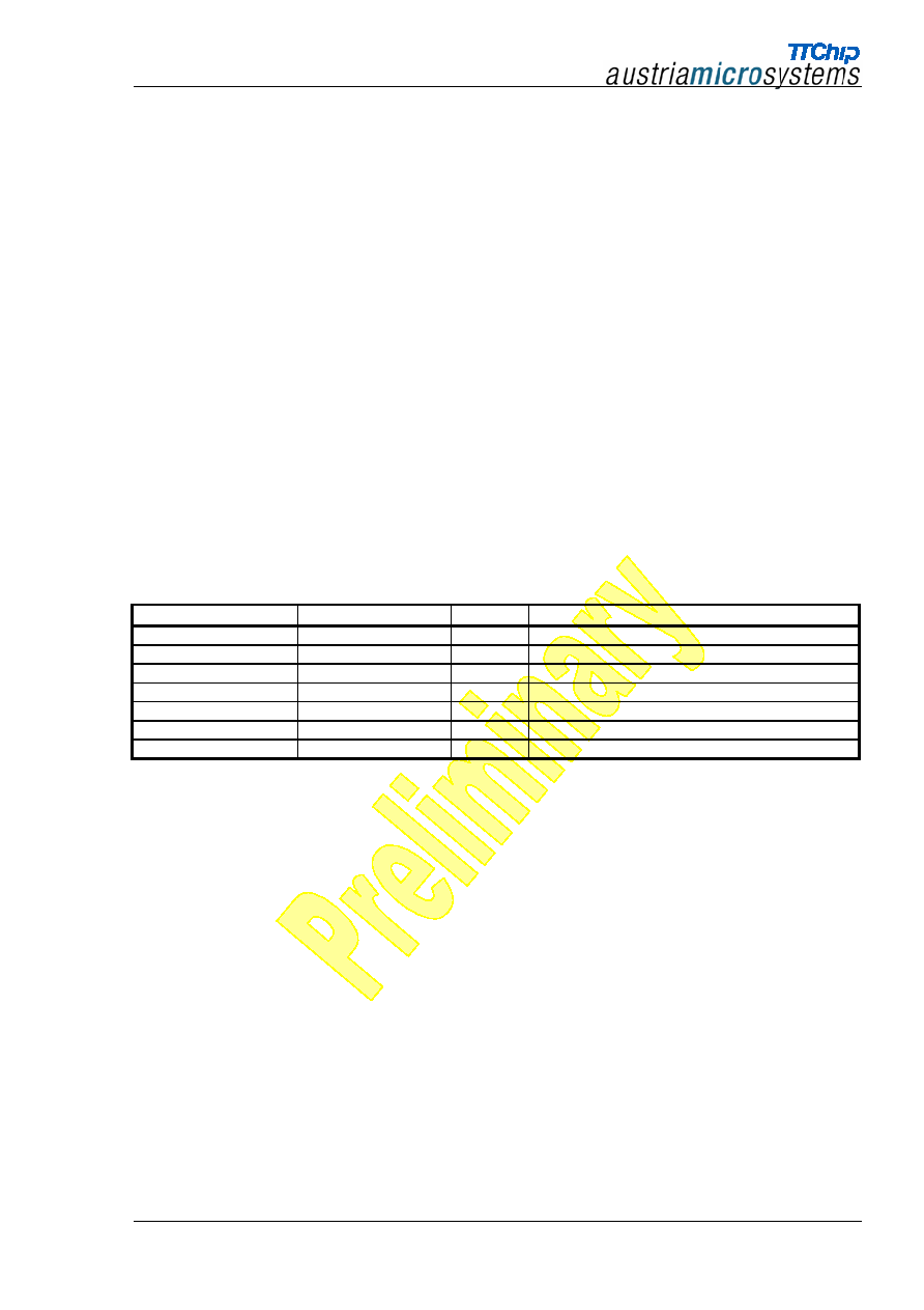
Asynchronous DPRAM interface
Characteristic
min
max
Tc
Controller cycle time
25 ns (40 MHz)
1a
Input Valid to CEB
(Setup Time)
WEB
5 ns
1b
Input Valid to CEB
(Setup Time)
A
0
1c
Input Valid to CEB
(Setup Time)
D
0
2a
CEB to Input Invalid
(Hold Time)
WEB
5 ns
2b
CEB to Input Invalid
(Hold Time)
A
2 Tc
2c
CEB to Input Invalid
(Hold Time)
D
2 Tc
3
Input Valid to CEB
(Setup Time)
OEB
5 ns
4
CEB de-asserted to Input Invalid
(Hold Time)
OEB
5 ns
5a
CEB to READYB
(Write Access Time)
Access to address 0x803-0x807
3 Tc
4 Tc
5b
CEB to READYB
(Write Access Time)
Access to address 0x040-0x7FF
3 Tc
7 Tc
5c
CEB to READYB
(Write Access Time)
Access to any other than in 5a and 5b
inf
6
CEB de-asserted to READYB de-asserted
0
5 ns
7
CEB de-asserted to CEB
(read/write recover time)
2 Tc
8
CEB and OEB to D
5 ns
9
CEB de-asserted or OEB de-asserted to D
de-asserted
5
ns
10
D valid before READYB
-10 ns
11a
CEB to READYB
(Read Access Time)
Access to address 0x800-0x80F
3 Tc
4 Tc
11b
CEB to READYB
(Read Access Time)
Access to address 0x000-0x7FF
4 Tc
8 Tc
11c
CEB to READYB
(Read Access Time)
Access to any other than in 11a and 11b
inf
Table 7: asynchronous DPRAM interface

AS8205
TTP/C-C2XNF StarCoupler ≠ Preliminary Data Sheet
Rev. 1.0, September 2002
uncontrolled copy
Page 14
of
20
Write Access Timing
Read Access Timing
1a
2a
1b
2b
3
5a, 5b, 5c
4
6
CEB
WEB
A
D
OEB
READYB
7
1c
2c
1b
2b
1a
11a, 11b, 11c
2a
6
CEB
A
D
WEB
READYB
7
8
9
OEB
10
Figure 3: Write/Read access timing
8.2 Reset and Oscillator
Pin Name
mode
width
Comment
XIN0 analog
1
oscillator
input
XOUT0
analog
1
oscillator output (external clock input)
PLLOFF in 1 PLL
disable
RESETB in 1
external
reset
Table 8: reset and oscillator
8.2.1 External Reset Signal
To issue a reset of the chip the RESETB port has to be driven low for at least 1 us. At power-up
the reset must overlap the build-up time of the oscillator circuit.
8.2.2 Integrated Power-On Reset
The Device has an internal Power-On Reset generator. When supply voltage ramps up, the
internal reset signal is kept active (low) for 33 µs typical.
Parameter Symbol
MIN
TYP
MAX
Unit
supply voltage slope
dV/dt
0.25
-
-
V/µs
power on reset active time after VDD > 1,0V
t
pores
25 33 49 µs
Table 9: integrated power-on-reset
8.2.3 Oscillator
circuitry
The internal oscillator require external quartzes or external oscillators. The main clock features
a PLL multiplying a 10 MHz XIN0/XOUT0 oscillation to an internal frequency of 40 MHz when
enabled.

AS8205
TTP/C-C2XNF StarCoupler ≠ Preliminary Data Sheet
Rev. 1.0, September 2002
uncontrolled copy
Page 15
of
20
XI
N0
XO
UT
0
P
LLOF
F
VSS
10 MHz
XI
N0
XO
UT
0
P
LLOF
F
VSS
VDD
10 MHz
square
wave
XI
N0
XO
UT
0
P
LLOF
F
VDD
VDD
40 MHz
square
wave
Enabled PLL,
external quartz
Enabled PLL,
external oscillator
Disabled PLL,
external oscillator
Figure 4: oscillator circuitry
8.3 TTP/C Asynchronous Bus Interface
The TTP/C asynchronous bus interface uses MFM or Manchester patterns to transmit/receive
signals at a maximum data rate of 5 MBit/s. The pins can either be connected to drivers using
recessive/dominant states on the wire as well as drivers using active push/pull functionality.
Pin Name
mode
comment
TXD[16..1]
out
Transmit data port 16 to 1
CTS[16..1]
out
Clear to send port 16 to 1
RXD[16..1]
in
Receive data port 16 to 1
SC_TX
out
Transmit data interlink channel
SC_CTS
out
Clear to send interlink channel
SC_RX
in
Receive data interlink channel
Table 10: TTP/C Asynchronous Bus Interface Pins

AS8205
TTP/C-C2XNF StarCoupler ≠ Preliminary Data Sheet
Rev. 1.0, September 2002
uncontrolled copy
Page 16
of
20
8.4 Test Interface
The Test Interface supports the manufacturing test and characterisation of the chip. In the ap-
plication environment test pins and special pins have to be connected as following:
TEST_SE, STEST, FTEST, FIDIS, MTEST: connect to VSS
TMR : connect to VDD
Warning:
Any other connection of these pins may cause permanent damage to the device
and to additional devices of the application.
8.5 LED Signals
The LED port consists of three pins. Via the MEDL each of these pins can be independently
configured for any of three modes of operation. At Power-Up and after Reset the LED port is
inactive and only weak pull-down resistors are connected. After the controller is switched on by
the host and when it is processing its initialization, the LED port is initialized to the selected
mode of operation.
Pin
Protocol Mode
Timing Mode
Bus Guardian Mode
LED5 tbd.
tbd.
tbd.
LED4 tbd.
tbd.
tbd.
LED3 tbd.
tbd.
tbd.
LED2 RPV
1
Time
Overflow
2
Action
Time
3
LED1 '0'
Time
Tick
2
BDE1
5
LED0 Protocol
activity
6
Microtick
2
BDE0
5
Table 11: LED signals
1. RPV is Remote Pin Voting. RPV is a network-wide agreed signal used typically for agreed power-up or
power-down of the application's external drivers.
2. Time Overflow is active for one clock cycle at the event of a overflow of the internal 16-bit time counter.
Time Tick is active for one clock cycle when the internal time is counted up.
Time Overflow and Time Tick can be used to externally clone the internal time control unit (TCU). With this
information the application can precisely sample and trigger events, for example.
3. Microtick is the internal main clock signal.
4. Action Time signals the start of a bus access cycle.
5. BDE0 and BDE1 show the Bus Guardian's activity, '1' signals an activated transmitter gate on the respected
channel.
6. Protocol activity is typically connected to an optical LED. The flashing frequency and rhythm give a simple
view to the internal TTP/C protocol state.

AS8205
TTP/C-C2XNF StarCoupler ≠ Preliminary Data Sheet
Rev. 1.0, September 2002
uncontrolled copy
Page 17
of
20
9 M e c h a n i c a l I n f o r m a t i o n
Figure 5: mechanical information

AS8205
TTP/C-C2XNF StarCoupler ≠ Preliminary Data Sheet
Rev. 1.0, September 2002
uncontrolled copy
Page 18
of
20
Figure 6: mechanical dimensions

AS8205
TTP/C-C2XNF StarCoupler ≠ Preliminary Data Sheet
Rev. 1.0, September 2002
uncontrolled copy
Page 19
of
20
Figure 7: mechanical dimensions ctd.

AS8205
TTP/C-C2XNF StarCoupler ≠ Preliminary Data Sheet
Rev. 1.0, September 2002
uncontrolled copy
Page 20
of
20
1 0 O r d e r i n g In f o r m a t i o n
Part Number:
AS8205
Part Name:
TTP/C-C2XNF StarCoupler
Package:
LQFP 120, bodysize 14 x 14mm, 0.4mm pitch
1 1 S u p p o r t
Software tools, hardware development boards, evaluation systems and extensive support on
TTP system integration as well as consulting is provided by:
TTTech Computertechnik AG
Time-Triggered Technology
and
TTChip Entwicklungsges.m.b.H.
Schoenbrunnerstrasse 7
A1040 Vienna
Austria
Voice: +43(1)5853434 - 0
Fax: +43(1)5853434 - 90
email:
mailto:office@tttech.com
web:
http://www.tttech.com/
Note: TTP
is a registered trademark of FTS Computertechnik GmbH. All other trademarks are the property of their respective
holders.
Copyright
2001 TTCHip GmbH
Copyright
2001, austriamicrosystems AG, Schloþ Premst‰tten, A-8141 Unterpremst‰tten, Austria.
Voice: +43-(0)3136-500-0, Fax: +43-(0)3136-52501,
email
info@austriamicrosystems.com
, web
http://www.austriamicrosystems.com/
All rights reserved. No part of this publication may be reproduced, stored in a retrieval system, or transmitted, in any form or by any
means, without the prior permission in writing by the copyright holder. To the best of its knowledge, Austria Mikro Systeme Interna-
tional asserts that the information contained in this publication is accurate and correct.