 | –≠–ª–µ–∫—Ç—Ä–æ–Ω–Ω—ã–π –∫–æ–º–ø–æ–Ω–µ–Ω—Ç: AS8420 | –°–∫–∞—á–∞—Ç—å:  PDF PDF  ZIP ZIP |

AS8420
Revision No. 0., Date 2001-10-12
Page 1 of 9
Key Features
q
QUAD N-CHANNEL MOSFET DRIVE FOR SINGLE
H-BRIDGE DC-MOTOR CONTROL
q
CHARGE PUMP TO CONTROL HIGH SIDE DRIVERS
q
INTEGRATED 5 V POWER SUPPLY FOR EXTERNAL
COMPONENTS (µ CONTROLLER, etc.)
q
BATTERY VOLTAGE MONITOR
q
SINGLE WIRE BUS INTERFACE
q
STANDBY AND WAKEUP CAPABILITY
q
VARIOUS PROTECTION CIRCUITRIES:
q
WATCHDOG, LOW SIDE VOLTAGE LIMITTER
General Description
Advanced automotive distributed DC-motor H-Bridge
Controller subsystem for Door and Seat modules with
integrated Bus Interface and Battery Management System
Applications
∑
Door modules
∑
Seat modules
Functional Description
The AS8420 integrates an advanced DC - Motor H - Bridge
driver control, a Voltage regulator and a single wire Bus
Interface to realize a very compact remote motor control
system.
The H - Bridge control integrates the necessary functions
for propper motor driving and protection as:
High Side driver and Low Side driver for external Power
MOSFETs, a Charge Pump for propper High Side driving, a
Low Side switch Supply Limiter and a Current Amplifier for
current monitoring and overcurrent protection.
The Charge Pump voltage (VCP) is generatetd to typical
+10V higher than the battery voltage VBB.
Builtin security functions disable the AS8420 when
abnormal conditions like overvoltage, undervoltage,
overtemperature or loss of control (watchdog) occur.
Controlled current slew rate of the external Gate and cross-
switch delay during PWM recirculation operation are
provided. The ramp of the gate current and the dead time
for secure synchronous rectification are controlled by an
internal current reference.
A current measurement subcircuit (voltage drop at an
external shunt resistor) provides the analog voltage signal
SENSE and sets or resets an over current flag OC. IF OC is
set, all High side and Low side drivers are switched off.
An voltage drop of more than typ. 500 mV performs a set
OC.
The analog output signal CURR is the SENSE input,
amplified by a voltage gain of 10.
The Voltage regulator integrates a Regulated Power Supply
from battery, Reset control, Supply Monitor, Watchdog an
Standby management.
A trimmed bandgap is used as reference for a Low Drop
Voltage Regulator with a nominal output voltage of 5 V.
This regulator is capable to deliver a supply current of up to
20 mA. In cases a higher supply current is needed, an
external bipolar transistor can be connected as shown in
Figure 4
full configuered µ Controller driven system
please refere to application section.
Battery supply Over- and -Undervoltage checks are
performed independently. An appropriate hysteresis
guarantees the correct switching behaviour. If battery
voltage goes out of operating range the fault signal FB is
activated.
The VDD Monitor controls the regulated power supply
voltage. The Watchdog is driven from an onchip low current
RC - oscillator. In case of lossed control it generates a fail
signal. This signal and the VDD Monitor output are
combined to the Reset output signal RES.
A standby circuitry can be used to bring the AS8420 in a
power save mode. Bus activity (LIN) will awake the circuit.
The Bus Interface circuitry fulfils the LIN standard. A TTP/A
Interface will be available soon.
To guarantee a high flexibility and cost effective solution
the protocol handler intenionally is not integrated on the
chip.
To simplify a system solution we also offer a double chip
solution in one package.
AS8420
Preliminary Data Sheet
Single Motor H-Controller with LIN I/F
PRELIMINARY DATA SHEET
AS8420
Revision No. 0., Date 2001-10-12
Page 2 of 9
VCP
VH
HG2
S2
LG1
HG1
LG2
S1
SENSE
VREG
RESn
CURR
RRef
BUS
TX
RX
AS8420
10
1
2
3
4
5
6
7
8
9
11
12
13
14
24
23
22
21
20
19
18
17
16
15
VDD
VBAT
VSS
INTn
SCK
SDI
SDO
SCSn
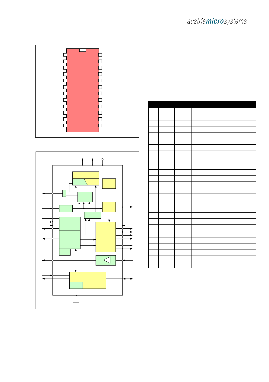
Figure 1
Pinout of AS8420
INTn
VBAT
VDD
VSS
WDOG
&
RESn
T MON
BUS I/F
TX
RX
SDO
STANDBY
BUS
SCK
RC OSC
VREG
RREF
LOGIC
SDI
SCSn
HIGH SIDE
DRIVERS
LOW SIDE
DRIVERS
CHAR
PUMP
POR
L SIDE
V-LIMIT
CURR
VREG
VBAT - VDD MON
VH
HG1
HS1
LG1
LG2
HG2
HS2
SENSE
VCP
CAMP
SPI I/F
Figure 2
Block Diagram of AS8420
Package Information
SOIC24
Pin Description, Pin Types
AIO
analog I/O
DO
digital output
DI
digital input
DO_OD digital output open drain
DIO_T digital I/O / tristate
S
supply pad
DI_PD digital input with pull-down
DO_T
digital output / tristate
Pin
Name
Type
Note
1 INTn
DO_T
Low active Interrupt signal
2 RESn
DO_OD
Reset - open drain
3 SCK
DI_PD
Serial Clock from µ C
4 SCSn
DI_PU
Low active Chip Select signal (1)
5 RREF
AIO
Reference Resistor for RC
Oscillator
6 VSS
S
Power Ground
7 VDD
S
5 V power supply
8 RX
DO
Bus transmission output
9 TX
DI_PU
Bus transmission input (1)
10 BUS
AIO
Bus line
11 VBAT
S
Battery Voltage (diode protected)
12 VREG
AIO
regulated supply - if ext. transistor
is not used, shorted to VDD
13 LG2
AIO
Output Gate LS driver 2
14 LG1
AIO
Output Gate LS driver 1
15 VCP
AIO
Output Charge Pump
16 VH
AIO
Charge Pump voltage (capacitor)
17 HG1
AIO
Output Gate HS driver 1
18 S1
AIO
Output Source HS driver 1
19 HG2
AIO
Output Gate HS driver 2
20 S2
AIO
Output Source HS driver 2
21 SENSE AIO
Analog input current measurement
22 CURR
AIO
current measurement output
23 SDI
DI
Serial Data In
24 SDO
DO_T
Serial Data Out
Table 1
Pinlist of AS8420
Note 1:
In case external VDD is below Vfuvdd threshold
SPI I/F and LIN Failure detection unit are inactive
Note 2:
During sleep mode this pin is clamped to VSS by
switching on a pull down resistor, that is normally
OFF
Note 3:
During sleep mode RX output is switched Low to
prevent circuitry from reverse supply of
µ Controller
AS8420
Revision No. 0., Date 2001-10-12
Page 3 of 9
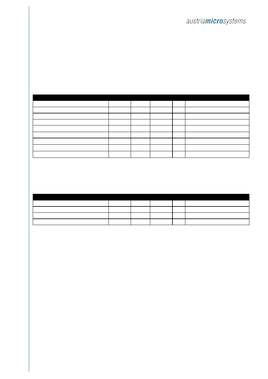
Electrical Parameters
Absolute Maximum Ratings (NON OPERATING)
Stresses beyond those listed under "Absolute Maximum Ratings" may cause permanent damage to the device. These are stress
ratings only. Functional operation of the device at these or any other conditions beyond those indicated under "Operating
Conditions" is not implied. Exposure to absolute maximum rating conditions for extended periods may affect device reliability.
Parameter
Symbol
Min
Max
Unit
Note
Battery voltage
VBAT
-0.3
20
V
(1) 42V for 400ms
Low Power Supply Voltage
VDD
-0.3
7
V
(1)
Input Pin Voltage
Vin
-0.3
VDD/V+0.3 V
Input Current (latchup immunity)
Iscr
-100
100
mA
Norm: Jedec 17
ESD
±1
kV
Norm: MIL 883 E method 3015
Total Power dissipation
Pt
300
mW
Storagetemperature
Tstrg
-55
125
∞C
Soldering conditions
Tlead
235
∞C
Norm: IEC 61760-1
Humidity non-condensing
5
85
%
Table 2
Absolute Maximum Ratings
Note 1:
Value of these process dependent parameters to be taken from according Process Parameter document, current
version
Operating Conditions
Parameter
Symbol
Min
Max
Unit
Note
Battery voltage
VBAT
7
18
V
(1)
Low Power Supply Voltage
VDD
4.75
5.25
V
(2)
Voltage drop on ground potential
VSS≠GND
-0.1
0.1
V
Ambient temperature
Tamb
-40
85
∞
C
Table 3
Operating Conditions
Note 1:
Load dump 42V
Note 2:
Recommended external capacitors
100nF
20 mA max. load, higher current with external transistor
AS8420
Revision No. 0., Date 2001-10-12
Page 4 of 9
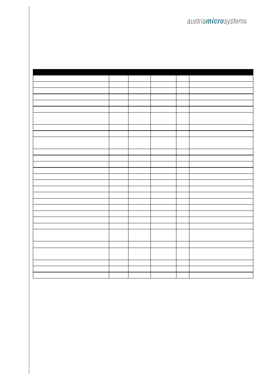
Characteristics for Analog and Digital Inputs and Outputs
Operational Parameters
Parameter
Symbol
Min
Max
Unit
Note
Charge Pump Voltage
VCP
VBAT/V+5
VBAT/V+12
V
(1) typ. VBB/V + 10 V
HS gate driver source current
IHS_so
-100
25
mA
(2) + (3)
HS gate driver sink current
IHS_si
25
100
mA
(2) + (3)
LS gate driver source current
ILS_so
-100
25
mA
(2) + (3)
LS gate driver sink current
ILS_si
25
100
mA
(2) + (3)
Oscillator frequency
fOSC
480
800
kHz
OnChip
PWM frequency
fPWM1
fPWM2
15
8
25
12
kHz
(4) typ 20 kHz
(5) typ 10 kHz
PWM resolution
resPWM
bit
typ. 5
PWM duty cycle
Dr
10
100
%
(6)
Dead Time for secure synchronous
rectification
tdelay
2
5
µ s
(7) typ. 3
Motor current measurement error
Evcurr
-10
10
%
Threshold for motor over current detection
Voc
mV
(8) typ. 500mV
Under Voltage VBAT
Vfuv
7
7.9
V
(9) + (10)
Over Voltage VBAT
Vfov
18
20
V
(9) + (10)
Under Voltage VDD
Vfuvdd
0,8*VDD
0,9*VDD
V
(9) + (10)
Over Voltage VDD
Vfovdd
1,1*VDD
1,2*VDD
V
(9) + (10)
Watchdog signal pulse width
twdres
10
40
us
(11) active low
Watchdog time out period
twdtrig
1.0
2.3
s
(12) typ. 1.5 sec
switch off delay
tsw_off
1
2
ms
(7)
dead time after VBAT Fault
td_FBAT
2
ms
(7)
Temperature threshold warning
TW
∞ C
(13) typ. 140
Temperature threshold Vreg
TOff
160
∞ C
(13)
Standby Current
IDD
100
µ A
(14)
Gain of Current Amplifier
gCAmp1
gCAmp2
(15) typ. 10
(15) typ. 15
Value of external Reference resistor
Rref
k
±1 % typ 22
reset active time after Power On or
WakeUp
tRES1
200
ms
(7)
reset active time before Power Off
tRES2
1
ms
(7)
Debounce Time of internal signals
tdeb2
µ s
(7) typ. 30
MOSFET driver current control
Irramp
25
100
µ s
Internal current ref.
Table 4
analog signal parameters
Note 1:
External capacitors C > 200 nF recommended, Lower threshold > 8 V according to VBB Monitor.
Note 2:
Typical rise/ fall time at the Power MOSFET gate: 1 µ s.
Note 3:
Recommended Power MOSFET STB80NE06L-10, Gate approx. 7,6nF/ model, RDSon = 0,01
.
Note 4: epending on value of reference resistor.
Note 5:
Depending on settings of Global Control Register, bit PWMF.
Note 6:
Programmable via SPI I/F.
Note 7: nternal time base.
Note 8:
Rsens value depends on motor current.
Note 9:
Interrupt becomes active.
Note 10: 250 mV hysteresis.
AS8420
Revision No. 0., Date 2001-10-12
Page 5 of 9
Note 11: Active low digital output triggered by Watch Dog overflow.
Note 12: Digital input from microprocessor within a time between 200 and 1000 ms.
Note 13: Hysteresis > 10 grd.
Note 14: Voltage regulator, internal oscillator NOT running, 25 ∞ C, VBAT = 14 V.
Note 15: Depending on setting of Global Control Register, bit GAIN.
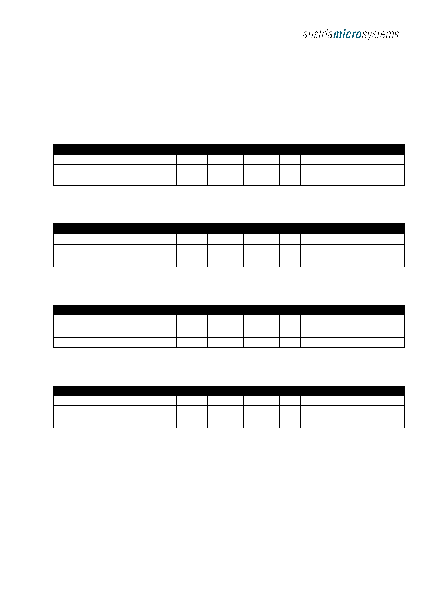
CMOS Input
Parameter
Symbol
Min
Max
Unit
Note
High Level Input Voltage
VIH
0.7 * VDD
V
Low Level Input Voltage
VIL
0.3 * VDD
V
Input Leakage Current
ILEAK
1
µA
Table 5
CMOS Inputt parameters
CMOS output
Parameter
Symbol
Min
Max
Unit
Note
High Level Output Voltage
VOH
VDD/V-0.5
V
Low Level Output Voltage
VOL
VSS/V+0.4
V
Capacitive Load
CL
50
pF
Table 6
CMOS outtput parameters
Tristate CMOS output
Parameter
Symbol
Min
Max
Unit
Note
High Level Output Voltage
VOH
VDD/V-0.5
V
Low Level Output Voltage
VOL
VSS/V+0.4
V
Trisate Leakage Current
IOZ
1
µA
to VDD and VSS
Table 7
Tristate CMOS outtput parameters
CMOS open-drain output
Parameter
Symbol
Min
Max
Unit
Note
Low Level Output Voltage
VOL
0.4
V
IOL = 4mA
Open drain leakage current
ILEAK
-10
10
µA
Capacitive Load
CL
50
pF
Table 8
CMOS open-drain parameters

AS8420
Revision No. 0., Date 2001-10-12
Page 6 of 9
MicroController Interface
Registerfile
ADDRESS - hexadecimal
Name
ACCESS
Description
00
GCR1
R/W
Global Control Register 1
01
GCR2
R/W
Global Control Register 2
02
PSR
R/W
PWM SetUp Register
03
FDR
R/W
FailureDetection Register
04
TST
R/W
Test Mode Register
05
MSK
R/W
Interrupt Mask Register
07
MRR
R
Mask Release Register
Table 9
Registerfile description
SPI Interface
Data transfer from the microprocessor to the ASIC and vica versa is accomplished by means of a SPI interface. For a detailed
description of the SPI-interface features please refer to [SPI].
Physical Interface
Supported modes, and bit order are shown in Figure 3. Only modes that conform to CPHA=1 (see [SPI]) are supported. With this
mode the output shift operation always takes place before the input sample operation. The clock polarity is fix CPOL = 0. The
MSB is always transmitted / received first.
SCSn
SCK
(CPOL=0)
SDI
SDO
MSB
MSB
LSB
LSB
Figure 3
SPI - Physical interface
Communication Protocol
The SPI-interface acts as communication interface between the µ Controller and the registers within the Single Motor H-Bridge
Controller. For efficient register access, a protocol has been defined with the following features:
∑
Purely master-slave protocol with µ Controller as master
∑
Only one register accessible within one telegram
∑
Two different frames: One read and one write frame
∑
Frame is delimited by the status of SCSn (SCSn = frame delimiter)

AS8420
Revision No. 0., Date 2001-10-12
Page 7 of 9
Application Note
HG
a
t
e
1
Sr
c
1
LG
at
e
1
P
I
C
16F
877
QF
P
4
4
R1
1
R5
HG
a
t
e
1
Sr
c
1
LG
ate
1
C
p
Cs
VD
1
HG
a
t
e
2
LG
ate
2
VB
A
T
Sr
c
2
M
R6
R7
R9
R8
VD
4
VD
5
VD
2
+
VD
3
VD
D
VS
S
AN
1
SD
I
SD
O
42
43
8
IN
T
18
MC
L
R
/
V
p
p
37
SC
K
24
SS
20
6
7
1
44
TX
RX
C1
C2
VD
6
Qp
r
o
t
+
C4
RV
R3
PG
M
PG
C
PG
D
R2
LV
_P
R
O
G
R
A
M
P
G
C/
HA
L
L
-
PG
D
/
H
A
L
L
+
BU
S_
L
I
N
11
16
17
AN
0
19
R1
2
R1
3
GN
D
13
14
24
23
22
21
20
19
18
17
16
15
A
S
8
420
10
1
2
3
4
5
6
7
8
9
11
12
VR
E
G
RE
S
n
RR
e
f
BU
S
TX
RX
VD
D
VB
A
T
VS
S
IN
T
n
SC
K
SC
Sn
VC
P
VH
HG
2
S2
LG
1
HG
1
LG
2
S1
SE
N
S
E
CU
RR
SD
I
SD
O
13
14
24
23
22
21
20
19
18
17
16
15
C3
C4
+
Figure 4
full configuered µ Controller driven system

AS8420
Revision No. 0., Date 2001-10-12
Page 8 of 9
MARKING / PACKAGE - PRODUCTION PARTS
Package type:
SOIC24
E
H
1 2 3
A
A1
e
b
L
Figure 5
SOIC24 Package
D
E
H
A
A1
e
b
L
Copl.
min
max
15.20
15.60
7.40
7.60
10.00
10.65
2.35
2.65
0.1
0.30
1.27
0.33
0.51
0.40
1.27
0.10
0 ∞
8 ∞
Table 10
Package Dimensions
Marking: YYWWIZZ
YY
year
WW
week
I
plant identifier
ZZ
letters of free choice
AS8420
10
1
2
3
4
5
6
7
8
9
11
12
13
14
24
23
22
21
20
19
18
17
16
15
YYWWIZZ
Figure 6
Package Marking

AS8420
Revision No. 0., Date 2001-10-12
Page 9 of 9
Contact
austriamicrosystems AG
Desiree Herz
A 8141 Schloss Premst‰tten, Austria
T. +43 (0) 3136 500 5818
F. +43 (0) 3136 500 5811
drive@austriamicrosystems.com
Copyright
Devices sold by austriamicrosystems are covered by the
warranty and patent indemnification provisions appearing
in its Term of Sale. austriamicrosystems makes no
warranty, express, statutory, implied, or by description
regarding the information set forth herein or regarding the
freedom of the described devices from patent infringement.
austriamicrosystems reserves the right to change
specifications and prices at any time and without notice.
Therefore, prior to designing this product into a system, it
is necessary to check with austriamicrosystems for current
information.
This product is intended for use in normal commercial
applications. Applications requiring extended temperature
range, unusual environmental requirements, or high
reliability applications, such as military, medical life-
support or life-sustaining equipment are specifically not
recommended without additional processing by
austriamicrosystems for each application.
Copyright © 2001 austriamicrosystems. Trademarks
registered Æ. All rights reserved. The material herein may
not be reproduced, adapted, merged, translated, stored, or
used without the prior written consent of the copyright
owner. To the best of its knowledge, austriamicrosystems
asserts that the information contained in this publication is
accurate and correct.