 | –≠–ª–µ–∫—Ç—Ä–æ–Ω–Ω—ã–π –∫–æ–º–ø–æ–Ω–µ–Ω—Ç: AS8500 | –°–∫–∞—á–∞—Ç—å:  PDF PDF  ZIP ZIP |

1.1
2
3
DATA SHEET
Revision 1.1, 04-April-06 www.austriamicrosystems.com Page 1 of 39
1
Features
16 bits resolution
differential inputs
Single + 5V supply
Low power 15 mW
SOIC16 package
Self- and system-calibration
with auto-calibration on power up
16 kHz maximum sampling frequency
internal temperature measurement
internal reference
programmable current sources
digital comparator
active wake-up
PGA gains 6, 24, 50, 100
Zero offset
Zero offset TC
Extremely low noise
Internal oscillator with comparator for active wake up
3-wire serial interface,
P compatible
temperature range ≠ 40 to + 125 ∞C
2
Applications
battery management for automotive systems
power management
mV/µV-meter
thermocouple temperature measurement
RTD precision temperature measurement
high-precision voltage and current measurement
3
General description
The AS8500 is a complete, low power data acquisition system
for very small signals (i.e. voltages from shunt resistors,
thermocouples) that operates on a single 5 V power supply. The
chip powers up with a set of default conditions at which time it
can be operated as a read-only-converter. Reprogramming is at
any time possible by just writing
into two internal registers via
the serial interface.
The AS8500 has four ground refering inputs which can be
switched separately to the internal PGA. Two input channels can
also be operated as a fully differential ground free input. The
system can measure both positive and negative input signals.
The PGA amplification ranges from 6 to 100 which enables the
system to measure signals from 7mV to 120 mV full scale range
with high accuracy, linearity and speed.
The chip contains a high precision bandgap reference and an
active offset compensation that makes the system offset free
(better than 0,5
V) and the offset-TC value negligible. The built-
in programmable digital filter allows an effective noise
suppression if the high speed is not necessary in the application.
The input noise density is only 35 nV / Hz and due to
the high internal chopping frequency the system is free of 1/f-noise down
to DC.The 0-10 Hz noise is typical below 1 µV i.e. as good or better than
any other available chopper amplifier.
For high speed synchronous measurements the chip can run in an
automatic switching mode between two input channels with pre-
programmed parameter sets.
The circuit has been optimised for the application in battery management
systems in automotive systems. As a front end data acquisition system it
allows an high quality measurement of current, voltage and temperature
of the battery.
With a high quality 100
resistor the system can handle the starter
current of up to 1500 A, a continuous current of
± 300 A as well as the
very low idle current of a few mA in the standby mode.
For external temperature measurement the chip can use a wide variety of
different temperature sensors such as RTD, PTC, NTC, thermocouples or
even diodes or transistors. A built-in programmable current source can be
switched to any input and activate these sensors without the need of
other external components.
The measurement of the chip temperature with the integrated internal
temperature sensor allows in addition the temperature compensation of
sensitive parameters which increases the total accuracy considerably.
The flexibility of the system is further increased by a digital comparator
that can be assigned to any measured property
(current, voltage, temperature) and an active wake-up in the sleep-mode.
All analog input-terminals can be checked for wire break via the SDI-
interface.
INTERNAL TEMPERATURE
INPUT MUX
CHOPPER
PROTECTION
CURRENT
SOURCES
ETR
ETS
RSHH
RSHL
VBAT
16 BIT - CONVERTER
BUF
SERIAL INTERFACE / CONTROL REGISTERS
DSP
CONTROLLER
FILTER
INT. CLOCK
TIMER
CALIBRATION
DATA
COMPARATOR
1.26 V
REFERENCE
SCLK
SDAT
INTN
REF
AGND
VDDA
VSSA
VDDD
VSSD
CLK
EZPRG
PGA
and
LEVEL SHIFT
AS8500
Preliminary
Data Sheet
Universal multi pupose data aquisition system
Figure 1: Functional Block Diagram

AS8500 - Preliminary Data Sheet
austriamicrosystems
Revision 1.1, 04-April-06 www.austriamicrosystems.com Page 2 of 39
CONTENTS
1
FEATURES.........................................................................................................................................................................................1
2
APPLICATIONS .................................................................................................................................................................................1
3
GENERAL DESCRIPTION.................................................................................................................................................................1
4
PIN FUNCTION DESCRIPTION FOR SOIC 16 PACKAGE...............................................................................................................3
5
ABSOLUTE MAXIMUM RATINGS.....................................................................................................................................................4
6
ELECTRICAL CHARACTERISTICS..................................................................................................................................................5
7
FUNCTIONAL DESCRIPTION ...........................................................................................................................................................9
7.1
P
OWER ON
R
ESET
...........................................................................................................................................................................9
7.2
A
NALOG PART
,
GENERAL DESCRIPTION
.............................................................................................................................................9
7.2.1
Reference voltage .............................................................................................................................................................10
7.2.2
Current sources.................................................................................................................................................................11
7.2.3
Internal temperature sensor ..............................................................................................................................................12
7.3
D
IGITAL PART
.................................................................................................................................................................................12
7.3.1
Sampling rate ....................................................................................................................................................................12
7.3.2
Calibration .........................................................................................................................................................................12
7.4
M
ODES OF OPERATION
...................................................................................................................................................................13
7.5
R
EGISTER DESCRIPTION
.................................................................................................................................................................14
7.5.1
OPM operation mode register ( 4 bits ) .............................................................................................................................15
7.5.2
CRG general configuration register ( 28 bits )...................................................................................................................15
7.5.3
CRA measurement channel A configuration register ( 17 bits ) ......................................................................................16
7.5.4
CRB measurement channel B configuration register ( 17 bits ) .......................................................................................18
7.5.5
ZZR Zener-Zap register (188 bits ):..................................................................................................................................19
7.5.6
CAR calibration register ( 110 bits ) .................................................................................................................................21
7.5.7
TRR trimming register ( 20 bits ) .......................................................................................................................................21
7.5.8
THR alarm (Wake-up) threshold register ( 17 bits ) .........................................................................................................24
7.5.9
MSR measurement result register ( 18 bits )....................................................................................................................24
8
DIGITAL INTERFACE DESCRIPTION.............................................................................................................................................24
8.1
CLK..............................................................................................................................................................................................24
8.2
INTN ............................................................................................................................................................................................24
8.3
SDI
BUS OPERATION
......................................................................................................................................................................25
8.4
D
ATA TRANSFERS
..........................................................................................................................................................................26
8.5
SDI
BUS TIMING
.............................................................................................................................................................................27
8.6
SDI
ACCESS TO
OTP
MEMORY
........................................................................................................................................................28
8.6.1
ZZR register bit mapping...................................................................................................................................................28
8.6.2
Stored ZZR-register mapping............................................................................................................................................32
9
GENERAL APPLICATION HINTS ...................................................................................................................................................33
9.1
G
ROUND CONNECTION
,
ANALOG COMMON
.......................................................................................................................................33
9.2
T
HERMAL
EMF ..............................................................................................................................................................................33
9.3
N
OISE CONSIDERATIONS
.................................................................................................................................................................33
9.4
S
HIELDING
,
GUARDING
....................................................................................................................................................................34
10
TYPICAL PERFORMANCE CHARACTERISTICS ..........................................................................................................................35
11
PACKAGE DIMENSIONS ................................................................................................................................................................37
12
REVISION HISTORY........................................................................................................................................................................37
13
ORDERING INFORMATION ............................................................................................................................................................37
14
CONTACT.........................................................................................................................................................................................38
14.1
H
EADQUARTERS
.......................................................................................................................................................................38
14.2
S
ALES
O
FFICES
........................................................................................................................................................................38
AS8500 - Preliminary Data Sheet
austriamicrosystems
Revision 1.1, 04-April-06 www.austriamicrosystems.com Page 3 of 39
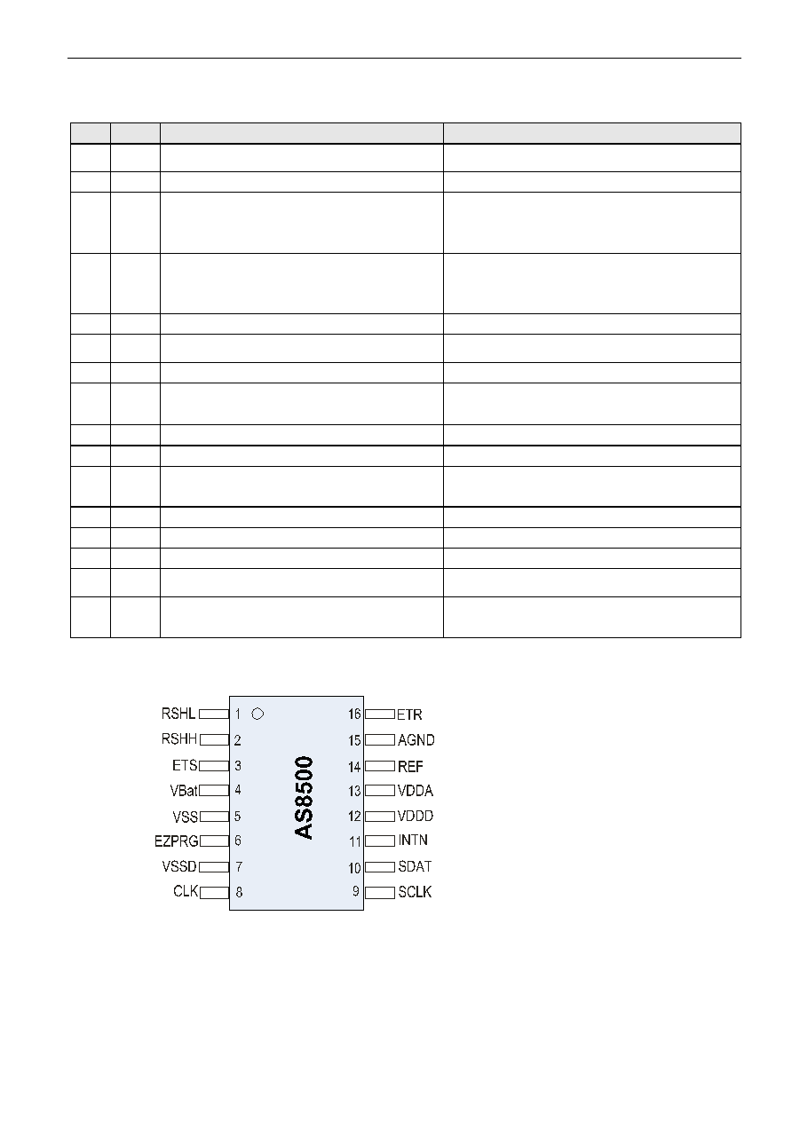
4
PIN function description for SOIC 16 package
PIN
Name
description
Comment
1
RSHL
anlalog input from shunt resistor low side
analog common for VBAT, ETS and ETR; return for internal
current source
2
RSHH
anlalog input from shunt resistor high side
3
ETS
analog input with reference to RSHL
analog input for differential input ETS-VBAT
analog output for current-source
4
VBAT
analog input with reference to RSHL
analog input for differential input ETS-VBAT
analog output for current-source
5 VSS 0V-power
supply for analog part
6
EZPRG digital power input for programming Zener fuses.
This input must be open or connected to VDDD. It is not intended,
that OTP content is modified by the user.
7 VSSD
0V-power
supply
and ground reference point for digital part
8
CLK
digital input for external clock, master clock input
external clock typical 8.192 MHz; during MWU-mode (see 7.4)
external connection must be high impedance or connected to
VDDD to reduce current consumption
9
SCLK
serial port clock input for SDI-port
the user must provide a serial clock on this input
10
SDAT
serial data in- and output
11
INTN
Digital I/O for interrupt from comparator
signal wake-up to external µC
conversion ready flag for external interupt and synchronisation in normal mode
12
VDDD
+ 5V digital power supply
13
VDDA
+ 5V analog power supply
14
REF
reference input/output
must be connected to VSS with a 30 nF capacitor
15
AGND
analog ground, ground reference for ADC
this PIN must be connected with a 50-100nF-capacitor to VSS;
no direct connection to VSSD/VSS allowed
16
ETR
analog input with reference to RSHL
analog output for current-source
Table 1: Pin Description
Figure 2: Schematic Package outline SOIC 16

AS8500 - Preliminary Data Sheet
austriamicrosystems
Revision 1.1, 04-April-06 www.austriamicrosystems.com Page 4 of 39
5
Absolute Maximum Ratings
Stress beyond those listed under "Absolute Maximum Ratings" may cause permanent damage to the device. These are stress ratings only. Functional
operation of the device at these or any other conditions beyond those indicated under "Operating Conditions" is not implied. Exposure to absolute
maximum rating conditions for extended periods may affect device reliability. All voltages are defined with respect to VSS and VSSD. Positive currents
flow into the IC.
Absolute maximum ratings (T
A
= -40∞C to 125∞C unless otherwise specified)
Nr.
PARAMETER
SYMBOL
MIN
TYP
MAX
UNIT
NOTE
0 Supply
voltage
Analogue VDDA and digital VDDD
VDD
-0.3 7.0
V
Polarity
inversion
externally
protected
1
Input pin voltage
Vin
-0.3
VDD
+0.3
V
2
Input current
(latch-up immunity)
I
SCR
-100
100
mA
JEDEC 17
3 Electrostatic
discharge
ESD
-2
2
kV
1)
4 Ambient
temperature
T
A
-40 125
O
C
(Tj = 150∞C)
5 Storage
temperature
T
STRG
-55 150
O
C
6 Soldering
conditions
T
LEAD
260
∞C
2)
7 Humidity,
non-condensing
5
85 %
8 Thermal
resistance
R
thJA
75
K/W
9 Power
dissipation
P
TOT
350
mW
Notes:
1)
MIL 883 E method 3015, HBM: R =1.5 k
, C =100pF.
2)
Jedec Std ≠ 020C, lead free

AS8500 - Preliminary Data Sheet
austriamicrosystems
Revision 1.1, 04-April-06 www.austriamicrosystems.com Page 5 of 39
6
Electrical characteristics
VDDA=5V +/-0.1 V, fclk=8.192 MHz, chopping ratio MM=4 (see 7.5.3), oversampling frequency=2.048 MHz, oversampling ratio=128
temperature range : -40 to 125∞C if not otherwise noted
symbol
parameter
conditions
min
typ
max
units
input characteristics
G1
for gain 1 the input signal is connected directly to th input of the converter, this is not possible for the RSHH-RSHL
input
Gain
gains of PGA
6, 24, 50, 100
1)
AC_g6
Accuracy at gain 6
0 to 85 ∞C
0.4
% @-120mV
2)
-40 to 125∞C
1.0
% @-120mV
2),3)
AC_g24
Accuracy at gain 24
0 to 85 ∞C
0.2
% @+-20mV
2)
-40 to 125∞C
0.6
% @+-20mV
2) 3)
AC_g50
Accuracy at gain 50
0 to 85 ∞C
1
% @+-10mV
2)4)
AC_g100
Accuracy at gain 100
0 to 85 ∞C
1
% @+-5mV
2)4)
Vin
input voltage ranges
G1
-300 to + 800
mV
5)
(with reference to RSHL)
G6
+/- 120
mV
6)
G24
+/- 30
mV
6)
G50
+/- 15
mV
7)
G100
+/- 7.5
mV
7)
Notes:
1)
the absolute gain values are subjected to a manufacturing spread of +/-30%
2)
Accuracy relies on bandgap characteristic, on the gain variation over temperature and on the trimm information. To achieve optimum performance,
the circuit may be trimmed by the user for best temperature stability by writting aproporiate data to the TRR register (see sections 7.4 and 7.5)
Default content of TRR register is 17.
3)
due to a nonlinear behaviour of the gain and reference voltage over temperature the accuracy is lower for the extended temperature range.
4)
It is recommended to use these gain settings only for applications in the temperature range 0 t0 85∞C
therefore it is recommended to use these gain settings only for applications in the temperature range 0 to 85∞C.
5)
this gain range is not using the internal PGA, the input is directely connected to the AD-converter. Therefore the input resistance is lower then for
other gain ranges.
It has been designed mainly for positive input voltages up to 0.8 V i.e. for measurements of temperature with transistors and diodes.
The limitation for negative input voltages is due to the onset of conduction of the input protection diodes.
6)
the ASIC is optimised for G6 and G24 concerning linearity, speed and TC, therefore these ranges are recommended whenever possible.
7
) because of higher TC value at elevated temperature G50 and G100 are recommended for applications in the temperature range 0 to 85∞C

AS8500 - Preliminary Data Sheet
austriamicrosystems
Revision 1.1, 04-April-06 www.austriamicrosystems.com Page 6 of 39
Electrical characteristics (continued)
VDDA=5V +/-0.1 V, fclk=8.192 MHz, chopping ratio MM=4 (see 7.5.3), oversampling frequency=2.048 MHz, oversampling ratio=128
temperature range : -40 to 125∞C if not otherwise noted
symbol
parameter
conditions
min
typ
max
units
cal_err
calibration error
for 30 000 digits output at
full range
G1, 720 mV
G6, 120 mV
G24, 30 mV
G50, 15 mV
G100, 7.5 mV
Device is not
factory
calibrated
%
1)
lin_err
nonlinearity
gain 6 @ room temp
0.1
% or 30 digits
2)
gain 24 @ room temp
0.03
% or 10 digits
2)
gain 50 @ room temp
0.05
% or 15 digits
2)
gain 100 @ room temp
0.05
% or 20 digits
2)
lin_errTC
TC of linearity error
all gains
1
5
ppm/K
3)
Vos
offset voltage:
RSHH_RSHL
-40 to 125∞C
-0.5
0.2
0.5
µV
4)
offset voltage: ETS, ETR,
VBAT
-40 to 85∞C
-2
0.5
1
µV
4)
85 to 125∞C
-4
1
2
µV
4)
dVos/dT
Offset voltage drift: RSHH-
RSHL
-40 to 85 ∞C
0.002
µV/K
Ib
input bias/leakage current,
all channels
room temperature
-1000
0.2
1000
nA
5)
Vndin
voltage noise density
(G=24)
f=0 to 1 kHz
35
50
nV//Hz
6)
Indin
current noise density
(G=24) f=10
Hz
20
fA//Hz
6)
en p_p
voltage noise, peak (G=24) 0 to 100 Hz
3
µV
6)
0 to 10 Hz
1
µV
6)
en_RMS
voltage noise, RMS (G=24) 1000 Hz
1.5
µV
6)
SNR
signal to noise (G=24, G=6) room temperature
100
dBmin
SDR
signal to distortion (G=24,
G=6)
room temperature
100
dBmin
CCI
chanel to chanel insulation room temperature
-90
dBmax
PSRR
power supply rejection ratio 4.9 to 5.1 V
-60
dBmax
Notes:
1)
The output response might be calibrated by the user by writing appropriate calibration constants to the CAR register (see 7.5. ). The default values
are 1548 dec
2)
whatever is lower
3)
max limit is derived fromdevice characterization and not tested
4)
Min/Maximum limits over temperature range are derived from device characterization and not etsted. In normal operation a termperature independent
digital offset of -0.7 digits is present due to internal raunding.
5)
Typical leakage current is valid for all gain settings except G=1 for positive input voltages below 200 mV. In the temperature range 85-125∞C it may
be as high as 5 nA. In normal operation a temperature independent digital offset of -0.7 digits is present due to internal rounding.
6)
This parameter is not measured directly. It is measured indirectly via gain measurement of the whole path at room temperature

AS8500 - Preliminary Data Sheet
austriamicrosystems
Revision 1.1, 04-April-06 www.austriamicrosystems.com Page 7 of 39
Electrical characteristics (continued)
VDDA=5V +/-0.1 V, fclk=8.192 MHz, chopping ratio MM=4 (see 7.5.3), oversampling frequency=2.048 MHz, oversampling ratio =128
temperature range : -40 to 125∞C if not otherwise noted
symbol
parameter
conditions
min
typ
max
units
data conversion
RES
resolution
all channels
16
bits
1) 2)
Vref
reference voltage
room temperature
1.21
V
Vref_TC
temperature coefficient of Vref
0-85∞C,box
method
20
ppm/K
3)
Vref_Ri
internal resistance of Vref
Rload > 50 kOhm
200
Ohm
fovs
clock frequency
4.096
MHz
R1
oversamplig ratio
64
128
MM
conversions during chopper cycle
4
8
BW bandwidth
7.8
1000
16000
Hz
av
internal averaging
1
4
1024
cycles
fclk
external clock frequency
0.05
8.192
10
MHz
4)
CLK_extdiv
clock division factor
2
4
DR_clk
duty ratio of external clock
50
%
int_fclk
internal clock frequency
180
250
330
kHz
analog inputs
RSHH, VBAT, ETS, ETS
Rin
input resistance
Ue < 150 mV
50
100
MOhm
Cin
input capacitance at gain 24
8
15
30
pF
internal temperature sensor
T_out20
output at 23∞C
G 6, typical
23 000
digits
T_sl
slope
-20 to 100∞C
75
digits/degC
current source
output to RSHH, RSHL
Icurr_rshh
2
µA
Notes:
1)
with external averaging the resolution can be increased up to 21 bits with an effective sampling rate below 10 Hz
2
) the system works in overflow condition without degradation of accuracy up to 1.4 * range width.
This means that the overflow bit can work as bit no.17 in this range.
3)
TC- value of the reference voltage may be set through trimm bits intentionally higher to minimize TC of the entire measurement path for gain 24
4)
in the temperature range 0 - 85∞C the clock frequency can be increased to 12 MHz

AS8500 - Preliminary Data Sheet
austriamicrosystems
Revision 1.1, 04-April-06 www.austriamicrosystems.com Page 8 of 39
Electrical characteristics (continued)
VDDA=5V +/-0.1 V, fclk=8.192 MHz, chopping ratio MM=4 (see 7.5.3), oversampling frequency=2.048 MHz, oversampling ratio=128
temperature range : -40 to 125∞C if not otherwise noted
symbol
parameter
conditions
min
typ
max
units
programmable current source
output to Vbat, ETS, or ETR
Icurr_ON
current level
0
248
µA
I_steps
current steps
6
8
10
µA
TC_CS
temperature coefficient
900
ppm/K
Icurr_OFF
current when off
room temperature
0.001
µA
Icurr_Ri
internal resistance of current source Ua < 2 V
10
MOhm
digital CMOS inputs with pull up and schmidt-trigger
input PINs CLK and SCLK
Vih
high level input voltage
VDDD=5V
3.5
V
Vil
low level input voltage
VDDD=5V
1.5
V
Iih
current level
VDDD=5V, Vih=5V
-1
1
µA
Iil
current level
VDDD=5V, Vil=0
30
120
µA
digital CMOS outputs
output PINs SDAT and INTN
Voh
high level output voltage
VDDD=5V, -633uA
4.5
V
Vol
low level output voltage
VDDD=5V, 564uA
0.4
V
Cl
capacitive load
20
pF
Tristate digital I/O
Voh
high level output voltage
VDDD=5V, -633uA
4.5
V
Vol
low level output voltage
VDDD=5V, 564uA
0.4
V
Ioz
tristate leakage current to
VDDD,VSSD
VDDD=5V
-1
1
µA
Vih
high level input voltage
VDDD=5V
3.5
V
Vil
low level input voltage
VDDD=5V
1.5
V
supply current
Isup normal
operation
VDDD=VDDA=5V
3
5
mA
Iaw
active wake-up
VDDD=VDDA=5V
40
100
µA
1)
supply voltage
VDDA
positive analog supply voltage
4.7
5.0
5.3
V
2)
VDDD positive
digital
supply voltage
4.5
5.0
5.5
V
VSS, VSSD
negative supply voltage
0
V
Power On Reset
Vporhi
Power on reset Hi
3.1
V
Vhyst
Hysteresis
0.2
V
Notes:
1)
the average current is dependent on the on-time of the measurement system i.e. it can be programed via the CRA register
2)
dynamic stability of analog supply should be within +/- 0.1 V

AS8500 - Preliminary Data Sheet
austriamicrosystems
Revision 1.1, 04-April-06 www.austriamicrosystems.com Page 9 of 39
7
Functional Description
7.1
Power on Reset
The power on reset is iniciated during each power up of the ASIC and can be triggered purpously by reducing the analog supply voltage (VDDA) to a
value lower than Vporlo for a time interval longer than 0.5 µsec.
During power on reset sequence the following steps are performed automatically:
-
The chip goes to mode MZL (see 7.4)
-
Internal clock is enabled
-
The calibration constants are loaded from Zener-zap memory to the appropriate registers (ZTR=>TRR, ZCL=>CAR). The load procedure is
directed by the internal clock and can be monitored on INTN pin. 188 clock pulses are generated from the internal oscillator source. Pulse period
is equal to internal clock period.
After the power-on reset sequence is finished:
-
the operation continues with internal clock if no external clock is detected. In this case the ASICs switches to mode MWU with default value of
threshold register ( 2
14
)
-
If external clock is available the ASIC switches to mode current measurement MMS (default measurement with default configuration: gain=100,
fovs=4.096MHz, R1=64, MM=4, R2=1, N
TH
=2
14
).
-
The microcontroller can communicate via SDI interface whenever appropriate, i.e. CAR and TRR register can be rewritten from the µC if
necessary.
-
Because the automatic selected calibration factor (CGI4) is loaded with zeros, the ASIC delivers constant zero at the output to allow the µC to
check for an unwanted POR. To bring the ASIC back into normal operation for current
measurement with gain100 the µC has to copy the CAU4 default content or a customer specific calibration factor into the CAR-register.
(see also 7.5.5 and 8.6.2)
7.2
Analog part, general description
The input signals are level shifted to AGND (+ 2.5 V) then switched by the special high quality MUX- which contains also the chopper ≠ to the input of
the programmable gain amplifier (PGA). This low noise amplifier is optimised for best linearity, TC- value and speed at gain 24.
The systems contains an internal bandgap reference with high stability, low noise and low TC-value. The output of a programmable current source can
be switched to the analog inputs VBAT, ETS and ETR for testing the sensor connections
or for external activation of resistors, bridges or sensors (RTD, NTC). The voltage drop generated by the current is measured at the corresponding
input/output PIN.
For the wire break test of the RSHH and RSHL inputs special low noise current sources are implemented.
The integrated temperature sensor can also be switched to the PGA by the MUX and measured any time. The chip temperature can be used for the
temperature compensation of
the gain of the different channels in the external µC, which increases the absolute accuracy considerably.
The offset of the amplifier itself is already fairly low, but to guarantee the full dynamic range it can be trimmed via the digital interface to nearly zero
independent of the autozero
chopping function.
In the same way the manufacturing spread of the absolute value of the reference voltage can be eliminated and the TC-value set to nearly zero by a
trimming process via the SDI interface.
For more details of the input multiplexer see the following schematic. The position of all switches is defined by writing into the registers CRA, CRB and
CRG via the SDI bus, which is explained in 7.5.2 through 7.5.4.
INTERNAL
TEMPERA-
TURE
AD-
CON-
VERTER
PGA
AUXILIARY
CURRENT
SOURCE
M 12
M 13
M 3
M 10
M 14
CURRENT
SOURCE
M 2
M 1
M 4
M 15
M 8
M 7
M 9
M 6
ETR
ETS
VBAT
RSHH
RSHL
M 5
Figure 3: Multiplexer

AS8500 - Preliminary Data Sheet
austriamicrosystems
Revision 1.1, 04-April-06 www.austriamicrosystems.com Page 10 of 39
7.2.1
Reference voltage
The ASIC contains a highly sophisticated precision reference voltage. Its typical temperature dependence is a slight parabola shaped curve and is
shown in figure 14. This reference voltage is used mainly for the internal AD-converter, but can also be used for external purposes if the impedance of
the external circuitry is high enough.
The absolute value and its temperature coefficient (TC) is given by the content of the TRR register. This opens the possibility to calibrate the reference
voltage to the optimum absolute value (i.e. 1.28 V) and the TC value to zero thus eliminating fully the production spread.
Writing into subregister TRIMBV of TRR changes the absolute value linearly by 5.1 mV per digit as shown in the following graph and described in full
detail in 7.5.7
Trimming the TC value is similarly done by writing into subregister TRIMBTC. Since the TC trimming is also changing the absolute value it is important
to trim the TC first and then the absolute value.
as function of temperature
1,16
1,20
1,24
1,28
1,32
1,36
0
5
10
15
20
25
30
content of TRIMBV in bits
r
e
f
e
re
nce v
o
lt
a
g
e i
n
V
75 ∞C
24 ∞C
reference voltage as function of resistance load
1,12
1,14
1,16
1,18
1,20
1,22
1,24
1,26
10
20
30
40
50
60
70
80
90
100
110
resistance load in kOhm
r
e
f
e
ren
ce v
o
lt
ag
e
i
n
V
measurement
open loop value

AS8500 - Preliminary Data Sheet
austriamicrosystems
Revision 1.1, 04-April-06 www.austriamicrosystems.com Page 11 of 39
The TC trimming also opens the unique possibility to change the TC-value within the time of reprogramming of the TRR-register (i.e. within µsec) to
allow the compensation of
different TC-values of the external circuitry for different channels.
In addition it can be used for very fast autocalibration of the total TC of a given channel. An external reference voltage is applied to the channel to be
checked. Then all numbers from 0 to 31 are written into subregister TRIMBTC and a reading is done for the input voltage and the internal temperature
as well. The same is repeated at any temperature above RT. From these data the TRIMBTC setting for a minimum drift can be easily calculated.
7.2.2
Current sources
The AS8500 contains several current sources which can be used for checking all input lines for wire brake, to control external circuitry or to activate
external sensors.
Main current source
The main current source can be digitally controlled via the content of the CRG register in 31 steps of 8 µA in the range of 0 to 248 µV. Its absolute
value can be calibrated by writing in the subregister TRIMC of TRR.
The current source can be switched to the inputs VBAT, ETR or ETS to activate external sensors like RTDs, NTCs or resistance briges and strain
gages. It can also be used to detect a wire breake of external connected sensors. Performing a measurement with a high and a low (or zero) current
opens the possiblity to eliminate thermal EMF voltages in external sensors.
Secondary current sources
The ASIC contains two other high quality current sources supplying a current of approx. 2µA at the inputs RSHL and RSHH. These current sources can
be switched on and off at any time to check the correct connection of both terminals. During off state they must not interfere with the high sensitive
voltage inputs, especially the noise level should not be increased. If one of the terminals is an open connection the amplifier goes into saturation and
the overflow bit is set.
temperature coefficient as function of TRIMBTC setting
-250
-200
-150
-100
-50
0
50
100
150
200
0
5
10
15
20
25
30
35
setting of subregister TRIMBTC of TRR
t
e
m
p
er
at
ur
e co
ef
f
i
c
i
ent
i
n
ppm
/
K
change 12.7 ppm/K
per step

AS8500 - Preliminary Data Sheet
austriamicrosystems
Revision 1.1, 04-April-06 www.austriamicrosystems.com Page 12 of 39
7.2.3
Internal temperature sensor
The ASIC contains a high sensitive precision temperature sensor
which can be used at any time. The sensor supplies a very linear
voltage with temperature. The voltage can be measured using the
internal circuitry with gain 6, with free selection of all other parameters
defining the sampling rate.
The slope of the curve is approx. 75 digits per degC.
The calculation of the temperature has to be done in the external µC
acc. to the following simple formula:
Tint=( Uint(T)-Uint(23) ) / 75 + 23∞C
Uint(T) is the measured result and Uint(23) is the reference value at
23∞C, which is stored as an 11 bit-word in the ZZR-register.
7.3
Digital part
In the digital part the result of the AD-converter is processed, i.e.
calibration, active offset cancellation and filtering is done. In addition
the communication via the serial SDI interface is handled and all
circuit functions (like voltage and current path settings, chopping,
dechopping) are controlled.
Whenever the power supply line returns from below POR threshold a
power-up circuitry is activated which loads the internal calibration
registers from the Zener-Zap memory into the working register and
starts the chip in a special default mode.
7.3.1
Sampling rate
the sampling rate (SR) is defined by the setting of parameters in
register CRA or CRB. The oversampling frequency (OSF), the
oversampling ratio (OSR), the chopping ratio (MM) and the averaging
number (AV). The sampling rate can be calculated acc. to the
following formula:
SR= OSF/(OSR*MM*AV)
For an clock frequency of 8.192 MHz it can vary between
16 000 Hz and 1.95 Hz.
In the dual mode (see 7.4 mode 2) the ASIC is switching automatically
between the two channels and it needs at least one measurement for
each polarity to get a valid measurement. In addition the ASIC needs
some time to reprogram the internal registers and switches. Therefore
the maximum sampling frequency is limited to 7.5 kHz for the above
given clock frequency. The internal averaging is not working in the
dual mode, but the sampling frequency can be different for each
channel.
7.3.2
Calibration
The calibration of the ASIC is done by a test setup as follows:
-
room temperature calibration of the internal temperature sensor
-
absolute input-output calibration for all gain settings
-
TC calibration for the measurement path for gain 24
The absolute input-output calibration of the gain ranges can be done
that way that for a given input voltage 30 000 digits at the output are
produced:
Table 7.2.2
The TC-value of the output (total measurement path) for G24 can be
trimmed to a minimum value by selecting the best setting of the
TRIMBTC subregister of the TRR register (see 7.5.7).
A factory calibration is done for the amplifier offset (TRIMA).
This data is stored in the ZZR register. ZZR-register mapping is given
in 8.6.2
measurement of internal temperature sensor over oil bath temperature
15000
20000
25000
30000
35000
-50
-25
0
25
50
75
100
125
150
175
temperature in deg C
internal tempe
r
a
t
ure i
n
digits
-100
-75
-50
-25
0
25
50
75
100
inearity de
viation in digi
t
s
output signal
linearity deviation
cubic fit
gain
input/mV
output/digits
1
720
30 000
6
120
30 000
24
30
30 000
50
15
30 000
100
7.5
30 000

AS8500 - Preliminary Data Sheet
austriamicrosystems
Revision 1.1, 04-April-06 www.austriamicrosystems.com Page 13 of 39
7.4
Modes of operation
The AS8500 can run in different operation modes, which are selected and activated via the serial interface.
Detailed description:
Mode 0:
MZL
In power-on reset sequence, which is initiated by the on-chip power-on reset circuit whenever the power is connected , the registers are loaded from the
Zener-Zap memory.
Mode 1: MMS
Measurement mode where the definition is taken from the registers CRA and CRG defined later on. The measurements are continuous and measured
results are available after the ready flag (INTN pin) is set to LO. The result can be read by the µC any time after this bit is set to LO. However, to obtain
the best noise performances the result should be read when INTN pin is at LO state. All modules are in power-up.
Mode 2: MMD
Dual channel measurement mode. Two consecutive different measurements are performed according to the settings in the configuration registers CRA,
CRB and CRG defined later (usually CRA defining current measurements and CRB voltage measurement). One complete measurement is performed
with each setting. CRG register holds common settings.
The measurements are continuous (A,B,A,B). The 17
th
bit in the output register defines, which measurement has been executed according to the
definition LO=A, HI=B.
The number of consecutive measurements with equal configuration is defined in register CRG (bits s3,s2,s1,s0). All modules are in power-up.
Mode 3: MWU
In this wake-up mode the internal clock finclk=256kHz is running and one complete measurement is performed in the period from 1 to 1.5 s with the
parameter settings of the CRA register. Before the actual measurement is performed the logic powers up all internal circuits especially the AGND and
the Vref. If the external load is higher than 70 kOhms both signals can be used for external triggering or even as interrupt for the µC.
If the external clock is not running, this input should be high impedance. To achieve a stable low idle current the oversampling ratio should be set to
R1=128 and the CFG register must be programmed to x00003, see also 7.4 `Register description'. It is assumed that the threshold level in the THR
register is defined within the 16 bit range, if not the default value is 210
After one measurement is finished all modules except the on- board oscillator and divider are switched into power down condition to save power. The
MSR register is updated with the last measurement result. Whenever this value exceeds the digital threshold the (wake-up) INTN pin goes LO for one
clock cycle to trigger the wake-up event in the external µC.
After that the circuit returns in power-down for approximately 1s. During this time the last measurement (MSR register) is available on the SDI interface.
In this intermediate sleep-mode all modules except internal oscillator and divider are in power-down mode. The SDI interface works independent which
means that the measurement result is available by reading the MSR register. At any time the microprocessor can start any other mode via SDI. In such
a case the external clock must be switched on first.
The chip goes in MWU mode (mode 3) after it received the command for that. After that command 6 or more additional CLK pulses are needed before
external clock may go to power down mode (no CLK pulses, high level because of internal pull-up resistors). This 6 CLK pulses are needed for
synchronisation. On the way back to normal mode this restriction is not needed.
Mode 4: MAM
In this alarm mode the measurement defined in CRA is going on. The channel bit in the THR register must be cleared (channel A). The threshold value
may be positive or negative. Whenever the measured value exceeds the digital threshold value in the THR register the pin INTN (in this mode its
function is to signal alarm-condition) goes LO for one clock cycle. For negative threshold value the signed measurement result must be more negative
than the THR value to activate the alarm. During measurements the signal INTN is high. All modules are in power-up, measurements are continuously
going on.
Mode 5: MZP
Zener-Zap programming/reading. This mode for factory programming only and should not be used by the customer.
Mode 6: MPD
Power down mode. Individual analog blocks can be disabled/enabled. The data acquisition system is not running during this mode is activated.
Mode 7: MSI
The operation in this mode is exactly the same as in MMS mode except that the internal clock is used.
The SDI interface signals can become active whenever appropriate. This mode can be used if no external clock CLK is available. The measuring speed
is reduced by a factor of 16.
Modes 8-15: These modes are reserved for testing purposes and should not be used by the customer. Reading and writing of some registers is only
possible in these higher modes. Write to registers CAR (calibration register) and TRR (trimming register) is allowed only in test modes.

AS8500 - Preliminary Data Sheet
austriamicrosystems
Revision 1.1, 04-April-06 www.austriamicrosystems.com Page 14 of 39
Modes of operation, register OPM
Mode
Name
Description
mo3
mo2
mo1
mo0
0
MZL
Power on, loading from Zener-Zap
memory
0 0 0 0
1 MMS
Single
measurement
0
0
0
1
2
MMD
Double measurement
(A,B,A,B ...)
0 0 1 0
3 MWU
Wake-up
0
0
1
1
4 MAM
Alarm
0
1
0
0
5
MZP
Zener program/read
0
1
0
1
6
MPD
Power down
0
1
1
0
7 MSI
0
1
1
1
8-15
Reserved for testing
1)
1
x
x
x
Notes:
1)
Register addresses 12, 13, 14 and 15 are reserved for testing and future options; operations on these
registers must be avoided
7.5
Register description
In the following sections the register contents and their functions are described in detail. Since the length of some
registers is too long to present clearly, the registers are logically subdivided according to their functions and described
separately.
All internal functions are controlled by the contents of these registers which can be reloaded via the serial SDI interface at
any time. The AS8500 contains the following registers:
REGISTER
ADDRESS
SIZE
Contents
Detailled description see
OPM
0
4
Operating mode register
7.5.1
CRA
1
17
Measurement A configuration register
7.5.3
CRB
2
17
Measurement B configuration register
7.5.4
CRG
3
28
General configuration register
7.5.2
MSR
4
18
Measurement result register
7.5.9
ZZR
5
188
Zener-Zap register
7.5.5
CAR
6
110
Calibration register
7.5.6
TRR
7
20
Trimming register
7.5.7
THR
8
17
Alarm or wake-up threshold register
7.5.8
CFG
9
20
Test and special configuration register
1)
reserved
10-12
Test registers
Note:
1)
This register is reserved for testing modes. Writing is possible only in mode 8. In order to assure
stable conditions in power-down modes MWU(3), MPD(6), TMSS(8) and MSI(13) the default
setting of the CFG register must be changed to x00003. It is not necessary to change this value
during normal operation.
Write commands not supported in a certain mode can be released immediately after the register address. The ASIC will
resume operation with the next start condition. Registers CAR and TRR are not buffered. Any read operation of the CAR
or TRR register may generate transients in the analog circuitry; further accurate measurements require a delay time for
settling.

AS8500 - Preliminary Data Sheet
austriamicrosystems
Revision 1.1, 04-April-06 www.austriamicrosystems.com Page 15 of 39
7.5.1
OPM operation mode register ( 4 bits )
no.
Bit
mo3
mo2
mo1
mo0
Note
0 default 0 0 0 0
1)
1)
This register has been described in detail under 7.4
7.5.2
CRG general configuration register ( 28 bits )
no.
CRG bits
27-22
21-11
10-7
6-0
NOTE
0
CRS
CRI
CRV
CRP
subregister CRS: Sequence length, dechop and chop ( 6 bits )
Nr.
Bits
5
4
3
2
1
0
NOTE
0 CRS
bit
names
s3 s2 s1 s0 d c
1)
1 Default 0
0 0 1 1 1
2)
Notes:
1)
This register defines the sequence length, chopping (c) and dechopping (d) of the input signal
2)
Default power-up state before any setting
Sequence length bits ( 4bits)
Nr.
No. of measurements
s3
s2
s1
s0
NOTE
0
16
0 0 0 0
1)
1
1
0 0 0 1
default
...
...
... ... ... ...
14
14
1 1 1 0
15
15
1 1 1 1
Notes:
1)
Number of consecutive measurements of A and B with settings defined in CRA,CRB
and other settings in CRG register. This setting is used only for mode MMD.
DECHOPPING BIT
Nr.
Dechopping
d
NOTE
0 No
dechopping 0
1 Dechopping 1
CHOPPING BIT
Nr.
Chopping
c
NOTE
0
No chopping
0
1
chopping 1
subregister CRI: Current configuration ( 11 bits )
Nr.
Bits
10
9
8
7
6
5
4
3
2
1
0
NOTE
0 CRI
bit
names
M14 M13 M12 M11 M8 M6 i4 i3 I2 i1 i0
1),3)
1 Default
0
0
0
0 0 0 0 0 0 0 0
2)
2 output VBAT
RSHL
RSHH no ETS
ETR
Notes:
1)
whenever M1=1 in (CRA,CRB) it is good practice to set all M6 to M14 to zero, but it is not mandatory
2)
default logic state after power up and before any setting
3)
All bits with names M14 to M1 represent control signals of the multiplexer with positive logic (for example M14=1
means that corresponding switch is closed).

AS8500 - Preliminary Data Sheet
austriamicrosystems
Revision 1.1, 04-April-06 www.austriamicrosystems.com Page 16 of 39
Current source setting bits (5 bits)
Nr.
Current [uA]
i4
i3
i2
i1
i0
NOTE
0
0
0 0 0 0 0
1
8
0 0 0 0
1
2
16
0 0 0 1 0
3
24
0 0 0 1 1
4
32
0 0 1 0 0
...
...
... ... ... ...
31
248
1 1 1 1 1
subregister CRV: Voltage configuration (4 bits )
Nr.
Bits
3
2
1
0
NOTE
0 CRV
bit
names
M15 M10 M9 M7
1),3)
1 Defaults 0
0
0
0
2)
2 channel VBAT-
RSHL
VBAT-ETS
differential
ETS-RSHL ETR-
RSHL
Notes:
1)
This register defines the connection of the analog voltage- bus to the input-PINs and to the A/D converter
2)
Default logic state after power-up and before any setting
subregister CRP: Power down configuration ( 7 bits )
Nr.
Bits
p6
p5
p4
p3
p2
p1
p0
NOTE
0 CRP
bit
names
pdosc pda pdm pdb pdc pdi pdg
1),3)
1
Defaults
0 0 0 0 1 0 0
2)
2 block
oscillator
amplifier
modu-
lator
ref. bias current
source
internal
temp.
analog
GND
Notes:
1)
This register defines the power-down signals of the building blocks
2)
Default power-up state before any setting
3)
The logic is positive (pdosc=1 means the corresponding block is in power-down)
7.5.3
CRA measurement channel A configuration register ( 17 bits )
Nr.
Bits
16
15
14
13
12
11
10
9
8
7
6
5
4
3 2
1
0
NOTE
0 CRA
bit
names
cu2 cu1 cu0 M5 M4 M3 M2 M1
g1 g0 f
r mm
n3
n2 n1 n0
1), 3)
1 Defaults 0
0 0 0 0 0 0 1 1 1 1 0 0 0
0 0 0
2)
2 subreg.
CRU
CRM
GN OSF
OSR
MM CRN
Notes:
1)
This register defines the measurement channel A configuration
2)
Default power-up state before any setting
3)
Bit M1 is control signal of the multiplexer for current input
(for example M1=1 means that corresponding switch is closed).

AS8500 - Preliminary Data Sheet
austriamicrosystems
Revision 1.1, 04-April-06 www.austriamicrosystems.com Page 17 of 39
subregister CRU: calibration constant selection for voltage path ( 3 bits) in registers CRA,CRB
Nr.
Calibration const. U
cu2 cu1 cu0 NOTE
0
CAU0
0 0 0
1 CAU1
0
0
1
2
CAU2
0 1 0
3
CAU3
0 1 1
4
CAU4
1 0 0
5
CAU5
1 0 1
6
1548
1 1 0
7
1548
1 1 1
subregister CRM: measurement path for registers CRA,CRB
Nr.
Bits
13
12
11
10
9
NOTE
CRA
bit
names
M5 M4 M3 M2 M1
1),
2)
1 Defaults 0 0 0 0 1
measurement RSHH-RSHL
2
0 1 0 0 0
voltage bus
3
0 1 0 1 0
voltage bus, internal temperature
4
0 1 1 0 0
voltage bus, reference low=RSHL
5
1 0 0 0 0
voltage bus, gain=1
6
1 0 0 1 0
voltage bus,gain=1, internal temperature
7
1 0 1 0 0
voltage bus, gain=1, reference low=RSHL
Notes:
1) these bits define the inner part of the voltage path settings
2) only the listed combinations are allowed
subregister GN: gain definition bits, Registers CRA,CRB
Nr.
GAIN
g1
g0
NOTE
0
6
0
0
1 24
0
1
2 50
1
0
3 100
1
1
subregister OSF: oversampling frequency bit, Registers CRA,CRB
Nr.
Fovs (fclk=8MHz)
Fovs (internal osc)
f
NOTE
0 2.048MHz
132kHz
0
1)
1 4.096MHz
264kHz
1
1)
Notes:
1)
For internal oscillator typical values
subregister OSR: oversampling ratio bit, Registers CRA, CRB
Nr.
R1
r
NOTE
0
64
0
1 128
1

AS8500 - Preliminary Data Sheet
austriamicrosystems
Revision 1.1, 04-April-06 www.austriamicrosystems.com Page 18 of 39
subregister MM: chopping ratio bit, Registers CRA, CRB
Nr.
MM
mm NOTE
0
4
0
1 8
1
2 1
x
1)
Notes:
1) For c=0 and d=0 , chopping and dechopping is switched off and every cycle is active regardless
of mm, i.e. the sampling frequenzy is higher by a factor of 4
subregister CRN: averaging bits ( 4 bits), registers CRA,CRB
Nr.
R2
n3
n2
n1
n0
NOTE
0
1
0 0 0 0
1
2
0 0 0
1
2
4
0 0 1 0
3
8
0 0 1 1
4
16
0 1 0 0
5
32
0 1 0 1
6
64
0 1 1 0
7
128
0 1 1 1
8
256
1 0 0 0
9
512
1 0 0 1
10
1024
1 0 1 0
11-14
Reserved
for
test
1 x x x
1)
15
raw
mode
1 1 1 1
2)
Note:
1)
combinations from B to E are reserved for test
2)
this mode delivers the AD-values without calibration and averaging but multiplied by a factor which is dependent on the
setting of the oversampling ratio. It can be used for high resolution measurements of very low signals since it eliminates
the internal rounding error.
The ratio between raw result (Nr) and normal result (Nn) is given by: Nr/Nn = 2^(11+x)/CAL where x=6 for R=128 and x=3
for R=64. CAL is the calibration constant used.
7.5.4
CRB measurement channel B configuration register ( 17 bits )
Nr.
Bits
16
15
14
13
12
11
10
9
8
7
6
5
4
3
2
1
0
NOTE
0 CRB
bit
names
cu2 cu1 cu0 M5 M4 M3 M2 M1
g1 g0 f
r mm n3 n2 n1 n0
1), 3)
1 Defaults 0 0 0 0 1 1 0 0 0 1 1 0 0 0 0 0 0
2)
2 subreg.
CRU
CRM
GN OSF
OSR
MM
CRN
Notes:
1)
This register defines the measurement channel B configuration, the functions of the subregisters are the same as
described above for measurement channel A
2)
Default power-up state before any setting
3)
In this mode the chip cannot measure the current sensing input RSHH-RSHL, therefore M1=0 for all settings

AS8500 - Preliminary Data Sheet
austriamicrosystems
Revision 1.1, 04-April-06 www.austriamicrosystems.com Page 19 of 39
7.5.5
ZZR Zener-Zap register (188 bits ):
For the AS8500 the zener zap registers are set to a predefined default value. As an exception the TRIMA bits
in the ZTR subregister is factory adjusted for minimum amplifier offset to ensure optimum linearity over input
range.
Nr.
ZZR bits
183-187
163-182
53-162
0-52
NOTE
0 ZLO ZTR ZCL
ZTC
1) 2)
Notes:
1)
5 bits are reserved for:
- 1 bit eventually destroyed during testing,
- 2 bits for testing programmed 0 and 1
- 2 bits reserved for locking
2)
due to a limited driving capability of the ZZR-cells the maximum reading speed is limited to 500 kHz
subregister ZLO: Zener spare bits ( 5 bits )
Nr.
Name
SYMBOL
WORD WIDTH
Default Hex
1 Reserved
bits ZLO
5 F
subregister ZTR: trimming bits (20 bits)
Nr.
PARAMETER
SYMBOL
WORD
WIDTH
UNIT
0
TC of reference
TRIMBTC
5
Bits
1
absolute value of reference
TRIMBV
5
Bits
2
amplifier offset
TRIMA
5
Bits
3
current source for external
temperature
TRIMC 5 Bits
4
trim bits
TRIMREG
20
Bits
subregister ZCL: calibration bits ( 110 bits )
Nr.
PARAMETER
SYMBOL
WORD
WIDTH
UNIT
0
Calibration G=6, I
CGI1
11 Bits
1 Calibration
G=24,
I
CGI2
11 Bits
2 Calibration
G=50,
I
CGI3
11 Bits
3
Calibration G=100, I
CGI4
11 Bits
4 Calibration
U0
CAU0
11 Bits
5
Calibration U1
CAU1
11 Bits
6 Calibration
U2
CAU2
11 Bits
7 Calibration
U3
CAU3
11 Bits
8 Calibration
U4
CAU4
11 Bits
9 Calibration
U5
CAU5
11 Bits
10
cal. Bits
ZCL
110 Bits
Calibration constants are selected dependent on state of M1 ( see table below). For M1=1 one of
CGI1 to CGI4 is selected according to selected gain of amplifier. For M1=0 the selection of the
calibration constants is defined by bits (cu2,cu1,cu0), which are part of CRA and CRB registers and
are defined via SDI interface independently of any other selection.

AS8500 - Preliminary Data Sheet
austriamicrosystems
Revision 1.1, 04-April-06 www.austriamicrosystems.com Page 20 of 39
Calibration constant selection truth table
Nr.
cu2 cu1 cu0 M1 g1
g0
CAL CONST
NOTE
0
x x x 1 0 0
CGI1
1)
1
x x x 1 0 1
CGI2
1)
2
x x x 1 1 0
CGI3
1)
3
x x x 1 1 1
CGI4
1)
4
0 0 0 0 x x
CAU0
2)
5
0 0 1 0 x x
CAU1
2)
6
0 1 0 0 x x
CAU2
2)
7
0 1 1 0 x x
CAU3
2)
8
1 0 0 0 x x
CAU4
2)
9
1 0 1 0 x x
CAU5
2)
10
1 1 0 0 x x
1548
11
1 1 1 0 x x
1548
Notes:
1)
CGIx calibration constants are selected when M1=1 according to selected gain
2)
CGUx calibration constants are selected when M1=0 according to bits cu2 to cu0 defined via SDI in CRA and/or CRB
registers.
subregister ZTC:
These bits are spare bits and can be used on special request (e.g. ID number).

AS8500 - Preliminary Data Sheet
austriamicrosystems
Revision 1.1, 04-April-06 www.austriamicrosystems.com Page 21 of 39
7.5.6
CAR calibration register ( 110 bits )
The aim of the calibration register is to hold the calibration constants that are used by the internal DSP for the correction
of each measurement (for the factory calibrated version AS8501). At power-up sequence the Zener-Zap subregister ZCL
default setting is copied into the CAR register. The register can be read or written in mode 8 via the SDI bus at any time.
In particular for the AS8500, which is not factory calibrated it is intended to overwrite the default setting with external data
defined by the user.
Nr.
CAR bits 109-99 98-88 87-77 76-66 65-55 54-44 43-33 32-22 21-11
10-0
NOTE
0 Subregister CGI1 CGI2 CGI3 CGI4 CAU0 CAU1 CAU2 CAU3 CAU4 CAU5
1)
1 default 1548 1548 1548 0 1548 2047 2047 1548 1548 1548
2)
Notes:
1)
Calibration register is composed of the following constants each having 11 bits:
CGI1, CGI2, CGI3, CGI4, CAU0, CAU1, CAU2, CAU3, CAU4, CAU5
2)
Decimal default value of the calibration constant for voltage and current is calculated
using formula: CGdef=Nmax/NADdef=(Vref*1024)/(Vin*Gmax)=1548
7.5.7
TRR trimming register ( 20 bits )
In the TRR register the calibration constants for the reference voltage, for the amplifier-offset trim and for the current source setting are stored.
At power-up sequence the Zener-Zap subregister ZTR is loaded into the TRR register. This register can be read or written in mode 8 via the
SDI bus. In particular it is possible to write preliminary calibration constants into TRR or overwrite the loaded ZTR data, if a calibration has been
changed. The trimming of the TRR-registors is usually done at the factory before supplying the part.
Nr.
TRR bits
19-15
14-10
9-5
4-0
NOTE
0 Subregister TRIMC TRIMA TRIMBV TRIMBTC
1)
1
default
4
typ 0 or 1
16
17
Notes:
1)
writing into TRR register is done as usual with the MSB first
subregister TRIMC
change of current source output with TRIMC bits
Nr.
trimc0
dI/Io
Notes
trimcs
trimc3
trimc2
trimc1
%
0
0 0 0 0 0 0
1),2)
1
0 0 0 0 1 -1*2.3
1),2)
2
0 0 0 1 0 -2*2.3
1),2)
..
.. .. .. .. .. ..
14
0 1 1 1 0
≠14*2.3
1),2)
15
0 1 1 1 1
≠15*2.3
1),2)
16
1 0 0 0 0 16*2.3
1),2)
17
1 0 0 0 1 15*2.3
18
1 0 0 1 0 14*2.3
1),2)
..
.. .. .. .. .. ..
30
1 1 1 1 0 2*2.3
1),2)
31
1 1 1 1 1 1*2.3
Notes:
1)
Io is the current in µA at TRIMC = 00000
2)
The output current of the internal current source can be controlled in a wide range via the bit setting in CRG. In some applications it may be
necessary to trim the current in the rang of +/- 30% for an optimum result of the external temperature measurement. This trimming is achieved
with writing into subregister TRIMC of the TRR register. The trimming is done in % for all ranges selected in CRG register.

AS8500 - Preliminary Data Sheet
austriamicrosystems
Revision 1.1, 04-April-06 www.austriamicrosystems.com Page 22 of 39
subregister TRIMA
The offset of the PGA is factory trimmed to a mimimum absolute value to guarantee the
full dynamic range with all gain settings.
change of amplifier offset with TRIMA bits
Nr.
trima0
V
offset
Notes
trimas
trima3
trima2
trima1
mV
0
0 0 0 0 0 Uos
1),2) ,3)
1
0 0 0 0 1
Uos
-1*1.34
1),2)
2
0 0 0 1 0
Uos
-2*1.34
1),2)
..
.. .. .. .. ..
..
14
0 1 1 1 0
Uos
≠14*1.34
1),2)
15
0 1 1 1 1
Uos
≠15*1.34
1),2)
16
1 0 0 0 0 Uos
1),2)
17
1 0 0 0 1
Uos
+1*1.34
18
1 0 0 1 0
Uos
+2*1.34
1),2)
..
.. .. .. .. ..
..
30
1 1 1 1 0
Uos
+14*1.34
1),2)
31
1 1 1 1 1
Uos
+15*1.34
Notes:
1)
Uos is the input offset voltage in mV at TRIMA = 00000
2)
Every step of TRIMA settings brings
offset=1.34 mV change in absolute value of the input offset voltage.
If the measured value is Uos then the number that should be written into the TRIMA for minimum
final absolute value is calculated as TRIMA=int((Uos)/1.34) for Uos above zero and
TRIMA=16+int(-Uos)/1.34) for Uos below zero.
3)
The input offset voltage can be measured with chopping and dechopping bits being cleared in register CRG.
Any input channel as well as gain settings can be used. The input should be shorted to avoid any external voltages to interfere with the
measurement. If the measured output voltage is Va then the offset voltage is calculated acc. Vos = Va/gain.
subregister TRIMBV
change of reference voltage Uo with TRIMBV bits
Nr.
trimbv0
V
REF
Notes
trimbvs
trimbv3
trimbv2
trimbv1
mV
0
0 0 0 0 0 Ua
1),2)
1
0 0 0 0 1
Ua
-1*5.1
1),2)
2
0 0 0 1 0
Ua
-2*5.1
1),2)
..
.. .. .. .. .. ..
14
0 1 1 1 0
Ua
≠14*5.1
1),2)
15
0 1 1 1 1
Ua
≠15*5.1
1),2)
16
1 0 0 0 0 Ua
1),2)
17
1 0 0 0 1
Ua
+1*5.1
18
1 0 0 1 0
Ua
+2*5.1
1),2)
..
.. .. .. .. .. ..
30
1 1 1 1 0
Ua
+14*5.1
1),2)
31
1 1 1 1 1
Ua
+15*5.1
Notes:
1)
Ua is the reference voltage in mV at TRIMBTC = 00000, the optimum value is 1.232V.
2)
Every step of TRIMBV settings brings
BV
=5.1 mV change in absolute value of the reference voltage.
For trimming the TC value and absolute value of the reference voltage it is recommended to trim the TC
value first and then trim the absolute value since TRIMBTC is changing both TC and absolute value, whereas
TRIMBV is changing only the absolute value.
If the measured absolute value is Uam then the number that should be written into the TRIMBV for optimum
final absolute value is calculated as TRIMBV=int((Uam-1.231)/0.0051) for Uam above the ideal value and
TRIMBV=16+int(-(Uam-1.232)/0.0051) for Uam below the ideal value.

AS8500 - Preliminary Data Sheet
austriamicrosystems
Revision 1.1, 04-April-06 www.austriamicrosystems.com Page 23 of 39
subregister TRIMBTC
change of reference voltage Uo and TC-value with TRIMBTC bits
Nr.
trimbtc0
V
REF
TC
Notes
trimbtcs
trimbtc3
trimbtc2
1
trimbtc1
1
mV
ppm/K
0
0 0 0 0 0 Uo TCo
1),2)
1
0 0 0 0 1
Uo
-1*5.2
TCo
-1*12.7
1),2)
2
0 0 0 1 0
Uo
-2*5.2
TCo
-2*12.7
1),2)
..
.. .. .. .. .. ..
14
0 1 1 1 0
Uo
≠14*5.2
TCo
-14*12.7
1),2)
15
0 1 1 1 1
Uo
≠15*5.2
TCo
-15*12.7
1),2)
16
1 0 0 0 0 Uo
1),2)
17
1 0 0 0 1
Uo
+1*5.2
TCo
+1*12.7
18
1 0 0 1 0
Uo
+2*5.2
TCo
-2*12.7
1),2)
..
.. .. .. .. .. ..
..
30
1 1 1 1 0
Uo
+14*5.2
TCo
-14*12.7
1),2)
31
1 1 1 1 1
Uo
+15*5.2
TCo
-15*12.7
Notes:
1)
Uo is the reference voltage in mV and TCo is the TC value in ppm/K at TRIMBV = 00000
2)
Every step of TRIMBTC settings brings
BTC
=5.2 mV change in absolute value of the reference voltage and
S=12.7 ppm/K change in the slope of temperature dependence. So for trimming the temperature coefficient of
the band-gap reference 2 measurements are recommended ( at T
1
=25
o
C and at T
2
=125
o
C ). If the measured TC
value is TCm then the number that should be written into the TRIMBTC for minimum final TC is calculated as
trimBTC=int(TCM/12.7) for positive values and trimBTC=16+int(-TCM/12.7) for negative values.
The absolute voltage is also changed in this way, which must be compensated by bringing back the absolute value by changing the TRIMBV
register. Usually the TRIMBVx=-TRIMBTCx+1 is sufficient. If further accuracy or change of absolute value is necessary it can be adjusted by
making some more measurements and adjustments.
ZZR REGISTER:
ZTR
ZCL
ZTC
20
110
53
TRR
CAR
bit0
bit0
reg.7
reg.6
5
TRR
CAR
data in
bit0
bit0
R/W
188
ZLO
ZLO
Figure 4 Copying of ZCL and ZTR registers into CAR and TRR registers

AS8500 - Preliminary Data Sheet
austriamicrosystems
Revision 1.1, 04-April-06 www.austriamicrosystems.com Page 24 of 39
7.5.8
THR alarm (Wake-up) threshold register ( 17 bits )
Nr.
MR16 MR15 MR14 MR13 MR12
MR11 ... MR1
MR0 NOTE
0 A/B s Msb
lsb
default
0 0 1 0 0
0
1)
Notes:
1) _
All measurements are performed in channel A therefore MR16 must be set to zero. When channel B is selected
no interrupt will be generated.
- The signed value is used. For positive THR values the ASIC will initiate an interrupt whenever the measured
value is bigger than the THR value. For negtive THR values the interrupt will be generated for a negative
result with an absolute value bigger than the absolute value of the THR register.
7.5.9
MSR measurement result register ( 18 bits )
Nr.
MR17
MR16 MR15 MR14 MR13 MR12
MR11 ... MR1
MR0
NOTE
Overflow/un
derflow
A/B S msb
lsb
1)
Notes:
1)
- Result word length is 16 bits because of calibration accuracy
and to maintain all possible resolutions ( different setting ).
- A/B bit signifies which measurement was performed: the one defined in CRA or CRB:
MR16=0 -> A
MR16=1 -> B
- Overflow/underflow bit is set whenever the result after multiplication by calibration
constant is bigger than 32767 or smaller than ≠32767.
In Wake-up or Alarm mode the overflow/underflow always sets INTN signal to LO.
8
Digital interface description
The digital interface of the AS8501 consists of two input pins (CLK and SCLK) and two I/O pins (INTN and SDAT). The SCLK and SDAT pins
are used as universal serial data interface (SDI). SDI operates only if external clock signal (CLK) is running.
8.1
CLK
In all operating modes except the Wake-up mode this pin must be connected to 8 MHz clock signal. In the Wake-up mode (MWU) the CLK pin
must be connected to logic HI or float.
8.2
INTN
The INTN pin is used to signal various conditions to the microcontroller, depending on the operating mode.
application modes of the INTN pin
Mode
Signal
Direction
Purpose
Note
0
Load clock (internal)
Output
Indicates progress of the Zener-Zap load process
1)
1, 2,7
SDI clock disable
Output
Signals new result and suggests when to disable SCLK in
high-precision measurement phase
2)
3
idle / wake-up not
Output
Signals the wake-up condition
4
idle / alarm not
Output
Signals the alarm condition
5
PW1
Input
Shows the programming pulse width
6,8,9
Logic `0'
Output
No purpose
10 t12
Output
Test
mode
10 t18
Output
Test
mode
Notes:
1)
188 clock pulses are generated from the internal oscillator source during the loading time.
2)
In measurement modes (MMS and MMD) the INTN pin is used to synchronize the SDI bus operations (see figure 5).
The trailing edge of INTN signals the start of a new measurement.

AS8500 - Preliminary Data Sheet
austriamicrosystems
Revision 1.1, 04-April-06 www.austriamicrosystems.com Page 25 of 39
The determination of Tcnv and Tres from the parameter settings is:
Tcnv
R1/(fovs*2) Tres = MM*Tcnv*R2*2
with R1=OSR and R2=number of averages
8.3
SDI bus operation
SDI bus is a 2-line bi-directional interface between one master and one slave unit. Typically the master unit is a microcontroller with software-
implemented SDI protocol. The ASIC is always the slave unit. SDI bus operation is presented on figure 6.
During data transfers the sdat signal changes while sclk is low. The sdat signal can change while sclk is high only to generate start or
exception conditions.
Strobe ASIC
The master unit always generates the sclk signal.
The master unit generates the sdat signal in start, direction, address, master-write data and exception conditions. The master sdat pin is in
high-impedance state in master-read data condition.
INTN
Tres
Tcnv
start measurement i
i-1
i+1
i-2
i-1
i
available
results on SDI
SDAT
sclk
Start
Direction
Data transfer
Address
Register data
Exception
Figure 5:
INTN pin in modes 1 and 2
Figure 6: SDI bus operation

AS8500 - Preliminary Data Sheet
austriamicrosystems
Revision 1.1, 04-April-06 www.austriamicrosystems.com Page 26 of 39
The slave unit drives the sdat signal only in master-read data condition. In all other cases the slave sdat pin is in high-impedance state. During
data transfer in read condition the internal AD-conversion in continuing but the data in the MSR-register is not updated and the output of the
INTN signal is suppressed. Only after the completion of the reading cycle the ASIC returns to the normal condition and updates the MSR-
register immediately if a new AD-conversion has been finished during data transfer.
The master unit does not detect any bus conditions since it generates them. Data transfer conditions (direction, register address and register
data) must not be changed until the current condition is over. The slave unit does not detect start and exception condition when master-read is
in progress.
The exception condition is reserved for future use and should be avoided.
8.4
Data transfers
Generally the SDI interface is active in all ASIC modes. For security reasons some write operations are restricted to certain modes. Read
operations are never disabled in order to keep consistent sdat driving conditions.
Writing to the result, trimming and calibration registers (MSR, CAR and TRR) is allowed only in test modes.
Writing to the Zener-Zap register is allowed only in mode MZP.
The first data bit after the start condition in each data transfer defines the data direction: sdat=high is used for master-read data (mr) condition
and sdat=low for master-write data (mw) condition.
Data is transferred with the most significant bit (MSB) first. Data bits are composed of register address and register data bits. Register address
is transmitted first, followed by the register data bits. The register address is always 4 bits long. The number of register data bits (see 7.5) is
implied by the register address.
Figure 7: SDI Data transfer
The ASIC supports the data transfers presented in the following table:
master read-write operations
REGISTER
ADDRESS
Contents
read
allowed in
modes
write allowed in
modes
page
OPM
0
operating mode
All
All
CRA
1
measurement set-up A
All
All
CRB
2
measurement set-up B
All
All
CRG
3
general measurement conditions
All
All
MSR
4
measurement result
All
>7
ZZR
5
Zener-Zap data
All
5
CAR
6
calibration register
All
>7
TRR
7
trimming register
All
>7
THR
8
alarm or wake-up threshold register
All
All
LSB
MSB
a0
a1
a2
a3
Register data
sclk
sdat
Register address
Direction
mw
mr

AS8500 - Preliminary Data Sheet
austriamicrosystems
Revision 1.1, 04-April-06 www.austriamicrosystems.com Page 27 of 39
8.5
SDI bus timing
Timing definitions for SDI bus are based on software-implemented master unit protocol
strobe ASIC
strobe µC
Figure 8: SDI Bus timing
TS_S
TS_m
DV_s
HI - Z
HI - Z
CDD
TS_s
PW_sclk
TS_m
DV_m
DV_m
LO_sclk
MDE
master sdat
slave sdat
(ASIC)
(uP)
sclk
(uP)

AS8500 - Preliminary Data Sheet
austriamicrosystems
Revision 1.1, 04-April-06 www.austriamicrosystems.com Page 28 of 39
SDI bus timing
Nr.
PARAMETER
SYMBOL
MIN
TYP
MAX
Unit
Conditions
NOTE
0
SCLK pulse width
PW_sclk
120
ns
All
1 SCLK
low LO_sclk
120
ns All
5), 6)
2 Master
SDAT
exception
after SCLK
MDE
120
ns All
3
Master SDAT valid
before/after SCLK
DV_m
120 TSW ns All
1)
4
Slave SDAT not valid
after SCLK
DV_s
120
ns
Master
read
5 Master
3-state
ON/OFF TS_m
TS_s TSW ns
Master
read
6
Slave 3-state ON/OFF
TS_s
120
ns
Master
read
7
Bus condition detection
disabled in slave unit
CDD
ns
Master
read
3)
Notes:
1)
TSW is typical time required by the microcontroller program to change or to read the state of
the I/O pin
3)
Start detection is disabled when slave unit transmits data
5)
LO_sclk>300ns and PW_sclk> 2µsec required to read ZZR.
6)
LO_sclk > (3/2)*T
CLK
= (3/2)/f
CLK
= (3/2)/8MHz=187.5ns required for results synchronisation in MSR.
8.6
SDI access to OTP memory
SDI can read the OTP memory in any mode by reading the register ZZR.
8.6.1
ZZR register bit mapping
Cell index
0
1
2
3
4
5
6
7
Purpose pos
A
1)
pos B
2)
pos C
3)
lock A
4)
lock
B
5)
trimcs trimc3 trimc2
ZZR field
ZLO
ZLO
ZLO ZLO ZLO ZTR ZTR ZTR
ZZR bit
187 (msb)
186
185 184 183 182 181 180
1)
Always programmed to '0' during the production test
2)
Always programmed to '0' during the production test
3)
Always programmed to '1' during the production test
4)
Reserved
5)
Reserved

AS8500 - Preliminary Data Sheet
austriamicrosystems
Revision 1.1, 04-April-06 www.austriamicrosystems.com Page 29 of 39
Cell index
8
9
10
11
12
13
14
15
Purpose trimc1 trimc0
trimas trima3 trima2 trima1 trima0 trimbvs
ZZR field
ZTR
ZTR
ZTR ZTR ZTR ZTR ZTR ZTR
ZZR bit
179
178
177 176 175 174 173 172
Cell index
16
17
18
19
20
21
22
23
Purpose trimbv3 trimbv2
trimbv1 trimbv0 trimbtcs trimbtc3 trimbtc2 trimbtc1
ZZR field
ZTR
ZTR
ZTR ZTR ZTR ZTR ZTR ZTR
ZZR bit
171
170
169 168 167 166 165 164
Cell index
24
25
26
27
28
29
30
31
Purpose trimbtc0 cgi1_10
cgi1_9 cgi1_8 cgi1_7 cgi1_6 cgi1_5 cgi1_4
ZZR field
ZTR
ZCL
ZCL ZCL ZCL ZCL ZCL ZCL
ZZR bit
163
162
161 160 159 158 157 156
Cell index
32
33
34
35
36
37
38
39
Purpose cgi1_3 cgi1_2
cgi1_1 cgi1_0 cgi2_10 cgi2_9 cgi2_8 cgi2_7
ZZR field
ZCL
ZCL
ZCL ZCL ZCL ZCL ZCL ZCL
ZZR bit
155
154
153 152 151 150 149 148
Cell index
40
41
42
43
44
45
46
47
Purpose cgi2_6 cgi2_5
cgi2_4 cgi2_3 cgi2_2 cgi2_1 cgi2_0 cgi3_10
ZZR field
ZCL
ZCL
ZCL ZCL ZCL ZCL ZCL ZCL
ZZR bit
147
146
145 144 143 142 141 140
Cell index
48
49
50
51
52
53
54
55
Purpose cgi3_9 cgi3_8
cgi3_7 cgi3_6 cgi3_5 cgi3_4 cgi3_3 cgi3_2
ZZR field
ZCL
ZCL
ZCL ZCL ZCL ZCL ZCL ZCL
ZZR bit
139
138
137 136 135 134 133 132
Cell index
56
57
58
59
60
61
62
63
Purpose cgi3_1 cgi3_0
cgi4_10 cgi4_9 cgi4_8 cgi4_7 cgi4_6 cgi4_5
ZZR field
ZCL
ZCL
ZCL ZCL ZCL ZCL ZCL ZCL
ZZR bit
131
130
129 128 127 126 125 124
Cell index
64
65
66
67
68
69
70
71
Purpose cgi4_4 cgi4_3
cgi4_2 cgi4_1 cgi4_0 cau0_10 cau0_9 cau0_8
ZZR field
ZCL
ZCL
ZCL ZCL ZCL ZCL ZCL ZCL
ZZR bit
123
122
121 120 119 118 117 116

AS8500 - Preliminary Data Sheet
austriamicrosystems
Revision 1.1, 04-April-06 www.austriamicrosystems.com Page 30 of 39
Cell index
72
73
74
75
76
77
78
79
Purpose cau0_7 cau0_6
cau0_5 cau0_4 cau0_3 cau0_2 cau0_1 cau0_0
ZZR field
ZCL
ZCL
ZCL ZCL ZCL ZCL ZCL ZCL
ZZR bit
115
114
113 112 111 110 109 108
Cell index
80
81
82
83
84
85
86
87
Purpose cau1_10 cau1_9
cau1_8 cau1_7 cau1_6 cau1_5 cau1_4 cau1_3
ZZR field
ZCL
ZCL
ZCL ZCL ZCL ZCL ZCL ZCL
ZZR bit
107
106
105 104 103 102 101 100
Cell index
88
89
90
91
92
93
94
95
Purpose cau1_2 cau1_1
cau1_0 cau2_10 cau2_9 cau2_8 cau2_7 cau2_6
ZZR field
ZCL
ZCL
ZCL ZCL ZCL ZCL ZCL ZCL
ZZR bit
99
98
97 96 95 94 93 92
Cell index
96
97
98
99
100
101
102
103
Purpose cau2_5 cau2_4
cau2_3 cau2_2 cau2_1 cau2_0 cau3_10 cau3_9
ZZR field
ZCL
ZCL
ZCL ZCL ZCL ZCL ZCL ZCL
ZZR bit
91
90
89 88 87 86 85 84
Cell index
104
105
106
107
108
109
110
111
Purpose cau3_8 cau3_7
cau3_6 cau3_5 cau3_4 cau3_3 cau3_2 cau3_1
ZZR field
ZCL
ZCL
ZCL ZCL ZCL ZCL ZCL ZCL
ZZR bit
83
82
81 80 79 78 77 76
Cell index
112
113
114
115
116
117
118
119
Purpose cau3_0 cau4_10
cau4_9 cau4_8 cau4_7 cau4_6 cau4_5 cau4_4
ZZR field
ZCL
ZCL
ZCL ZCL ZCL ZCL ZCL ZCL
ZZR bit
75
74
73 72 71 70 69 68
Cell index
120
121
122
123
124
125
126
127
Purpose cau4_3 cau4_2
cau4_1 cau4_0 cau5_10 cau5_9 cau5_8 cau5_7
ZZR field
ZCL
ZCL
ZCL ZCL ZCL ZCL ZCL ZCL
ZZR bit
67
66
65 64 63 62 61 60
Cell index
128
129
130
131
132
133
134
135
Purpose cau5_6 cau5_5
cau5_4 cau5_3 cau5_2 cau5_1 cau5_0 tcu1_8
ZZR field
ZCL
ZCL
ZCL ZCL ZCL ZCL ZCL ZTC
ZZR bit
59
58
57 56 55 54 53 52

AS8500 - Preliminary Data Sheet
austriamicrosystems
Revision 1.1, 04-April-06 www.austriamicrosystems.com Page 31 of 39
Cell index
136
137
138
139
140
141
142
143
Purpose tcu1_7 tcu1_6
tcu1_5 tcu1_4 tcu1_3 tcu1_2 tcu1_1 tcu1_0
ZZR field
ZTC
ZTC
ZTC ZTC ZTC ZTC ZTC ZTC
ZZR bit
51
50
49 48 47 46 45 44
Cell index
144
145
146
147
148
149
150
151
Purpose tcu0_8 tcu0_7
tcu0_6 tcu0_5 tcu0_4 tcu0_3 tcu0_2 tcu0_1
ZZR field
ZTC
ZTC
ZTC ZTC ZTC ZTC ZTC ZTC
ZZR bit
43
42
41 40 39 38 37 36
Cell index
152
153
154
155
156
157
158
159
Purpose tcu0_0 trt0_10
trt0_9 trt0_8 trt0_7 trt0_6 trt0_5 trt0_4
ZZR field
ZTC
ZTC
ZTC ZTC ZTC ZTC ZTC ZTC
ZZR bit
35
34
33 32 31 30 29 28
Cell index
160
161
162
163
164
165
166
167
Purpose trt0_3 trt0_2
trt0_1 trt0_0 tcn3_7 tcn3_6 tcn3_5 tcn3_4
ZZR field
ZTC
ZTC
ZTC ZTC ZTC ZTC ZTC ZTC
ZZR bit
27
26
25 24 23 22 21 20
Cell index
168
169
170
171
172
173
174
175
Purpose tcn3_3 tcn3_2
tcn3_1 tcn3_0 tcn2_7 tcn2_6 tcn2_5 tcn2_4
ZZR field
ZTC
ZTC
ZTC ZTC ZTC ZTC ZTC ZTC
ZZR bit
19
18
17 16 15 14 13 12
Cell index
176
177
178
179
180
181
182
183
Purpose tcn2_3 tcn2_2
tcn2_1 tcn2_0 tcn1_7 tcn1_6 tcn1_5 tcn1_4
ZZR field
ZTC
ZTC
ZTC ZTC ZTC ZTC ZTC ZTC
ZZR bit
11
10
9 8 7 6 5 4
Cell index
184
185
186
187
Purpose tcn1_3 tcn1_2
tcn1_1 tcn1_0
ZZR field
ZTC
ZTC
ZTC ZTC
ZZR bit
3
2
1 0

AS8500 - Preliminary Data Sheet
austriamicrosystems
Revision 1.1, 04-April-06 www.austriamicrosystems.com Page 32 of 39
8.6.2
Stored ZZR-register mapping
ZZR subreg
bitno in subregister
ZZR bits
Remarks
10 9 8 7 6 5 4 3 2 1 0
msb lsb
ZLO
x x x x x 187
183
TRIMC 0 0 1 0 0 182
178
current
souce
TRIMA x x x x x 177
173
PGA
offset
TRIMBV 1 0 0 0 0 172
168
voltage
reference
ZTR
TRIMBTC 1 0 0 0 1 167
163
reference
TC
CGI1
1 1 0 0 0 0 0 1 1 0 0 162
152
gain
6
current
CGI2
1 1 0 0 0 0 0 1 1 0 0 151
141
gain
24
current
CGI3
1 1 0 0 0 0 0 1 1 0 0 140
130
gain
50
current
CGI4
0 0 0 0 0 0 0 0 0 0 0 129
119
gain
100
current
CAU0
1 1 0 0 0 0 0 1 1 0 0 118
108
gain
24
CAU1
1 1 1 1 1 1 1 1 1 1 1 107
97
CAU2
1 1 1 1 1 1 1 1 1 1 1 96
86
CAU3
1 1 0 0 0 0 0 1 1 0 0 85
75
gain
1
CAU4
1 1 0 0 0 0 0 1 1 0 0 74
64
gain
100
ZCL
CAU5
1 1 0 0 0 0 0 1 1 0 0 63
53
inernal
temperature
1 1 1 1 1 1 1 1 1 52
44
1 1 1 1 1 1 1 1 1 43
35
1 1 1 1 1 1 1 1 1 1 1 34
24
1 1 1 1 1 1 1 1 23
16
1 1 1 1 1 1 1 1 15
8
ZTC
1 1 1 1 1 1 1 1 7
0
spare bits

AS8500 - Preliminary Data Sheet
austriamicrosystems
Revision 1.1, 04-April-06 www.austriamicrosystems.com Page 33 of 39
9
General application hints
Since the AS8501 is optimised for low voltage applications extreme care should be taken that the signal is not disturbed by influences like bad ground
reference, external noise pick-up, thermal EMFs generated at the transition of different materials or ground loops. The influence of these error
sources can be quite high and they may completely shadow the excellent properties of the device if not handled properly. The following sections are
supposed to supply additional informations to the design engineer how to get around some of these problems.
9.1
Ground connection, analog common
The analog common terminal where all voltages are referring to is RSHL. All ground lines of the external circuitry of VBAT, ETS and ETR as well as
the voltage sense line of the low ohmic current sensing resistor should be connected to each other in a star like ground point. It is recommended that
this point is as close as possible situated to the low side sense terminal of the current sensing resistor. It should also be connected to the VSS and
VSSD terminal, but the return line of both must leave this point separately. Also the power decoupling capacitors should be connected to the analog
common.
To give an example of the magnitude of possible errors consider that the ground return of the power supply is not connected properly and 5 mm of a
copper track 35µm thick and 0.1 mm wide are within the measuring circuit with a current flow of 5 mA. This will result in an offset of 120 µV which is
more than 500 times higher than the typical offset of the ASIC. In addition the current fluctuations will act as an extra noise voltage which is also way
above that of the device itself.
9.2
Thermal EMF
another major source of error for low level measurements are thermal voltages (electromotive force, thermal EMF) or Seebeck voltages which are
principally produced by any junction of two dissimilar materials. On PC-boards pairs of dissimilar materials may consist of the copper tracks and the
solder, the leads of different components or different materials used in the construction within the components. Any temperature difference between
two connection produces a voltage which is superimposed to the measuring voltage.
A number of strategies are known to detect or minimise their influence on the measuring result:
-
in cases were a current has to be measured directly or a current is to be used to activate a resistive sensor (like
Ohm-meter or temperature measurement with RTDs, NTC or PTC) a switch in the circuit could be used to interrupt or invert the current thus
producing a current change dI. In the difference of the two voltage states dU the EMFs as well as the Offset voltages of the amplifier are fully
eliminated. For resistance measurements this method is known as `true Ohm' measurement.
-
in applications were this is not possible and the problematic device (i.e. the input resistor of an amplifier) can be located it may help to place a
dummy device of the same type in the circuit as close and thermally connected as good as possible to compensate the influence of the first
one.
-
Since the thermal EMFs are proportional to the temperature difference it is important to maintain a homogeneous temperature distribution in
the vicinity of the sensitive area. This is possible by keeping this area as small as possible, by avoiding any heat sources nearby or by
increasing the heat conductivity of the substrate, i.e. wide and thick copper tracks, multilayer board or even metal substrate.
-
The best solution of all however is to avoid the thermal EMFs by using only components which are matched to the copper world which means
that their thermo-electrical power against copper is zero. This is specially important for current measurements in the range of 10- 1000A. In this
case the resistance value has to be very low (down to 100µOhms) to limit the measuring power and avoid an overheating of the sensing
resistor. On the other hand the voltages to be detected are extremely low if a high resolution is required. If for instance a current of 10 mA has
to be measured with a 100µOhm resistor, the resolution of the measuring system must be better than 1µV and the error voltages due to
thermal EMFs must be below this limit. Quite often people are trying to use the well known Konstantan (CuNi44) for current sensing resistors.
This is a bad choice since the thermal EMF versus copper is very high.
With ≠40µV/deg already a temperature difference of
2.5 K is enough to produce an error which is 100 times lager than the required resolution. Or vice versa a temperature fluctuation of only 1/100
K produces a `thermal noise' which is equivalent to the required resolution.
With such materials and high currents of 10A and above the other thermoelectric effect, the so called Peltier-effect, can also play an important
role. Under current flow this effect generates heat in one junction and destroys the same amount of heat in the other junction. The amount of
heat is proportional to the current and its direction. The result is a temperature difference which in turn generates a thermal EMF proportional to
it. Finally this means that such a resistor produces its own error voltage and it is never possible to measure better than 1-2% with such badly
matched materials. The precision resistance materials Manganin, Zeranin and Isaohm are perfectly matched to the copper world and resistors
made from these materials can achieve the high quality that is necessary for low
level measurements and high resolution
.
9.3
Noise considerations
for every low level measuring system it is essential to know the origin of noise and to accept the limitations given by it. Three major sources of noise
have to be considered. The input voltage noise and the input current noise of the amplifier and the thermal noise (Johnson noise) of resistors in the
external circuitry around the amplifier. Due to the fact that these three sources are not correlated they can be added in the well known square root
equation.
In most applications the input resistor or input divider is low ohmic (i.e. below 10 kOhms) which mean that the noise voltage produced by the input
current noise is negligible compared to the input voltage noise. The input noise density (En) of the AS8501 is with only 35 nV/sqr(Hz) extremely low.
This could be achieved with a special internal analog and digital chopper circuitry which eliminates the CMOS typical 1/f-noise completely. Even
though the overall noise will be dominated by the input amplifier as long as the external resistors are below 10 kOhm.
The total noise voltage generated at a given frequency resp. in a given frequency band (BW) is given by:

AS8500 - Preliminary Data Sheet
austriamicrosystems
Revision 1.1, 04-April-06 www.austriamicrosystems.com Page 34 of 39
Un=
En*sqr(BW)
This square root dependence can be seen very nicely in fig. 9.10. The typical square-root shaped dependence is found for both the peak to peak
noise as well as for the equivalent RMS noise.
The bandwidth resp. the sampling frequency of the AS8501 can be adapted to the requirements of the application by programming the internal digital
filter via the SDI bus. For a sampling frequency of 16kHz the input voltage RMS noise is less than 5µV, whereas at 500 Hz already 1µV (or 1LSB) is
reached.
If the customer needs even higher resolution at a lower measuring speed the internal integration time can be further increased but due to the
limitation of the digital noise ( 1LSB) it is better to perform an external averaging in the attached µC. In this way the resolution of the system can be
considerably increased to less than 0.1 µV for sampling rates of 5 Hz and below which corresponds to an effective AD-converter width of more than
20 bits. (see fig. 9.10)
9.4
Shielding, guarding
In many applications it is difficult to gain full benefit from the AS8501 performance since a number of external error sources can disturb the
measurement. To achieve the maximum performance the design engineer has to take care specially of the layout of the PC-board and the sense
connections to the external components. To avoid noise pick-up from external magnetic fields all tracks on the PC-board should be parallel strip lines
and they should be traced as close as possible to each other. External sensing cables should be twisted and kept away from current carrying cables
as far as possible. For longer cables a shielding is sometimes helpful but care should be taken that the shield is not connected to one of the sense
leads. For an optimum performance it should be open on one side, the other side should be connected to the central (star like) analog common point.
In very sensitive applications it may be wise to use a guard ring around both inputs and it should be connected again to the analog common point.
This procedure minimises leakage currents and parasitic capacitances between different terminals and components on the PC-board.
EMV interferences can be affectively avoided in most cases by using standard SMD-type high frequency filters in the analog input lines as well as in
the digital output lines.

AS8500 - Preliminary Data Sheet
austriamicrosystems
Revision 1.1, 04-April-06 www.austriamicrosystems.com Page 35 of 39
parameters: 300A, G24, AV4, OSF 2.048, OSR 128
-0,5
-0,3
0,0
0,3
0,5
-25,0
0,0
25,0
50,0
75,0
100,0
125,0
temperature in deg C
linea
r
it
y
dev
iat
ion i
n
%
250 A
15 mA
0 A
-150 A
-250 A
Figure 14: Linearity deviation for different currents over
temperature
10
Typical performance characteristics
parameters: 300A, G24, AV4, OSF 2.048, OSR
128
29990
29995
30000
30005
30010
0
500
1000
1500
2000
measurement no.
outpu
t
i
n di
git
s
Figure 16: Resolution and noise at 95% full scale,
sampling rate: 1kHz
parameters: 300A, G24, AV32, OSF 2.048, OSR 128
-10
-5
0
5
10
0
500
1000
1500
2000
measurement no.
out
put
i
n di
gi
t
s
Figure 13: Resolution and noise at zero input, sampling rate: 1kHz
dual channel measurement, sampling rate f=8
kHz
-10000
-5000
0
5000
10000
200
220
240
260
280
measurement number
out
p
ut
/
di
gi
t
s
RSHH-RSHL 100Hz square
VBAT 220Hz sine
Figure 17: Dual mode measurement
parameters: 300A, G24, AV4, OSF 2.048, OSR 128
-0,03
-0,02
-0,01
0,00
0,01
0,02
0,03
-400
-300
-200
-100
0
100
200
300
400
input current in A
l
i
n
ear
ity devi
ati
on i
n
%
Figure 15: Linearity deviation over input signal
G24,AV=4,1000Hz, external averaging
0,01
0,1
1
10
1
10
100
1000
10000
final frequency in Hz
n
o
is
e
in
d
ig
it
s
o
r
µ
V
2.048 MHz
4.096 MHz
'best chopper OPA of the world'
peak to peak
sigma
p p
Figure 18: Output voltage noise over sampling rate

AS8500 - Preliminary Data Sheet
austriamicrosystems
Revision 1.1, 04-April-06 www.austriamicrosystems.com Page 36 of 39
IHM-A-1500
parameters: gain24, sampling rate 125 Hz
-20
-15
-10
-5
0
5
10
15
20
0
2,5
5
7,5
10
time in sec
output in digits
Figure 21: Noise at 125 Hz sampling rate, gain 24
-5,0
-2,5
0,0
2,5
5,0
-50
-25
0
25
50
75
100
125
temperature deg C
change in %
G6
G24
G50
G100
Figure 20: Typical output as function of temperature for all gains
-2,0
-1,5
-1,0
-0,5
0,0
0,5
1,0
1,5
2,0
-50
-25
0
25
50
75
100
125
temperature deg C
change in %
G6
G24
Figure 19: Typical output as function of temperature for gains 6 and 24
IHM-A-1500
temperature dependence of reference voltage
-0,4
-0,2
0,0
0,2
0,4
-40
-20
0
20
40
60
80
100
120
temperature in ∞C
c
h
a
n
g
e
in
%
original
Figure 23: temperature dependence of internal reference
voltage (not trimmed)
IHM-A-1500
300A, G24, AV1, OSF 2.048, OSR 128
-2500
-2000
-1500
-1000
-500
0
500
1000
1500
2000
2500
0
10
20
30
40
50
measurement no.
out
put
i
n di
gi
t
s
AC input frequency 100
Hz
Figure 22: Real time AC measurement at 100 Hz

AS8500 - Preliminary Data Sheet
austriamicrosystems
Revision 1.1, 04-April-06 www.austriamicrosystems.com Page 37 of 39
11
Package Dimensions
Thermal Resistance junction / ambient.: 66 K/W (typ.) in still air
12
Revision History
Revision
Date
Description
1.0
1.1
Feb.10, 2006
March 23, 2006
Initial Revision
TRIMA 8.6.2, R
thJA
13
Ordering Information
Delivery: Tape and Reel (1 reel = 1500 devices) = MOQ
Order AS8501

AS8500 - Preliminary Data Sheet
austriamicrosystems
Revision 1.1, 04-April-06 www.austriamicrosystems.com Page 38 of 39
14
Contact
14.1
Headquarters
austriamicrosystems AG
A 8141 Schloss Premst‰tten, Austria
Phone: +43 3136 500 0
Fax:
+43 3136 525 01
industry.medical@austriamicrosystems.com
www.austriamicrosystems.com
14.2
Sales Offices
austriamicrosystems Germany GmbH
Tegernseer Landstrasse 85
D-81539 M¸nchen, Germany
Phone:
+49 89 69 36 43 0
Fax:
+49 89 69 36 43 66
austriamicrosystems Italy S.r.l.
Via A. Volta, 18
I-20094 Corsico (MI), Italy
Phone:
+39 02 4586 4364
Fax:
+39 02 4585 773
austriamicrosystems France S.A.R.L.
124, Avenue de Paris
F-94300 Vincennes, France
Phone:
+33 1 43 74 00 90
Fax:
+33 1 43 74 20 98
austriamicrosystems Switzerland AG
Rietstrasse 4
CH 8640 Rapperswil, Switzerland
Phone:
+41 55 220 9008
Fax:
+41 55 220 9001
austriamicrosystems UK, Ltd.
88, Barkham Ride,
Finchampstead, Wokingham
Berkshire RG40 4ET, United Kingdom
Phone:
+44 118 973 1797
Fax:
+44 118 973 5117
austriamicrosystems AG
Klaavuntie 9 G 55
FI 00910 Helsinki, Finland
Phone:
+358 9 72688 170
Fax:
+358 9 72688 171
austriamicrosystems AG
Biv‰gen 3B
S 19163 Sollentuna, Sweden
Phone:
+46 8 6231 710
austriamicrosystems USA, Inc.
8601 Six Forks Road
Suite 400
Raleigh, NC 27615, USA
Phone:
+1 919 676 5292
Fax:
+1 509 696 2713
austriamicrosystems USA, Inc.
4030 Moorpark Ave
Suite 116
San Jose, CA 95117, USA
Phone:
+1 408 345 1790
Fax:
+1 509 696 2713
austriamicrosystems AG
Suite 811, Tsimshatsui Centre
East Wing, 66 Mody Road
Tsim Sha Tsui East, Kowloon, Hong Kong
Phone:
+852 2268 6899
Fax:
+852 2268 6799
austriamicrosystems AG
AIOS Gotanda Annex 5
th
Fl., 1-7-11,
Higashi-Gotanda, Shinagawa-ku
Tokyo 141-0022, Japan
Phone:
+81 3 5792 4975
Fax:
+81 3 5792 4976
austriamicrosystems AG
#805, Dong Kyung Bldg.,
824-19, Yeok Sam Dong,
Kang Nam Gu, Seoul
Korea 135-080
Phone:
+82 2 557 8776
Fax:
+82 2 569 9823
austriamicrosystems AG
Singapore Representative Office
83 Clemenceau Avenue, #02-01 UE Square
239920, Singapore
Phone:
+65 68 30 83 05
Fax:
+65 62 34 31 20

AS8500 - Preliminary Data Sheet
austriamicrosystems
Revision 1.1, 04-April-06 www.austriamicrosystems.com Page 39 of 39
Disclaimer
Devices sold by austriamicrosystems AG are covered by the warranty and patent identification provisions
appearing in its Term of Sale. austriamicrosystems AG makes no warranty, express, statutory, implied, or by
description regarding the information set forth herein or regarding the freedom of the described devices from
patent infringement. austriamicrosystems AG reserves the right to change specifications and prices at any time
and without notice. Therefore, prior to designing this product into a system, it is necessary to check with
austriamicrosystems AG for current information. This product is intended for use in normal commercial
applications. Applications requiring extended temperature range, unusual environmental requirements, or high
reliability applications, such as military, medical life-support or life-sustaining equipment are specifically not
recommended without additional processing by austriamicrosystems AG for each application.
The information furnished here by austriamicrosystems AG is believed to be correct and accurate. However,
austriamicrosystems AG shall not be liable to recipient or any third party for any damages, including but not
limited to personal injury, property damage, loss of profits, loss of use, interruption of business or indirect,
special, incidental or consequential damages, of any kind, in connection with or arising out of the furnishing,
performance or use of the technical data herein. No obligation or liability to recipient or any third party shall arise
or flow out of austriamicrosystems AG rendering of technical or other services.
Copyright
Devices sold by austriamicrosystems are covered by the warranty and patent indemnification provisions appearing in its Term of Sale. austriamicrosystems makes no warranty, express, statutory,
implied, or by description regarding the information set forth herein or regarding the freedom of the described devices from patent infringement. austriamicrosystems reserves the right to change
specifications and prices at any time and without notice. Therefore, prior to designing this product into a system, it is necessary to check with austriamicrosystems for current information. This
product is intended for use in normal commercial applications.
Copyright © 2004 austriamicrosystems. Trademarks registered Æ. All rights reserved. The material herein may not be reproduced, adapted, merged, translated, stored, or used without the prior
written consent of the copyright owner. To the best of its knowledge, austriamicrosystems asserts that the information contained in this publication is accurate and correct. However,
austriamicrosystems shall not be liable to recipient or any third party for any damages, including but not limited to personal injury, property damage, loss of profits, loss of use, interruption of
business or indirect, special, incidental or consequential damages, of any kind, in connection with or arising out of the furnishing, performance or use of the technical data herein. No obligation or
liability to recipient or any third party shall arise or flow out of austriamicrosystems rendering of technical or other service