 | –≠–ª–µ–∫—Ç—Ä–æ–Ω–Ω—ã–π –∫–æ–º–ø–æ–Ω–µ–Ω—Ç: AP1121ASA | –°–∫–∞—á–∞—Ç—å:  PDF PDF  ZIP ZIP |
AP1121
Dual 1A Low Dropout Positive Regulator
This datasheet contains new product information. Anachip Corp. reserves the rights to modify the product specification without notice. No liability is assumed as a result of the use of
this product. No rights under any patent accompany the sale of the product.
Rev. 0.0 Mar. 4, 2004
1/5
Features
∑
1.3V maximum dropout at full load current
∑
Fast transient response
∑
Output current limiting for each channel.
∑
Built-in thermal shutdown each channel.
∑
Good noise rejection
∑
Dual output ch1=3.3V, ch2=2.5V
(1.8V for B version)
∑
Pb-Free Packages: SOP-8L
Applications
∑
PC peripheral
∑
Communication
General Description
AP1121 series are low dropout positive regulator
with minimum of 1A output current capability. The
product is specifically designed to provide
well-regulated supply for low voltage IC applications
such as high-speed bus termination and low current
3.3V/2.5V or 3.3V/1.8V logic supply. AP1121 series
are guaranteed to have <1.3V dropout at full load
current making it ideal to provide well regulated
outputs dual channels with up to 18V input supply.
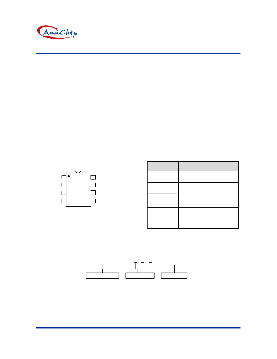
Connection Diagram
AP1121
7
5
4
3
2
1
6
GND
V
IN
V
OUT1
V
IN
(Top View)
8
V
OUT2
GND
GND
GND
Pin Descriptions
NAME
FUNCTION
GND Ground
3.3V(V
OUT1
)
2.5V/1.8V
(V
OUT2
)
The output of the regulator. A
minimum of 10uF capacitor
must be connected from this
pin to ground to insure
stability.
V
IN
The input pin of regulator.
Typically a large storage
capacitor is connected from
this pin to ground.
Ordering Information
AP 1121 X X X
Package
Vout
S : SOP-8L
Packing
Blank : Tube
A : Taping
A : CH1=3.3V
CH2=2.5V
B : CH1=3.3V
CH2=1.8V
AP1121
Dual 1A Low Dropout Positive Regulator
Anachip Corp.
www.anachip.com.tw
Rev. 0.0 Mar. 4, 2004
2/5
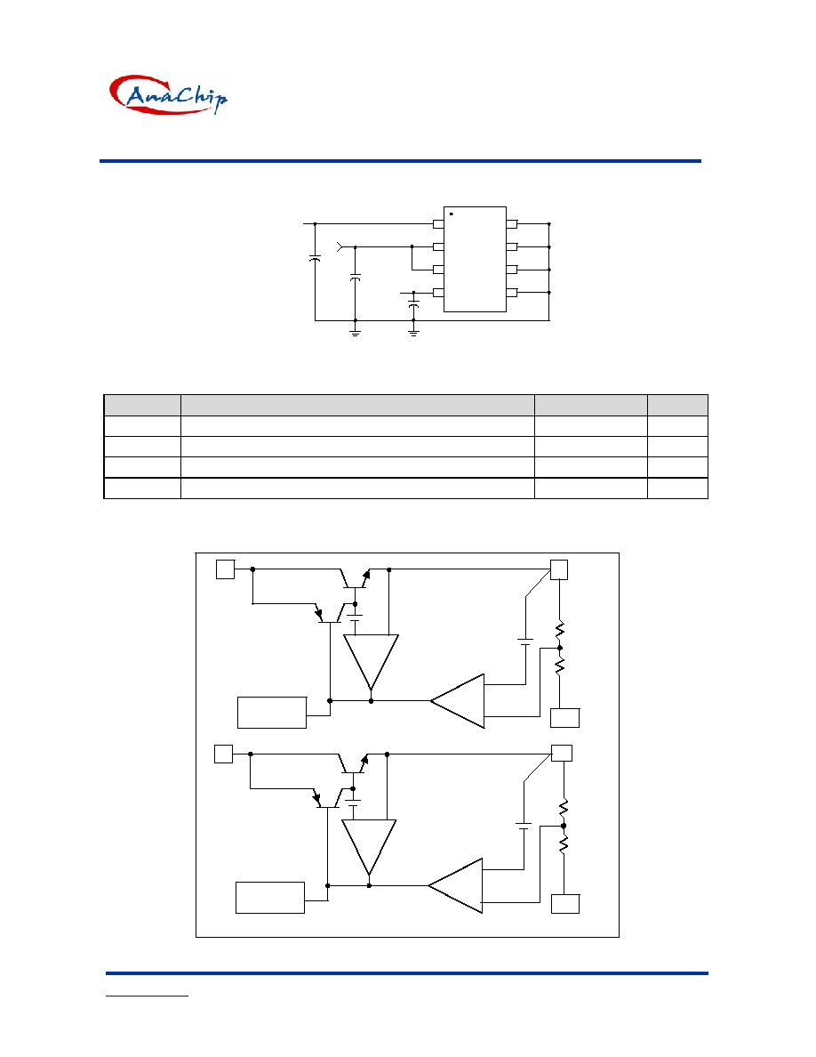
Typical Circuit
5V
3.3V/1A
C2
100uF
V
IN
V
OUT1
GND
V
IN
C1
100uF
C3
100uF
2.5V/1A
V
OUT2
GND
GND
GND
(3.3V/2.5V Dual output )
Absolute Maximum Ratings
Symbol
Parameter
Rating
Unit
V
IN
DC Supply Voltage
-0.3 to 18 V
V
P
D
Power Dissipation
Internally Limited
T
ST
Storage Temperature
-65 to +150
o
C
T
OP
Operating
Junction
Temperature
Range
0 to +150
o
C
Block Diagram
2
Thermal
Shutdown
1
V
OUT1
1.25V
+
+
CURRENT
LIMIT
V
IN
+
+
5/6
GND
3
Thermal
Shutdown
4
V
OUT2
1.25V
+
+
CURRENT
LIMIT
V
IN
+
+
7/8
GND

AP1121
Dual 1A Low Dropout Positive Regulator
Anachip Corp.
www.anachip.com.tw
Rev. 0.0 Mar. 4, 2004
3/6
Electrical Characteristics
(Under Operating Conditions)
PARAMETER
CONDITIONS
MIN
TYP
MAX
UNIT
AP1121_ - V
OUT1
I
OUT
= 10mA, T
J
= 25
o
C,
4.8VV
IN
12V
3.235
3.300 3.365 V
AP1121A - V
OUT2
I
OUT
= 10mA, T
J
= 25
o
C,
4VV
IN
12V
2.450
2.500 2.550 V
Output Voltage
AP1121B - V
OUT2
I
OUT
= 10mA, T
J
= 25
o
C,
4VV
IN
12V
1.764
1.800 1.836 V
Line Regulation
I
O
=10mA,V
OUT
+1.5V<V
IN
<12V, T
J
=25
o
C
0.2
%
AP1121 series
V
OUT1
V
IN
= 5V, 0I
OUT
1A,
T
J
=25
o
C (Note 1,2)
26 33
mV
Load Regulation
AP1121 series
V
OUT2
V
IN
=4V, 0mA<Io<1A,
T
J
=25
o
C (Note 1,2)
20 25
mV
Dropout Voltage
(V
IN
-V
OUT
)
I
OUT
= 1A,
V
OUT
=0.1%V
OUT
1.3
1.4 V
Current Limit
(V
IN
-V
OUT
) = 5V
1. 1
A
Minimum Load Current 0
o
CTj125
o
C (Note 3)
5 10
mA
Thermal Regulation
T
A
=25
o
C, 30ms pulse
0.008
0.04
%/W
Ripple Rejection
F=120Hz,C
OUT
=25uF Tantalum, I
OUT
=1A
60
70
dB
Temperature Stability
I
O
=10mA
0.5
%
JA
Thermal Resistance
Junction-to-Ambient
(No heat sink; No air
flow)
SOP8: Control Circuitry/Power Transistor
(Note4)
CH1 or CH2 only
CH1 & CH2 and PD1=PD2
50
45
O
C/W
JC
Thermal Resistance
Junction-to-Case
SOP8: Control Circuitry/Power Transistor
(Note 4)
CH1 or CH2 only
CH1 & CH2 and PD1=PD2
20
12
O
C/W
Note1: See thermal regulation specifications for changes in output voltage due to heating effects. Line and load regulation are
measured at a constant junction temperature by low duty cycle pulse testing. Load regulation is measured at the output lead =
1/18" from the package.
Note2: Line and load regulation are guaranteed up to the maximum power dissipation of 15W. Power dissipation is determined by the
input/output differentially and the output current. Guaranteed maximum power dissipation will not be available over the full
input/output range.
Note3: Quiescent current is defined as the minimum output current that requires maintaining regulation. At 12V input/output differential
the device is guaranteed to regulate if the output current is greater than 10mA.
Note4: Vout1 and Vout2 are connected to the PCB cupper area 5.5mm*5.5mm separately. If you need large PD or lower Tc & Tj,
please connect to the large cupper area >> 5.5mm*5.5mm (like 10mm*10mm).
AP1121
Dual 1A Low Dropout Positive Regulator
Anachip Corp.
www.anachip.com.tw
Rev. 0.0 Mar. 4, 2004
4/5
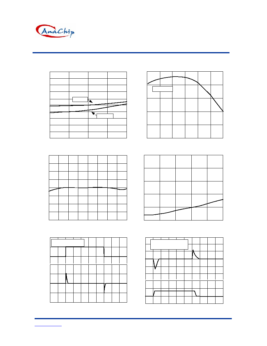
Typical Performance Characteristics
Temperature (
o
C)
Percent Change in Output Voltage vs Temperature
O
u
tput Vo
lta
ge Change
(%)
-50
-25
0
25
50
75
100
125
150
- 2
-1.5
- 1
-0.5
0
0. 5
1
1.5
2
Input Voltage (V)
Line Regulation
Outp
ut Voltage D
e
v
i
a
t
io
n
(%
)
0
0.2
0.4
0.6
0.8
1
2
4
6
8
10
12
TIME (us)
Line Transient Response
O
u
tput
V
o
l
t
age Dev
i
ati
o
n (m
V
)
I
n
put
V
o
lt
age (V)
-40
-20
0
20
40
5.5
6.5
7.5
Cin=1uF
Cout=10uF Tantalum
0
20
40
60
80
100 120 140 160 180 200
TIME (us)
Load Transient Response
Load Current
(A
)
Out
p
ut
V
o
lt
age Dev
i
at
i
o
n (m
V
)
0
10
20
30
40
50
60
70
80
90 100
-1
0
1
2
-20
-10
0
10
20
30
C in = 1uF
C out = 10 uF Tantalum
Preload = 100mA
Output Current (mA)
Dropout Voltage vs Output Current
D
r
opou
t Voltage (V)
0
0. 2
0. 4
0. 6
0. 8
1. 0
1. 2
1. 4
1. 6
1. 8
2. 0
0
200
400
600
800
Tj = 125
o
C
Tj = 25
o
C
Temperature (
o
C)
Load Regulation vs Temperature
O
u
tput Vo
lta
ge Dev
i
ation
(%)
-25
0
25
50
75
100
125
- 1
-0.80
-0.40
-0.20
0
0.20
I load=800mA

AP1121
Dual 1A Low Dropout Positive Regulator
Anachip Corp.
www.anachip.com.tw
Rev. 0.0 Mar. 4, 2004
5/5
Marking Information
SOP-8L
( Top View )
Logo
A : 3.3V/2.5V version
B : 3.3V/1.8V version
ID code: internal
Year: "01" =2001
"02" =2002
Xth week: 01~52
~
1
8
5
AC
AP1121 X
YY WW X
4
Package Information
VIEW "A"
L
C
VIEW "A"
H
E
A
A2
A1
B
e
D
7 (4X)
0.015x45
7 (4X)
y
Dimensions In Millimeters
Dimensions In Inches
Symbol
Min.
Nom.
Max.
Min.
Nom.
Max.
A 1.40 1.60 1.75
0.055
0.063
0.069
A1 0.10 - 0.25 0.040 - 0.100
A2 1.30 1.45 1.50 0.051
0.057
0.059
B 0.33 0.41 0.51
0.013
0.016
0.020
C 0.19 0.20 0.25
0.0075
0.008
0.010
D 4.80 5.05 5.30 0.189
0.199
0.209
E 3.70 3.90 4.10
0.146
0.154
0.161
e - 1.27 - -
0.050
-
H 5.79 5.99 6.20 0.228
0.236
0.244
L 0.38 0.71 1.27
0.015
0.028
0.050
y - - 0.10 - -
0.004
0
O
- 8
O
0
O
- 8
O