
1 04-02-051B
PA7540 PEEL ArrayTM
Programmable Electrically Erasable Logic Array
Most Powerful 24-pin PLD Available
- 20 I/Os, 2 inputs/clocks, 40 registers/latches
- 40 logic cell output functions
- PLA structure with true product-term sharing
- Logic functions and registers can be I/O-buried
Ideal for Combinatorial, Synchronous and
Asynchronous Logic Applications
- Integration of multiple PLDs and random logic
- Buried counters, complex state-machines
- Comparators, decoders, multiplexers and other wide-
gate functions
High-Speed Commercial and Industrial Versions
- As fast as 10ns/15ns (tpdi/tpdx), 71.4MHz (f
MAX
)
- Industrial grade available for 4.5 to 5.5V V
CC
and
-40 to +85 �C temperatures
CMOS Electrically Erasable Technology
- Reprogrammable in 24-pin DIP, SOIC and
28-pin
PLCC
packages
- Optional JN package for 22V10 power/ground
compatibility
Flexible Logic Cell
- 2 output functions per logic cell
- D,T and JK registers with special features
- Independent or global clocks, resets, presets,
clock polarity and output enables
- Sum-of-products logic for output enables
Development and Programmer Support
- Anachip's WinPLACE Development Software
- Fitters for ABEL, CUPL and other software
- Programming support by popular third-party
programmers
General Description
The PA7540 is a member of the Programmable Electrically
Erasable Logic (PEELTM) Array family based on ICT's
CMOS EEPROM technology. PEELTM Arrays free
designers from the limitations of ordinary PLDs by
providing the architectural flexibility and speed needed for
today's programmable logic designs. The PA7540 is by far
the most powerful 24-pin PLD available today with 20 I/O
pins, 2 input/global-clocks and 40 registers/latches (20
buried logic cells and 20 I/O registers/latches). Its logic
array implements 84 sum-of-products logic functions. The
PA7540's logic and I/O cells (LCCs, IOCs) are extremely
flexible offering two output functions per cell (a total of 40
for all 20 logic cells). Logic cells are configurable as D, T,
and JK registers with independent or global clocks, resets,
presets, clock polarity, and other features, making the
PA7540 suitable for a variety of combinatorial,
synchronous and asynchronous logic applications. With pin
compatibility and super-set functionality to most 24-pin
PLDs, (22V10, EP610/630, GAL6002), the PA7540 can
implement designs that exceed the architectures of such
devices. The PA7540 supports speeds as fast as
10ns/15ns (tpdi/tpdx) and 71.46MHz (f
MAX
) at moderate
power consumption 80mA (55mA typical). Packaging
includes 24-pin DIP, SOIC and 28-pin PLCC (see Figure
1). Anachip and popular third-party development tool
manufacturers provide development and programming
support for the PA7540.
Figure 1. Pin Configuration
DIP
I/CLK1
1
I/O
2
I/O
3
I/O
4
I/O
5
I/O
6
I/O
7
I/O
8
I/O
9
I/O
10
I/O
11
G ND
12
VCC
24
I/O
23
I/O
22
I/O
21
I/O
20
I/O
19
I/O
18
I/O
17
I/O
16
I/O
15
I/O
14
I/CLK2
13
1
I/CLK1
2
I/O
3
I/O
4
I/O
5
I/O
6
I/O
7
I/O
8
I/O
9
I/O
10
I/O
11
I/O
12
G ND
24
VCC
23
I/O
22
I/O
21
I/O
20
I/O
19
I/O
18
I/O
17
I/O
16
I/O
15
I/O
14
I/O
13
I/CLK2
SO IC
PLCC-JN
08-14-001B
12
I/O
13
I/O
14
GN
D
15
NC
16
I/C
L
K
2
17
I/O
18
I/O
25
I/O
24
I/O
23
I/O
22
NC
21
I/O
20
I/O
19
I/O
4
I/O
3
I/O
2
I/C
L
K
1
1
NC
28
VC
C
27
I/O
26
I/O
5
I/O
6
I/O
7
I/O
8
NC
9
I/O
10
I/O
11
I/O
5
I/O
6
I/O
7
I/O
8
NC
9
I/O
10
I/O
11
I/O
12
I/O
13
I/O
14
GN
D
15
GN
D
16
I/C
L
K
2
17
I/O
18
I/O
4
I/O
3
I/O
2
I/C
L
K
1
1
VC
C
28
VC
C
27
I/O
26
I/O
PLCC-J
25
I/O
24
I/O
23
I/O
22
NC
21
I/O
20
I/O
19
I/O
Figure 2. Block Diagram
PA7540
I/O
I/O
I/O
I/O
I/O
I/O
I/O
I/O
VC C
I/CLK 2
G ND
I/CLK 1
I/O
I/O
I/O
I/O
I/O
I/O
G lobal C ells
I/O C ells
I/O
I/O
I/O
I/O
I/O
I/O
Logic Control C ells
2 Input/
Global Clock Pins
Global
Cells
2
I/O
Cells
(IOC)
Logic
Control
Cells
(LCC)
20
20
20
20
A
B
C
D
84 (42X2)
Array Inputs
true and
com plem ent
Buried
logic
4 sum term s
4 product term s
for Global Cells
20 Logic Control Cells
2 output functions per cell
(40 total output functions possible)
Logic functions
to I/O cells
20 I/O Pins
80 sum term s
(four per LCC)
Logic
Array
08-14-002A
2 04-02-051B
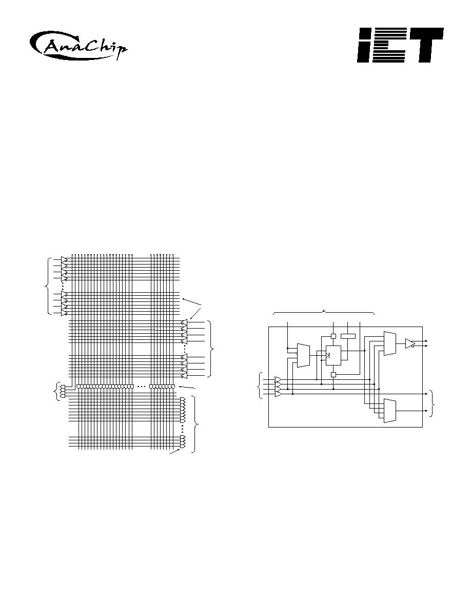
Inside the Logic Array
The heart of the PEELTM Array architecture is based on a
logic array structure similar to that of a PLA (programmable
AND, programmable OR). The logic array implements all
logic functions and provides interconnection and control of
the cells. In the PA7540 PEELTM Array, 42 inputs are
available into the array from the I/O cells and input/global-
clock pins.
All inputs provide both true and complement signals, which
can be programmed to any product term in the array. The
PA7540 PEELTM Arrays contains 84 product terms. All
product terms (with the exception of certain ones fed to the
global cells) can be programmably connected to any of the
sum-terms of the logic control cells (four sum-terms per
logic control cell). Product-terms and sum-terms are also
routed to the global cells for control purposes. Figure 3
shows a detailed view of the logic array structure.
From
IO C ells
(IO C) and
I/CLKs
From
Logic
Control
Cells
(LCC)
T o
G lobal
Cells
42 Array Inputs
84 Product Term s
T o
Logic C ontrol
Cells
(LCC)
84 Sum Term s
PA7540 Logic Array
08-14-003A
Figure 3 PA7540 Logic Array
True Product-Term Sharing
The PEELTM logic array provides several advantages over
common PLD logic arrays. First, it allows for true product-
term sharing, not simply product-term steering, as
commonly found in other CPLDs. Product term sharing
ensures that product-terms are used where they are
needed and not left unutilized or duplicated. Secondly, the
sum-of-products functions provided to the logic cells can be
used for clocks, resets, presets and output enables instead of
just simple product-term control.
The PEELTM logic array can also implement logic functions
with many product terms within a single-level delay. For
example a 16-bit comparator needs 32 shared product terms
to implement 16 exclusive-OR functions. The PEELTM logic
array easily handles this in a single level delay. Other
PLDs/CPLDs either run out of product-terms or require
expanders or additional logic levels that often slow
performance and skew timing.
Logic Control Cell (LCC)
Logic Control Cells (LCC) are used to allocate and control the
logic functions created in the logic array. Each LCC has four
primary inputs and three outputs. The inputs to each LCC are
complete sum-of-product logic functions from the array, which
can be used to implement combinatorial and sequential logic
functions, and to control LCC registers and I/O cell output
enables.
A
B
C
D
REG
D ,T,J
K
R
P
Q
MUX
System C lock
Preset
Reset
O n/O ff
RegType
From G lobal C ell
MUX
MUX
To
Array
To
I/O
Cell
From
Array
08-14-004A
Figure 4. Logic Control Cell Block Diagram
As shown in Figure 4, the LCC is made up of three signal
routing multiplexers and a versatile register with synchronous
or asynchronous D, T, or JK registers (clocked-SR registers,
which are a subset of JK, are also possible). See Figure 5.
EEPROM memory cells are used for programming the
desired configuration. Four sum-of-product logic functions
(SUM terms A, B, C and D) are fed into each LCC from the
logic array. Each SUM term can be selectively used for
multiple functions as listed below.

3 04-02-051B
Sum-A = D, T, J or Sum-A
Sum-B = Preset, K or Sum-B
Sum-C = Reset, Clock, Sum-C
Sum-D = Clock, Output Enable
D
R
P
Q
D R eg ister
Q = D after clocked
Best for storage, simple counters,
shifters and state machines with
few hold (loop) conditions.
T
R
P
Q
T R eg ister
Q toggles when T = 1
Q holds when T = 0
Best for wide binary counters (saves
product terms) and state machines
with many hold (loop) conditions.
JK R eg ister
Q toggles when J/K = 1/1
Q holds when J/K = 0/0
Q = 1 when J/K = 1/0
Q = 0 when J/K = 0/1
Combines features of both D and T
registers.
J
R
P
Q
K
08-14-005A
Figure 5. LCC Register Types
SUM-A can serve as the D, T, or J input of the register or a
combinatorial path. SUM-B can serve as the K input, or the
preset to the register, or a combinatorial path. SUM-C can
be the clock, the reset to the register, or a combinatorial
path. SUM-D can be the clock to the register or the output
enable for the connected I/O cell. Note that the sums
controlling clocks, resets, presets and output enables are
complete sum-of-product functions, not just product terms
as with most other PLDs. This also means that any input or
I/O pin can be used as a clock or other control function.
Several signals from the global cell are provided primarily
for synchronous (global) register control. The global cell
signals are routed to all LCCs. These signals include a
high-speed clock of positive or negative polarity, global
preset and reset, and a special register-type control that
selectively allows dynamic switching of register type. This
last feature is especially useful for saving product terms
when implementing loadable counters and state machines
by dynamically switching from D-type registers to load and
T-type registers to count (see Figure 10).
Multiple Outputs Per Logic Cell
An important feature of the logic control cell is its capability
to have multiple output functions per cell, each operating
independently. As shown in Figure 4, two of the three
outputs can select the Q output from the register or the
Sum A, B or C combinatorial paths. Thus, one LCC output
can be registered, one output can be combinatorial and the
third, an output enable. The multi-function PEELTM Array logic
cells are equivalent to two or three macrocells of other PLDs,
which have only one output per cell. They also allow registers
to be truly buried from I/O pins without limiting them to input-
only (see Figure 8 ).
7540 /O Cell (IOC)
MUX
From
Logic
Control
Cell
A,B,C
or
Q
MUX
1 0
D
I/O Pin
MUX
To
Array
REG/
Latch
Q
I/O Cell Clock
From Global Cell
Input
08-14-006A
Figure 6. I/O Cell Block Diagram
IO C R eg ister
Q = D after rising edge of clock
holds until next rising edge
IO C L atch
Q = L when clock is high
holds value when clock is low
L
Q
D
Q
08-14-007A
Figure 7. IOC Register Configurations
I/O Cell (IOC)
All PEELTM Arrays have I/O cells (IOC) as shown above in
Figure 6. Inputs to the IOCs can be fed from any of the LCCs
in the array. Each IOC consists of routing and control
multiplexers, an input register/transparent latch, a three-state
buffer and an output polarity control. The register/ latch can
be clocked from a variety of sources determined by the global
cell. It can also be bypassed for a non-registered input. The
combination of LCC and IOC allows for multiple buried
registers and logic paths. (See Figure 8).

4 04-02-051B
I/O with
independent
output enable
I/O
Q D
Input with optional
register/latch
A
B
C
D
1
2
O E
D Q
08-14-008A
Figure 8. LCC & IOC With Two Outputs
Global Cells
The global cells, shown in Figure 9, are used to direct
global clock signals and/or control terms to the LCCs and
IOCs. The global cells allow a clock to be selected from the
CLK1 pin, CLK2 pin, or a product term from the logic array
(PCLK). They also provide polarity control for IOC clocks
enabling rising or falling clock edges for input
registers/latches. Note that each individual LCC clock has
its own polarity control. The global cell includes sum-of-
products control terms for global reset and preset, and a
fast product term control for LCC register-type, used to
save product terms for loadable counters and state
machines (see Figure 10). The PA7540 provides two
global cells that divides the LCC and IOCs into two groups,
A and B. Half of the LCCs and IOCs use global cell A, half
use global cell B. This means, for instance, two high-speed
global clocks can be used among the LCCs.
Global Cell: LCC & IOC
MUX
MUX
CLK1
CLK2
PCLK
Reg-Type
Preset
Reset
LCC Resets
LCC Presets
LCC Reg-Type
IOC Clocks
LCC Clocks
Group A & B
08-14-009A
Figure 9. Global Cells
R e g ister T yp e C hang e F eature
G lobal Cell can dynamically change user-
selected LCC registers from D to T or from D
to JK. This saves product terms for loadable
counters or state machines. Use as D register
to load, use as T or JK to count. Timing allows
dynamic operation.
T
R
P
Q
D
R
P
Q
Reg-T ype from Global Cell
E x am p le:
Product terms for 10 bit loadable binary counter
D uses 57 product terms (47 count, 10 load)
T uses 30 product terms (10 count, 20 load)
D/T uses 20 product terms (10 count, 10 load)
08-14-010A
Figure 10. Register Type Change Feature
PEELTM Array Development Support
Development support for PEELTM Arrays is provided by
Anachip and manufacturers of popular development tools.
Anachip offers the powerful WinPLACE Development
Software (free to qualified PLD designers).
The PLACE software includes an architectural editor, logic
compiler, waveform simulator, documentation utility and a
programmer interface. The PLACE editor graphically
illustrates and controls the PEELTM Array's architecture,
making the overall design easy to understand, while
allowing the effectiveness of boolean logic equations, state
machine design and truth table entry. The PLACE compiler
performs logic transformation and reduction, making it
possible to specify equations in almost any fashion and fit
the most logic possible in every design. PLACE also
provides a multi-level logic simulator allowing external and
internal signals to be simulated and analyzed via a
waveform display.(See Figures 10a-c)
PEELTM Array development is also supported by popular
development tools, such as ABEL via Anachip's PEELTM
Array fitters. A special smart translator utility adds the
capability to directly convert JEDEC files for other devices
into equivalent JEDEC files for pin-compatible PEELTM
Arrays.
Programming
PEELTM Arrays are EE-reprogrammable in all package
types, plastic-DIP, PLCC and SOIC. This makes them an
ideal development vehicle for the lab. EE -
reprogrammability is also useful for production, allowing
unexpected changes to be made quickly and without

5 04-02-051B
waste. Programming of PEELTM Arrays is supported by
many popular third party programmers.
Design Security and Signature Word
The PEELTM Arrays provide a special EEPROM security bit
that prevents unauthorized reading or copying of designs.
Once set, the programmed bits of the PEELTM Arrays
cannot be accessed until the entire chip has been
electrically erased. Another programming feature,
signature word, allows a user-definable code to be
programmed into the PEELTM Array. The code can be read
back even after the security bit has been set. The signature
word can be used to identify the pattern programmed in the
device or to record the design revision.
Figure 11 - WinPLACE Architectural Editor for
PA7540
Figure 12 - WinPLACE LCC and IOC screen
Figure 13 - WinPLACE waveform and
simulator screen