
General Description
The AAT4280A SmartSwitchTM is a member of
AnalogicTech's Application Specific Power MOS-
FETTM (ASPMTM) product family. The AAT4280A is
a P-channel MOSFET power switch designed for
high-side load-switching applications. The device
has a typical R
DS(ON)
of 80m
, allowing increased
load switch power handling capacity and is avail-
able in three different versions with flexible turn-on
and turn-off characteristics -- from very fast to slew
rate limited. The standard AAT4280A (-1) version
has a slew rate limited turn-on load switch and is
functionally compatible with the AAT4250 device,
while offering superior R
DS(ON)
characteristics. The
AAT4280A (-2) version features fast load switch
turn-on capabilities, typically less than 500ns turn-
on and 3Ķs turn-off times. The AAT4280A (-3) vari-
ation offers a shutdown load discharge circuit to
rapidly turn off a load circuit when the switch is dis-
abled. All AAT4280A load switch versions operate
with an input voltage ranging from 1.5V to 5.5V,
making them ideal for both 3V and 5V systems.
Input logic levels are TTL and 2.5V to 5V CMOS
compatible. The quiescent supply current is very
low, typically 25nA.
The AAT4280A is available in a 6-pin SOT23 or an
8-pin SC70JW package and is specified over the
-40įC to 85įC temperature range.
Features
∑
1.5V to 5.5V Input Voltage Range
∑
Very Low R
DS(ON)
, Typically 80m
(5V)
∑
Slew Rate Limited Turn-On Time Options
∑
1ms
∑
0.5Ķs
∑
100Ķs
∑
Fast Shutdown Load Discharge Option
∑
Low Quiescent Current
∑
25nA (typ)
∑
TTL/CMOS Input Logic Level
∑
Temperature Range: -40ļC to 85įC
∑
4kV ESD Rating
∑
6-Pin SOT23 or 8-Pin SC70JW Package
Applications
∑
Cellular Telephones
∑
Digital Still Cameras
∑
Hot Swap Supplies
∑
Notebook Computers
∑
Personal Communication Devices
∑
Personal Digital Assistants (PDAs)
AAT4280A
Slew Rate Controlled Load Switch
Typical Application
AAT4280A
C
OUT
0.1
Ķ
F
C
IN
1
Ķ
F
OUT
IN
GND
V
OUT
GND
GND
V
IN
ON/OFF
GND
IN
ON
4280A.2004.11.1.0
1
SmartSwitch
TM

AAT4280A
Slew Rate Controlled Load Switch
2
4280A.2004.11.1.0
Pin Descriptions
Pin Configuration
SOT23-6
(Top View)
SC70JW-8
(Top View)
Selector Guide
Slew Rate
Active
Part Number
(typ)
Pull Down
Enable
AAT4280A-1
1mS
Active High
AAT4280A-2
0.5ĶS
Active High
AAT4280A-3
100ĶS
Active High
OUT
ON/OFF
GND
IN
IN
IN
IN
IN
1
2
3
4
5
6
7
8
GND
IN
GND
IN
ON/OFF
OUT
1
2
3
4
5
6
Pin #
SOT23-6
SC70JW
Symbol
Function
1
2
OUT
The pin is the P-channel MOSFET drain connection.
Bypass to ground through a 0.1uF capacitor.
2, 5
4
GND
Ground connection.
3
3
ON/OFF
Enable input.
4, 6
1, 5, 6, 7, 8
IN
The pin is the input to the P-channel MOSFET source.
Bypass to ground through a 1.0uF capacitor.

AAT4280A
Slew Rate Controlled Load Switch
4280A.2004.11.1.0
3
Absolute Maximum Ratings
(T
A
=25įC unless otherwise noted)
Note: Stresses above those listed in Absolute Maximum Ratings may cause permanent damage to the device. Functional operation at con-
ditions other than the operating conditions specified is not implied. Only one Absolute Maximum Rating should be applied at any one time.
Note 1: Human body model is a 100pF capacitor discharged through a 1.5k
resistor into each pin.
Thermal Characteristics
Note 2: Mounted on an AAT4280A demo board in still 25ļC air.
Value
Symbol
Description
SOT23-6
SC70JW-8
Units
JA
Thermal Resistance (SOT23-6 or SC70JW-8)
2
120
140
įC/W
P
D
Power Dissipation (SOT23-6 or SC70JW-8)
2
833
714
mW
Symbol
Description
Value
Units
V
IN
IN to GND
-0.3 to 6
V
V
ON
ON/OFF to GND
-0.3 to 6
V
V
OUT
OUT to GND
-0.3 to V
IN
+0.3
V
I
MAX
Maximum Continuous Switch Current
2.3
A
I
DM
Maximum Pulsed Current
IN
2.5V
6
A
IN < 2.5V
3
A
T
J
Operating Junction Temperature Range
-40 to 150
įC
T
LEAD
Maximum Soldering Temperature (at leads)
300
įC
V
ESD
ESD Rating
1
- HBM
4000
V
AAT4280A
Slew Rate Controlled Load Switch
4
4280A.2004.11.1.0
Electrical Characteristics
Unless otherwise noted, V
IN
= 5V, T
A
= 40 to 85įC; typical values are at TA=25įC.
Note 3: For V
IN
outside this range, consult typical ON/OFF threshold curve.
Symbol Description
Conditions
Min
Typ
Max Units
AAT4280A All Versions
V
IN
Operation Voltage
1.5
5.5
V
I
Q
Quiescent Current
ON/OFF= active
1
ĶA
I
Q
(off)
Off Supply Current
ON/OFF= inactive, OUT=open
1
ĶA
I
SD
(off)
Off Switch Current
ON/OFF= inactive, V
OUT
=0
1
ĶA
R
DS(on)
On-Resistance
V
IN
=5V, T
A
=25į C
80
120
m
V
IN
=4.2V, T
A
=25į C
85
130
V
IN
=3V, T
A
=25į C
100
150
V
IN
=1.8V, T
A
=25į C
160
250
TC
RDS
On-Resistance Temp -Co
2800
ppm/įC
V
IL
ON/OFF Input Logic Low Voltage
V
IN
=1.8V-5.5V
3
0.4
V
V
IN
=2.7V to 4.2V
2
V
IH
ON/OFF Input Logic High Voltage
V
IN
= 4.2V to 5.5V
2.4
V
V
IN
= 1.5V to 2.7V
1.4
I
SINK
ON/OFF Input Leakage
V
ON/OFF
= 5.5V
1
ĶA
AAT4280A-1
T
D(ON)
Output Turn-On Delay
V
IN
=5V, R
LOAD
=10
, T
A
=25į C
20
40
ĶS
T
ON
Output Turn-On Rise Time
V
IN
=5V, R
LOAD
=10
, T
A
=25į C
1000
1500
ĶS
T
D(OFF)
Output Turn-Off Delay Time
V
IN
=5V, R
LOAD
=10
, T
A
=25į C
4
10
ĶS
AAT4280A-2
T
D(ON)
Output Turn-On Delay
V
IN
=5V, R
LOAD
=10
, T
A
=25į C
0.5
2
ĶS
T
ON
Output Turn-On Rise Time
V
IN
=5V, R
LOAD
=10
, T
A
=25į C
0.5
1
ĶS
T
D(OFF)
Output Turn-Off Delay Time
V
IN
=5V, R
LOAD
=10
, T
A
=25į C
4
10
ĶS
AAT4280A-3
T
D(ON)
Output Turn-On Delay
V
IN
=5V, R
LOAD
=10
, T
A
=25į C
20
40
ĶS
T
ON
Output Turn-On Rise Time
V
IN
=5V, R
LOAD
=10
, T
A
=25į C
100
150
ĶS
T
D(OFF)
Output Turn_Off Delay Time
V
IN
=5V, R
LOAD
=10
, T
A
=25į C
4
10
ĶS
R
PD
Output pull-down resistance during OFF ON/OFF = inactive, T
A
=25į C
150
250
AAT4280A
Slew Rate Controlled Load Switch
4280A.2004.11.1.0
5
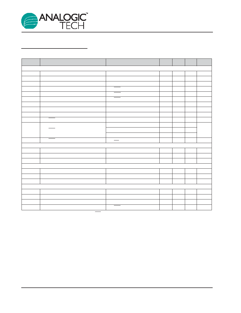
Typical Characteristics
Unless otherwise noted, V
IN
= 5V, T
A
= 25įC.
Off Switch Current vs. Temperature
0.001
0.010
0.100
1.000
-40
-20
0
20
40
60
80
100
Temperature (
į
C)
I
OFFSW
(
Ķ
A)
ON/OFF Threshold vs. V
IN
0.4
0.6
0.8
1.0
1.2
1.4
1.6
1.8
2.0
2.2
1.5
2.0
2.5
3.0
3.5
4.0
4.5
5.0
5.5
V
IN
(V)
ON/OFF Threshold (V)
V
IH
V
IL
R
DS(ON)
vs. Temperature
40
50
60
70
80
90
100
110
120
-40
-20
0
20
40
60
80
100
Temperature (
į
C)
R
DS(ON)
(m
)
V
IN
=5V
V
IN
=3V
R
DS(ON)
vs. V
IN
70
90
110
130
150
170
190
1.5
2.0
2.5
3.0
3.5
4.0
4.5
5.0
5.5
V
IN
(V)
R
DS(ON)
(m
)
2A
1A
500mA
100mA
Quiescent Current vs. Temperature
Temperature (
į
C)
I
Q
(nA)
0
10
20
30
40
50
-40
-20
0
20
40
60
80
100
AAT4280A
Slew Rate Controlled Load Switch
6
4280A.2004.11.1.0
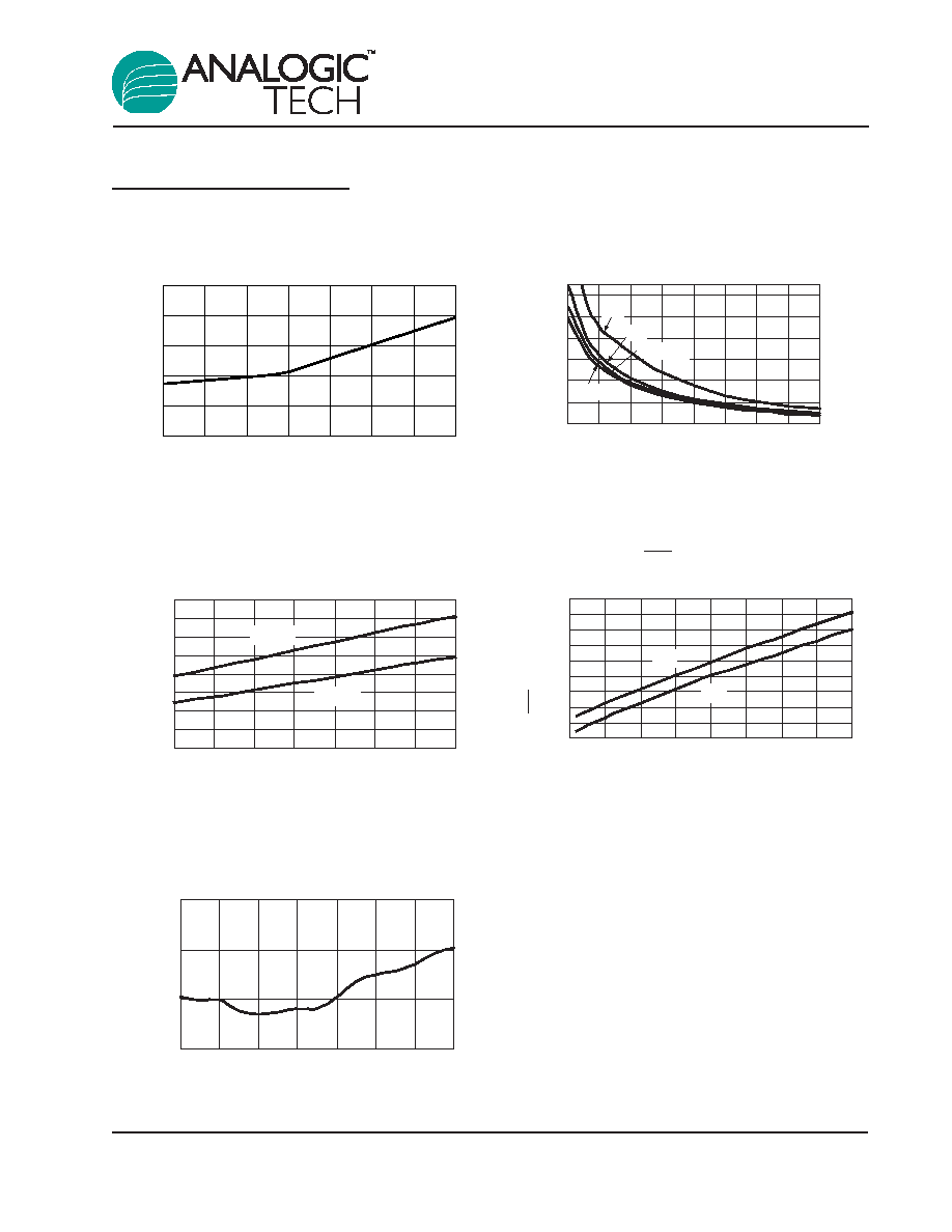
Typical Characteristics--4280A-1
Unless otherwise noted, V
IN
= 5V, T
A
= 25įC.
AAT4280A-1 Turn-Off
V
IN
=5V R
L
=10
Time (10
Ķ
s/div.)
ON/OFF (5V/div.)
V
OUT
(2V/div.)
I
IN
(200mA/div.)
AAT4280A-1 Turn-Off
V
IN
=3V R
L
=6
Time (10
Ķ
s/div)
ON/OFF (5V/div.)
V
OUT
(2V/div.)
I
IN
(200mA/div.)
AAT4280A-1 Turn-On
V
IN
=5V R
L
=10
Time (500
Ķ
s/div.)
ON/OFF (5V/div.)
V
OUT
(2V/div.)
I
IN
(200mA/div.)
AAT4280A-1 Turn-On
V
IN
=3V R
L
=6
Time (500
Ķ
s/div.)
ON/OFF (5V/div.)
V
OUT
(2V/div.)
I
IN
(200mA/div.)

AAT4280A
Slew Rate Controlled Load Switch
4280A.2004.11.1.0
7
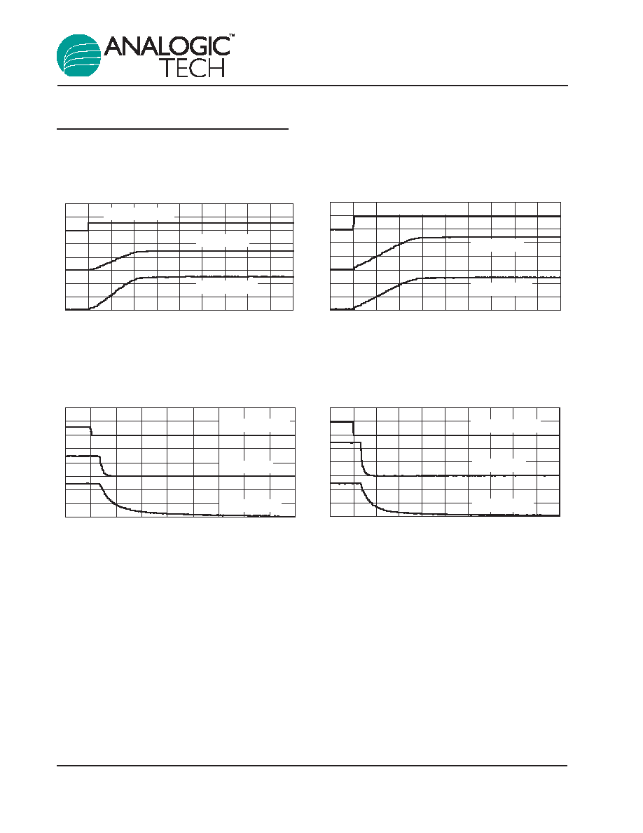
Typical Characteristics--4280A-2
Unless otherwise noted, V
IN
= 5V, T
A
= 25įC.
AAT4280A-2 Turn-Off
V
IN
=5V R
L
=10
Time (5
Ķ
s/div.)
ON/OFF (5V/div.)
V
OUT
(2V/div.)
I
IN
(200mA/div.)
AAT4280A-2 Turn-Off
V
IN
=3V R
L
=6
Time (5
Ķ
s/div.)
ON/OFF (5V/div.)
V
OUT
(2V/div.)
I
IN
(200mA/div.)
AAT4280A-2 Turn-On
V
IN
=5V R
L
=10
Time (5
Ķ
s/div.)
ON/OFF (5V/div.)
V
OUT
(2V/div.)
I
IN
(200mA/div.)
AAT4280A-2 Turn-On
V
IN
=3V R
L
=6
Time (5
Ķ
s/div.)
ON/OFF (5V/div.)
V
OUT
(2V/div.)
I
IN
(200mA/div.)

AAT4280A
Slew Rate Controlled Load Switch
8
4280A.2004.11.1.0
Typical Characteristics--4280A-3
Unless otherwise noted, V
IN
= 5V, T
A
= 25įC.
AAT4280A-3 Turn-Off
V
IN
=5V R
L
=10
Time (5
Ķ
s/div.)
ON/OFF (5V/div.)
V
OUT
(2V/div.)
I
IN
(200mA/div.)
AAT4280A-3 Turn-Off
V
IN
=3V R
L
=6
Time (5
Ķ
s/div.)
ON/OFF (5V/div.)
V
OUT
(2V/div.)
I
IN
(200mA/div.)
AAT4280A-3 Turn-On
V
IN
=5V R
L
=10
Time (50
Ķ
s/div.)
ON/OFF (5V/div.)
V
OUT
(2V/div.)
I
IN
(200mA/div.)
AAT4280A-3 Turn-On
V
IN
=3V R
L
=6
Time (50
Ķ
s/div.)
ON/OFF (5V/div.)
V
OUT
(2V/div.)
I
IN
(200mA/div.)

AAT4280A
Slew Rate Controlled Load Switch
4280A.2004.11.1.0
9
Functional Description
The AAT4280A is a family of flexible P-channel
MOSFET power switches designed for high-side
load switching applications. There are three ver-
sions of the AAT4280A with different turn-on and
turn-off characteristics to choose from, depending
upon the specific requirements of an application.
The first version, AAT4280A-1, has a moderate
turn-on slew rate feature, which reduces in-rush
current when the MOSFET is turned on. This func-
tion allows the load switch to be implemented with
a small input capacitor, or no input capacitor at all.
During turn-on slewing, the current ramps linearly
until it reaches the level required for the output load
condition. The proprietary turn-on current control
method works by careful control and monitoring of
the MOSFET gate voltage. When the device is
switched ON, the gate voltage is quickly increased
to the threshold level of the MOSFET. Once at this
level, the current begins to slew as the gate voltage
is slowly increased until the MOSFET becomes
fully enhanced. Once it has reached this point, the
gate is quickly increased to the full input voltage
and R
DS(ON)
is minimized. The second version, the
AAT4280A-2, is a very fast switch intended for
high-speed switching applications. This version
has no turn-on slew rate control and no special out-
put discharge features. The final switch version,
the AAT4280A-3, has the addition of a minimized
slew rate limited turn-on function and a shutdown
output discharge circuit to rapidly turn off a load
when the load switch is disabled through the
ON/OFF pin.
All versions of the AAT4280A operate with input
voltages ranging from 1.5V to 5.5V. All versions of
this device have extremely low operating current,
making them ideal for battery-powered applica-
tions. The ON/OFF control pin is TTL compatible
and will also function with 2.5V to 5V logic systems,
making the AAT4280A an ideal level shifting load-
switch.
Functional Block Diagram
Level
Shift
IN
ON/OFF
OUT
GND
Turn-On
Slew Rate
Control
*
*AAT4280A-3 only

AAT4280A
Slew Rate Controlled Load Switch
10
4280A.2004.11.1.0
Applications Information
Input Capacitor
Typically a 1ĶF or larger capacitor is recommend-
ed for C
IN
in most applications. A C
IN
capacitor is
not required for basic operation; however, C
IN
is
useful in preventing load transients from affecting
upstream circuits. C
IN
should be located as close
to the device V
IN
pin as practically possible.
Ceramic, tantalum, or aluminum electrolytic capac-
itors may be selected for C
IN
. There is no specific
capacitor ESR requirement for C
IN
; however, for
higher current operation, ceramic capacitors are
recommended for C
IN
due to their inherent capabil-
ity over tantalum capacitors to withstand input cur-
rent surges from low impedance sources, such as
batteries in portable devices.
Output Capacitor
For proper slew operation, a 0.1ĶF capacitor or
greater between V
OUT
and GND is recommended.
The output capacitor has no specific capacitor type
or ESR requirement. If desired, C
OUT
may be
increased without limit to accommodate any load
transient condition without adversely affecting the
device turn-on slew rate time.
Enable Function
The AAT4280A features an enable / disable func-
tion. This pin (ON/OFF) is compatible with both
TTL or CMOS logic.
Reverse Output-to-Input Voltage
Conditions and Protection
Under normal operating conditions, a parasitic
diode exists between the output and input of the
load switch. The input voltage should always
remain greater than the output load voltage main-
taining a reverse bias on the internal parasitic
diode. Conditions where V
OUT
might exceed V
IN
should be avoided since this would forward bias
the internal parasitic diode and allow excessive
current flow into the V
OUT
pin and possible damage
to the load switch.
In applications where there is a possibility of V
OUT
exceeding V
IN
for brief periods of time during normal
operation, the use of a larger value C
IN
capacitor is
highly recommended. A larger value of C
IN
with
respect to C
OUT
will effect a slower C
IN
decay rate
during shutdown, thus preventing V
OUT
from
exceeding V
IN
. In applications where there is a
greater danger of V
OUT
exceeding V
IN
for extended
periods of time, it is recommended to place a
Schottky diode from V
IN
to V
OUT
(connecting the
cathode to V
IN
and anode to V
OUT
). The Schottky
diode forward voltage should be less than 0.45V.
Thermal Considerations and
High Output Current Applications
The AAT4280A is designed to deliver a continuous
output load current. The limiting characteristic for
maximum safe operating output load current is
package power dissipation. In order to obtain high
operating currents, careful device layout and circuit
operating conditions need to be taken into account.
The following discussions will assume the load
switch is mounted on a printed circuit board utiliz-
ing the minimum recommended footprint, as stated
in the layout considerations section.
At any given ambient temperature (T
A
), the maxi-
mum package power dissipation can be deter-
mined by the following equation:
P
D(MAX)
= [T
J(MAX)
- T
A
] /
JA
Constants for the AAT4280A are maximum junction
temperature, T
J(MAX)
= 125įC, and package thermal
resistance,
JA
= 120įC/W. Worst case conditions
are calculated at the maximum operating tempera-
ture where T
A
= 85įC. Typical conditions are cal-
culated under normal ambient conditions where T
A
= 25įC. At T
A
= 85įC, P
D(MAX)
= 333mW. At T
A
=
25įC, P
D(MAX)
= 833mW.
The maximum continuous output current for the
AAT4280A is a function of the package power dissi-
pation and the R
DS
of the MOSFET at T
J(MAX)
. The
maximum R
DS
of the MOSFET at T
J(MAX)
is calcu-
lated by increasing the maximum room temperature
R
DS
by the R
DS
temperature coefficient. The tem-
perature coefficient (T
C
) is 2800ppm/įC. Therefore,
MAX R
DS
125įC = R
DS
25įC
◊
(1 + T
C
◊
T)
MAX R
DS
125įC = 120m
◊
(1 + 0.0028
◊
(125įC - 25įC)) = 154m

AAT4280A
Slew Rate Controlled Load Switch
4280A.2004.11.1.0
11
For maximum current, refer to the following equation:
I
OUT(MAX)
< ( P
D(MAX)
/ R
DS
)
1/2
For example, if V
IN
= 5V, R
DS(MAX)
=154m
and T
A
= 25įC, I
OUT(MAX)
= 2.3A. If the output load current
were to exceed 2.3A or if the ambient temperature
were to increase, the internal die temperature
would increase and the device would be damaged.
Higher peak currents can be obtained with the
AAT4280A. To accomplish this, the device thermal
resistance must be reduced by increasing the heat
sink area or by operating the load switch in a duty
cycle manner.
High Peak Output Current Applications
Some applications require the load switch to oper-
ate at a continuous nominal current level with short
duration, high-current peaks. The duty cycle for
both output current levels must be taken into
account. To do so, first calculate the power dissi-
pation at the nominal continuous current level, and
then add in the additional power dissipation due to
the short duration, high-current peak scaled by the
duty factor.
For example, a 4V system using an AAT4280A
operates at a continuous 100mA load current level
and has short 2A current peaks, as in a GSM appli-
cation. The current peak occurs for 576Ķs out of a
4.61ms period.
First, the current duty cycle is calculated:
% Peak Duty Cycle: X/100 = 576Ķs/4.61ms
% Peak Duty Cycle = 12.5%
The load current is 100mA for 87.5% of the 4.61ms
period and 2A for 12.5% of the period. Since the
Electrical Characteristics do not report R
DS(MAX)
for
4V operation, it must be calculated approximately
by consulting the chart of R
DS(ON)
vs. V
IN
. The R
DS
reported for 5V can be scaled by the ratio seen in
the chart to derive the R
DS
for a 4V V
IN
: 120m
◊
87m
/80m
= 130m
. De-rated for temperature:
130m
x (1 + .0028
◊
(125įC -25įC)) = 166m
.
The power dissipation for a 100mA load is calculat-
ed as follows:
P
D(MAX)
= I
OUT
2
◊
R
DS
P
D(100mA)
= (100mA)
2
◊
166m
P
D(100mA)
= 1.66mW
P
D(87.5%D/C)
= %DC
◊
P
D(100mA)
P
D(87.5%D/C)
= 0.875
◊
1.66mW
P
D(87.5%D/C)
= 1.45mW
The power dissipation for 100mA load at 87.5%
duty cycle is 1.45mW. Now the power dissipation
for the remaining 12.5% of the duty cycle at 2A is
calculated:
P
D(MAX)
= I
OUT
2
◊
R
DS
P
D(2A)
= (2A)
2
◊
166m
P
D(2A)
= 664mW
P
D(12.5%D/C)
= %DC
◊
P
D(2A)
P
D(12.5%D/C)
= 0.125
◊
664mW
P
D(12.5%D/C)
= 83mW
The power dissipation for 2A load at 12.5% duty
cycle is 83mW. Finally, the two power figures are
summed to determine the total true power dissipa-
tion under the varied load:
P
D(total)
= P
D(100mA)
+ P
D(2A)
P
D(total)
= 1.45mW + 83mW
P
D(total)
= 84.5mW
The maximum power dissipation for the AAT4280A
operating at an ambient temperature of 85įC is
333mW. The device in this example will have a
total power dissipation of 84.5mW. This is well
within the thermal limits for safe operation of the
device; in fact, at 85įC, the AAT4280A will handle
a 2A pulse for up to 50% duty cycle. At lower ambi-
ent temperatures, the duty cycle can be further
increased.

AAT4280A
Slew Rate Controlled Load Switch
12
4280A.2004.11.1.0
Figure 1: Evaluation board
Figure 2: Evaluation board
Figure 3: Evaluation board
top side silk screen layout /
component side layout
solder side layout
assembly drawing
Printed Circuit Board
Layout Recommendations
For proper thermal management and to take
advantage of the low R
DS(ON)
of the AAT4280A, a
few circuit board layout rules should be followed:
V
IN
and V
OUT
should be routed using wider than
normal traces, and GND should be connected to a
ground plane. To maximize package thermal dis-
pation and power handling capacity of the
AAT4280A SOT23-6 and SC70JW-8 packages, the
ground plane area connected to the ground pins
should be made as large as possible. For best per-
formance, C
IN
and C
OUT
should be placed close to
the package pins.
Evaluation Board Layout
The AAT4280A evaluation layout follows the print-
ed circuit board layout recommendations and can
be used for good applications layout. Refer to
Figures 1 through 3.
Note: Board layout shown is not to scale.
AAT4280A
Slew Rate Controlled Load Switch
4280A.2004.11.1.0
13
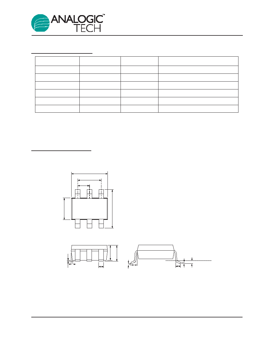
Ordering Information
Note: Sample stock is held for part numbers listed in BOLD.
Note 1: XYY = assembly and date code.
Package Information
SOT23-6
All dimensions in millimeters.
1.90 BSC
0.95 BSC
0.45
Ī
0.15
0.10 BSC
2.85
Ī
0.15
0.075
Ī
0.075
0.40
Ī
0.10
◊
6
1.575
Ī
0.125
1.20
Ī
0.25
1.10
Ī
0.20
2.80
Ī
0.20
4
į
Ī
4
į
10
į
Ī
5
į
0.15
Ī
0.07
GAUGE PLANE
0.60 REF
Device Option
Package
Marking
1
Part Number (Tape and Reel)
AAT4280A-1
SOT23-6
AAT4280AIGU-1-T1
AAT4280A-2
SOT23-6
AAT4280AIGU-2-T1
AAT4280A-3
SOT23-6
AAT4280AIGU-3-T1
AAT4280A-1
SC70JW-8
NDXYY
AAT4280AIJS-1-T1
AAT4280A-2
SC70JW-8
NEXYY
AAT4280AIJS-2-T1
AAT4280A-3
SC70JW-8
NFXYY
AAT4280AIJS-3-T1

SC70JW-8
All dimensions in millimeters.
0.225
Ī
0.075
0.45
Ī
0.10
0.05
Ī
0.05
2.10
Ī
0.30
2.00
Ī
0.20
7
į
Ī
3
į
4
į
Ī
4
į
1.75
Ī
0.10
0.85
Ī
0.15
0.15
Ī
0.05
1.10 MAX
0.100
2.20
Ī
0.20
0.048REF
0.50 BSC 0.50 BSC 0.50 BSC
AAT4280A
Slew Rate Controlled Load Switch
14
4280A.2004.11.1.0
Advanced Analogic Technologies, Inc.
830 E. Arques Avenue, Sunnyvale, CA 94085
Phone (408) 737-4600
Fax (408) 737-4611
AnalogicTech cannot assume responsibility for use of any circuitry other than circuitry entirely embodied in an AnalogicTech product. No circuit patent licenses, copyrights, mask work
rights, or other intellectual property rights are implied.
AnalogicTech reserves the right to make changes to their products or specifications or to discontinue any product or service without notice, and advise customers to obtain the latest
version of relevant information to verify, before placing orders, that information being relied on is current and complete. All products are sold subject to the terms and conditions of sale
supplied at the time of order acknowledgement, including those pertaining to warranty, patent infringement, and limitation of liability.
AnalogicTech warrants performance of its semiconductor products to the specifications applicable at the time of sale in accordance with AnalogicTech's standard warranty. Testing and
other quality control techniques are utilized to the extent AnalogicTech deems necessary to support this warranty. Specific testing of all parameters of each device is not necessarily
performed.