05/2003
ACA2404
750/870 MHz CATV
High Output Power Doubler Line Amplifier
ADVANCED PRODUCT INFORMATION - Rev 0.0
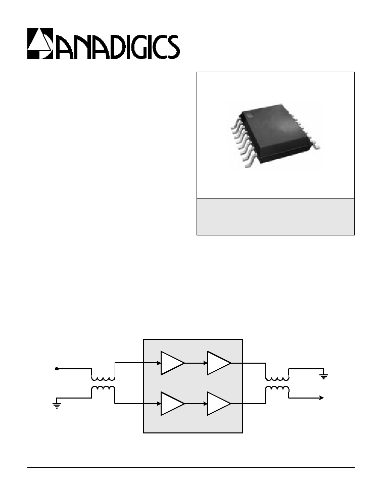
Figure 1: Hybrid Application Diagram
FEATURES
∑ 21.5 dB Gain
∑ Characterized at +58 dBmV Output
∑ Very Low Distortion
∑ Excellent 75
Input and Output Match
∑ Stable with High VSWR Load Conditions
∑ Monolithic Design for Consistent Performance
Part-to-Part
∑ Surface Mount Package Compatible with
Automatic Assembly
∑ Low Cost Alternative to Hybrids
∑ Meets Cenelec Standards
APPLICATIONS
∑ CATV Line Amplifiers, System Amplifiers,
Distribution Nodes
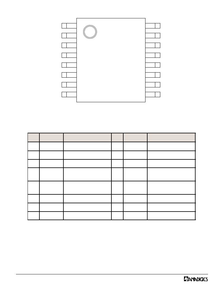
S7 Package
16 Pin Wide Body SOIC
with Heat Slug
PRODUCT DESCRIPTION
The ACA2404 is a highly linear, high output power,
monolithic GaAs RF amplifier that has been
developed to replace standard CATV hybrid
amplifiers, in new designs. Offered in a convenient
surface mount package, the MMIC consists of two
pairs of parallel amplifiers that are optimized for
exceptionally low distortion and noise figure. A hybrid
equivalent that provides flat gain response and
excellent input and output return loss over the 40 to
870 MHz CATV downstream band is formed when
one ACA2404 is cascaded between two appropriate
transmission line baluns.
RF Input
RF Output
2A
2B
1B
1A
ACA2404
2
ADVANCED PRODUCT INFORMATION - Rev 0.0
05/2003
ACA2404
Figure 2: Pin Out
Table 1: Pin Description
1
2
3
4
5
6
7
8
16
15
14
13
12
11
10
9
GND
GND
I
SET
2A
IN
GND
2B
IN
1B
IN
1A
IN
GND
GND
1B
OUT
2B
OUT
2A
OUT
1A
OUT
Bias 1A
Bias 1B
N
I
P
E
M
A
N
N
O
I
T
P
I
R
C
S
E
D
N
I
P
E
M
A
N
N
O
I
T
P
I
R
C
S
E
D
1
D
N
G
d
n
u
o
r
G
9
D
N
G
d
n
u
o
r
G
2
A
2
N
I
t
u
p
n
I
A
2
r
e
if
il
p
m
A
0
1
B
1
T
U
O
t
u
p
t
u
O
B
1
r
e
if
il
p
m
A
3
D
N
G
d
n
u
o
r
G
1
1
B
1
s
a
i
B
r
e
if
il
p
m
A
B
1
r
o
f
s
a
i
B
4
A
1
N
I
t
u
p
n
I
A
1
r
e
if
il
p
m
A
2
1
B
2
T
U
O
d
n
a
t
u
p
t
u
O
B
2
r
e
if
il
p
m
A
y
l
p
p
u
S
5
B
1
N
I
t
u
p
n
I
B
1
r
e
if
il
p
m
A
3
1
A
2
T
U
O
d
n
a
t
u
p
t
u
O
A
2
r
e
if
il
p
m
A
y
l
p
p
u
S
6
I
T
E
S
t
s
u
j
d
A
t
n
e
r
r
u
C
4
1
A
1
s
a
i
B
r
e
if
il
p
m
A
A
1
r
o
f
s
a
i
B
7
B
2
N
I
t
u
p
n
I
B
2
r
e
if
il
p
m
A
5
1
A
1
T
U
O
t
u
p
t
u
O
A
1
r
e
if
il
p
m
A
8
D
N
G
d
n
u
o
r
G
6
1
D
N
G
d
n
u
o
r
G

ADVANCED PRODUCT INFORMATION - Rev 0.0
05/2003
3
ACA2404
Table 2: Absolute Mimimum and Maximum Ratings
ELECTRICAL CHARACTERISTICS
Stresses in excess of the absolute ratings may cause permanent
damage. Functional operation is not implied under these conditions.
Exposure to absolute ratings for extended periods of time may
adversely affect reliability.
Table 3: Operating Ranges
Notes:
1. Pins 2, 4, 5 and 7 should be AC-coupled. No external DC bias should
be applied.
2. Pins 11 and 14 are bias feeds for input amplifiers 1A and 1B. No
external DC bias should be applied.
3. Pins 10 and 15 receive DC bias directly from pins 11 and 14. No other
external bias should be applied.
The device may be operated safely over these conditions; however, parametric
performance is guaranteed only over the conditions defined in the electrical
specifications.
R
E
T
E
M
A
R
A
P
N
I
M
X
A
M
T
I
N
U
)
3
1
,
2
1
s
n
i
p
(
y
l
p
p
u
S
0
8
2
+
C
D
V
)
6
n
i
p
(
t
s
u
j
d
A
t
n
e
r
r
u
C
0
4
+
C
D
V
)
5
,
4
s
n
i
p
(
s
t
u
p
n
I
t
a
r
e
w
o
P
F
R
-
5
7
+
V
m
B
d
e
r
u
t
a
r
e
p
m
e
T
e
g
a
r
o
t
S
5
6
-
0
5
1
+
C
∞
e
r
u
t
a
r
e
p
m
e
T
g
n
ir
e
d
l
o
S
-
0
6
2
+
C
∞
e
m
i
T
g
n
ir
e
d
l
o
S
-
0
.
5
c
e
S
R
E
T
E
M
A
R
A
P
N
I
M
P
Y
T
X
A
M
T
I
N
U
V
:
y
l
p
p
u
S
D
D
)
3
1
,
2
1
s
n
i
p
(
-
4
2
+
-
C
D
V
)
6
n
i
p
(
t
s
u
j
d
A
t
n
e
r
r
u
C
-
3
+
-
C
D
V
y
c
n
e
u
q
e
r
F
F
R
0
4
-
0
7
8
z
H
M
e
r
u
t
a
r
e
p
m
e
T
e
s
a
C
0
4
-
-
0
1
1
+
C
∞
4
ADVANCED PRODUCT INFORMATION - Rev 0.0
05/2003
ACA2404
Table 4: AC and DC Electrical Specifications
(T
A
= +25 ∞C, V
DD
= +24 VDC)
Notes:
(1) Measured with baluns on the input and output of the device.
(2) Parts measured with 77 channels, +58 dBmV power, 13.5 dB tilt at 870 MHz.
(3) Parts measured with 110 channels, +54 dBmV power, 13.5 dB tilt at 870 MHz.
4. All specifications as measured on Evaluation Board (see Figures 13 & 14).
R
E
T
E
M
A
R
A
P
N
I
M
P
Y
T
X
A
M
T
I
N
U
S
T
N
E
M
M
O
C
z
H
M
0
7
8
t
a
n
i
a
G
)
1
(
8
.
0
2
5
.
1
2
1
.
2
2
B
d
e
p
o
l
S
t
n
e
l
a
v
i
u
q
E
e
l
b
a
C
)
1
(
-
0
-
B
d
s
s
e
n
t
a
l
F
n
i
a
G
)
1
(
z
H
M
0
7
8
o
t
-
2
.
0
±
-
B
d
e
r
u
g
i
F
e
s
i
o
N
)
1
(
-
0
.
4
0
.
5
B
d
B
T
C
)
1
(
s
l
e
n
n
a
h
C
7
7
)
2
(
s
l
e
n
n
a
h
C
0
1
1
)
3
(
-
-
5
7
-
7
6
-
0
7
-
-
c
B
d
O
S
C
)
1
(
s
l
e
n
n
a
h
C
7
7
)
2
(
s
l
e
n
n
a
h
C
0
1
1
)
3
(
-
-
9
6
-
4
6
-
7
6
-
-
c
B
d
D
O
M
X
)
1
(
s
l
e
n
n
a
h
C
7
7
)
2
(
s
l
e
n
n
a
h
C
0
1
1
)
3
(
-
-
2
6
-
0
6
-
0
6
-
-
c
B
d
)
t
u
p
t
u
O
/t
u
p
n
I
(
s
s
o
L
n
r
u
t
e
R
)
1
(
8
1
2
2
-
B
d
5
7
m
e
t
s
y
s
t
n
e
r
r
u
C
y
l
p
p
u
S
5
8
4
0
0
5
5
1
5
A
m
e
c
n
a
t
s
i
s
e
R
l
a
m
r
e
h
T
-
7
.
2
3
.
3
W
/
C
∞

ADVANCED PRODUCT INFORMATION - Rev 0.0
05/2003
5
ACA2404
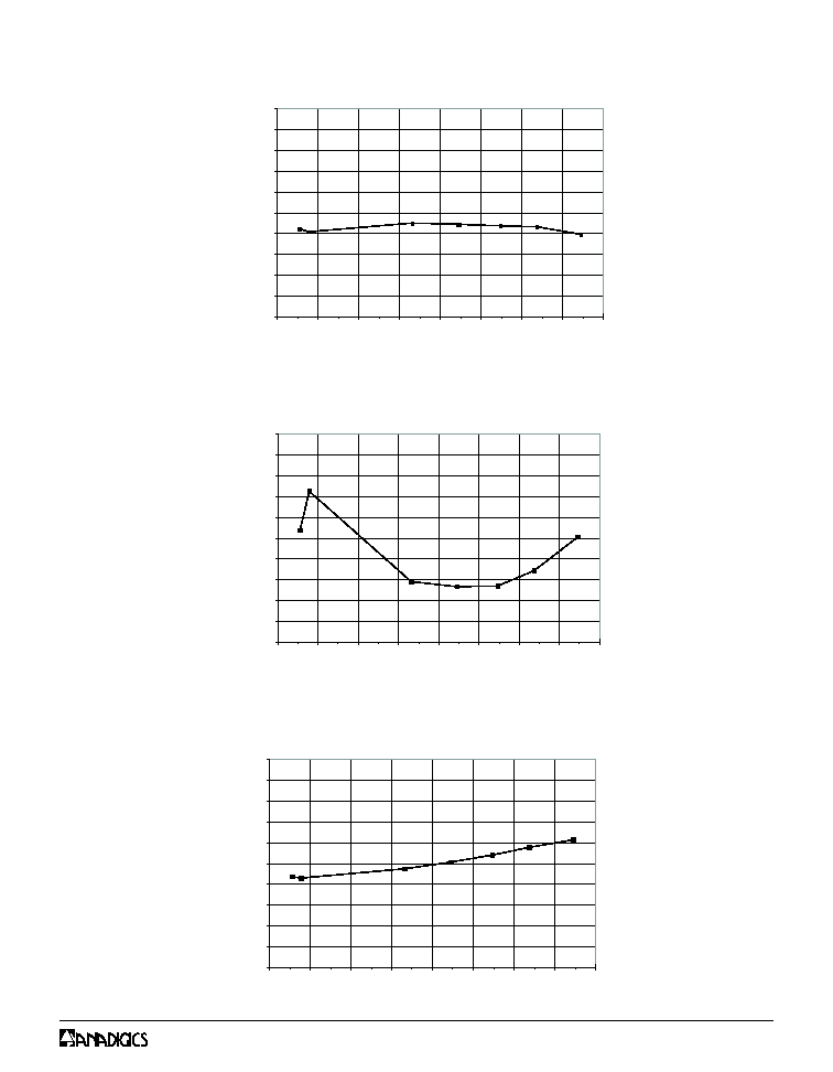
PERFORMANCE DATA
Figure 3: Noise Figure vs. Frequency
(T = +25 ∞C, V
= +24 V)
A
DD
2.0
2.5
3.0
3.5
4.0
4.5
5.0
0
100
200
300
400
500
600
700
800
900
1000
Frequency (MHz)
N
o
is
e
F
igu
r
e
(
dB
)
Figure 4: Gain (S21) vs. Frequency
(T = +25 ∞C, V
= +24 V, 75
system)
A
DD
W
19.0
19.5
20.0
20.5
21.0
21.5
22.0
22.5
23.0
23.5
24.0
0
100
200
300
400
500
600
700
800
900
1000
Frequency (MHz)
Ga
i
n
(
d
B
)

6
ADVANCED PRODUCT INFORMATION - Rev 0.0
05/2003
ACA2404
Figure 5: Input and Output Return Loss (S11 and S22) vs. Frequency
(T = +25 ∞C, V
= +24 V, 75
system)
A
DD
W
-50
-45
-40
-35
-30
-25
-20
-15
-10
-5
0
0
100
200
300
400
500
600
700
800
900
1000
Frequency (MHz)
R
e
tu
r
n
L
o
s
s
(d
B
)
S11
S22
Figure 6: Isolation (S12) vs. Frequency
(T = +25 ∞C, V
= +24 V, 75
system)
A
DD
W
-50
-45
-40
-35
-30
-25
-20
-15
-10
-5
0
0
100
200
300
400
500
600
700
800
900
1000
Frequency (MHz)
Is
ol
a
t
ion
(
dB
)
ADVANCED PRODUCT INFORMATION - Rev 0.0
05/2003
7
ACA2404
Figure 7: CTB vs. Frequency
(110 channels, +54 dBmV power, 13.5 dB tilt at 870 MHz)
-90
-85
-80
-75
-70
-65
-60
-55
-50
-45
-40
0
100
200
300
400
500
600
700
800
Frequency (MHz)
CT
B
(
d
B
c
)
Figure 8: CSO vs. Frequency
(110 channels, +54 dBmV power, 13.5 dB tilt at 870 MHz)
-100
-95
-90
-85
-80
-75
-70
-65
-60
-55
-50
0
100
200
300
400
500
600
700
800
Frequency (MHz)
CS
O
(
d
B
c
)
Figure 9: XMOD vs. Frequency
(110 channels, +54 dBmV power, 13.5 dB tilt at 870 MHz)
-90
-85
-80
-75
-70
-65
-60
-55
-50
-45
-40
0
100
200
300
400
500
600
700
800
Frequency (MHz)
XM
O
D
(d
B
c
)
8
ADVANCED PRODUCT INFORMATION - Rev 0.0
05/2003
ACA2404
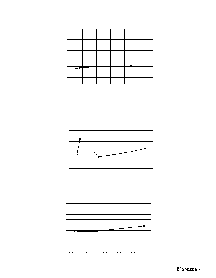
Figure 12: XMOD vs. Frequency
(77 channels, +58 dBmV power, 13.5 dB tilt at 870 MHz)
-90
-85
-80
-75
-70
-65
-60
-55
-50
-45
-40
0
100
200
300
400
500
600
Frequency (MHz)
XM
O
D
(d
B
c
)
Figure 11: CSO vs. Frequency
(77 channels, +58 dBmV power, 13.5 dB tilt at 870 MHz)
-100
-95
-90
-85
-80
-75
-70
-65
-60
-55
-50
0
100
200
300
400
500
600
Frequency (MHz)
CS
O
(
d
B
c
)
Figure 10: CTB vs. Frequency
(77 channels, +58 dBmV power, 13.5 dB tilt at 870 MHz)
-90
-85
-80
-75
-70
-65
-60
-55
-50
-45
-40
0
100
200
300
400
500
600
Frequency (MHz)
CT
B
(
d
B
c
)
ADVANCED PRODUCT INFORMATION - Rev 0.0
05/2003
9
ACA2404
APPLICATION INFORMATION
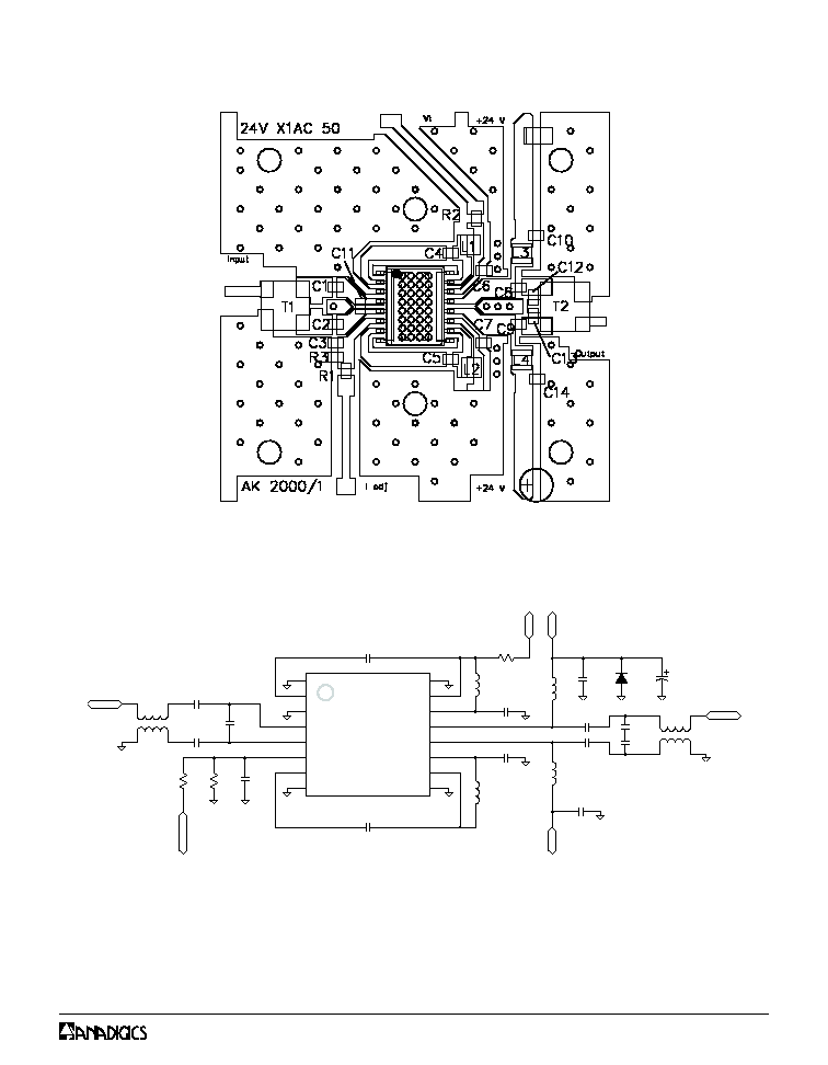
Figure 13: Evaluation Board Layout
Figure 14: Evaluation Board Schematic
R2
C3
ACA2404
2
15
1
10
12
13
11
9
16
14
8
7
6
5
4
3
GND
I
SET
1A
IN
1A
OUT
2A
IN
2A
OUT
GND
GND
GND
Bias 1B
GND
1B
IN
2B
IN
1B
OUT
2B
OUT
Bias 1A
C4
L1
V
t
C6
+24
V
L3
C10
TVS
C15
+24
V
L4
C8
C14
C9
C13
C12
RF OUT
L2
C7
C5
C1
C2
C11
RF IN
R3
R1
I
DD
Ad
ju
st
T1
T2
(+24 V)

10
ADVANCED PRODUCT INFORMATION - Rev 0.0
05/2003
ACA2404
Table 5: Evaluation Board Parts List
Notes:
(1) N connector center pin should be approximately 80 mils in length.
(2) T1, T2 balun: 6.5 turns thru, as shown in Figure 15.
(3) Due to the power dissapation of this device, the printed circuit board should be mounted / attached to a heat sink.
(4) 400 mA minimum current rating.
Figure 15: Balun Drawing
F
E
R
N
O
I
T
P
I
R
C
S
E
D
Y
T
Q
R
O
D
N
E
V
N
/
P
R
O
D
N
E
V
,
7
C
,
6
C
,
3
C
,
2
C
,
1
C
4
1
C
,
0
1
C
1
0
.
0
µ
P
A
C
P
I
H
C
F
7
A
T
A
R
U
M
V
0
5
K
3
0
1
R
7
X
9
3
M
R
G
9
C
,
8
C
,
5
C
,
4
C
P
A
C
P
I
H
C
F
p
0
7
4
4
A
T
A
R
U
M
V
0
5
K
1
7
4
R
7
X
9
3
M
R
G
1
1
C
P
A
C
P
I
H
C
F
p
5
.
0
1
A
T
A
R
U
M
0
5
C
5
R
0
G
O
C
6
3
M
R
G
5
1
C
7
4
µF
P
A
C
.
T
C
E
L
E
1
P
R
O
C
Y
E
K
-I
G
I
D
D
N
-
5
7
2
5
P
3
1
C
,
2
1
C
3
R
,
2
R
,
1
R
,
D
E
S
U
T
O
N
S
V
T
T
T
A
W
0
0
6
T
L
O
V
4
2
S
V
T
1
P
R
O
C
Y
E
K
-I
G
I
D
D
N
-
T
C
C
C
A
4
2
J
B
M
S
1
L
4
L
,
3
L
,
2
L
,
)
4
(
R
O
T
C
U
D
N
I
H
n
0
8
6
4
T
F
A
R
C
L
I
O
C
C
B
K
X
1
8
6
-
S
C
8
0
0
1
1
R
K
5
7
r
o
t
s
i
s
e
R
1
P
R
O
C
Y
E
K
-I
G
I
D
D
N
-
T
C
G
K
5
7
P
R
O
T
C
E
N
N
O
C
)
1
(
5
7
L
E
N
A
P
E
L
A
M
N
T
N
U
O
M
2
K
C
A
N
R
E
T
S
A
P
S
E
S
I
R
P
R
E
T
N
E
4
0
5
4
E
P
2
T
,
1
T
)
2
(
)
N
U
L
A
B
(
F
e
r
o
C
e
ti
r
r
e
2
E
T
I
R
-
R
I
A
F
2
0
7
2
0
0
3
4
8
2
e
r
i
W
.
D
N
I
E
R
I
W
S
W
M
0
2
-
9
2
4
1
6
3
2
-
T
P
d
e
t
n
ir
d
r
a
o
B
ti
u
c
r
i
C
)
3
(
1
D
R
A
D
N
A
T
S
C
N
I
.
C
R
I
C
D
E
T
N
I
R
P
0
5
C
A
1
X
V
4
2
M
U
I
D
N
I
0
0
3
X
S
L
I
M
0
6
1
1
F
O
P
R
O
C
M
U
I
D
N
I
A
C
I
R
E
M
A
Y
6
9
9
4
1
Keep leads twisted
Wrap-around metal
at corners
- or -
vias
Metalized traces on P.C.B.
Pin #1

ADVANCED PRODUCT INFORMATION - Rev 0.0
05/2003
11
ACA2404
Figure 16: S7 Package Outline - 16 Pin Wide Body SOIC with Heat Slug
PACKAGE OUTLINE

WARNING
ANADIGICS products are not intended for use in life support appliances, devices or systems. Use of an ANADIGICS
product in any such application without written consent is prohibited.
IMPORTANT NOTICE
ANADIGICS, Inc.
141 Mount Bethel Road
Warren, New Jersey 07059, U.S.A.
Tel: +1 (908) 668-5000
Fax: +1 (908) 668-5132
URL: http://www.anadigics.com
E-mail: Mktg@anadigics.com
ANADIGICS, Inc. reserves the right to make changes to its products or to discontinue any product at any time without
notice. The product specifications contained in Advanced Product Information sheets and Preliminary Data Sheets are
subject to change prior to a product's formal introduction. Information in Data Sheets have been carefully checked and are
assumed to be reliable; however, ANADIGICS assumes no responsibilities for inaccuracies. ANADIGICS strongly urges
customers to verify that the information they are using is current before placing orders.
ADVANCED PRODUCT INFORMATION - Rev 0.0
05/2003
12
ACA2404
R
E
B
M
U
N
R
E
D
R
O
E
R
U
T
A
R
E
P
M
E
T
E
G
N
A
R
E
G
A
K
C
A
P
N
O
I
T
P
I
R
C
S
E
D
G
N
I
G
A
K
C
A
P
T
N
E
N
O
P
M
O
C
2
P
7
S
4
0
4
2
A
C
A
0
1
1
o
t
0
4
-
o
C
y
d
o
B
e
d
i
W
n
i
P
6
1
g
u
l
S
t
a
e
H
h
ti
w
C
I
O
S
l
e
e
r
d
n
a
e
p
a
t
e
c
e
i
p
0
0
5
,
1
0
P
7
S
4
0
4
2
A
C
A
0
1
1
o
t
0
4
-
o
C
y
d
o
B
e
d
i
W
n
i
P
6
1
g
u
l
S
t
a
e
H
h
ti
w
C
I
O
S
)
e
b
u
t
r
e
p
s
e
c
e
i
p
5
2
(
s
e
b
u
t
c
it
s
a
l
P
ORDERING INFORMATION