AMT128502A
1.25 Gb/s Integrated 850 nm MSM-TIA
Data sheet - Rev. 0
FEATURES
∑
1.25 Gb/s Differential Output TIA
∑
5V Operation
∑
Automatic Gain Control
∑
850nm Photodetector with
100
m
m x 100
m
m
Active Area
∑
Integrated MSM detector & TIA
∑
TO-46 Ultra Flat Window
APPLICATIONS
∑
Gigabit Ethernet (1.250Gb/s)
∑
Fibre Channel (1.0625 Gb/s)
T46F
TO-46 Ultra Flat Window
Package
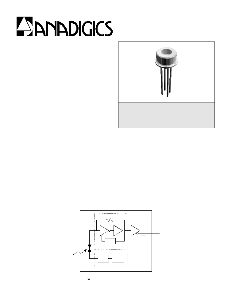
Product Description
The ANADIGICS AMT128502A is a 5V monolithically
integrated Metal-Semiconductor-Metal (MSM)
photodetector and transimpedance amplifier (TIA)
used to convert an 850nm input optical signal into a
differential output voltage, and is manufactured in
ANADIGICS 6 GaAs wafer fabrication facility. The
integrated MSM and TIA receiver maximizes the
receiver performance by minimizing the
photodetector input parasitics to the TIA and
Figure 1: AMT128502A Equivalent Circuit
internally biasing the photodetector to achieve high
sensitivity, bandwidth and overload performance. As
an integrated product the reliability is inherently
better than a discrete solution, and both the MSM-TIA
integrated circuit and TO46 flat window packaged
receiver pass stringent reliability requirements.
These products are readily designed into receivers
and transceivers for Gigabit Ethernet and Fibre
Channel applications.
US Patents: 5047728, 5646573
4K
Charge
Pump
6.5 GHz
Osc
AGC
OUT
OUT
V
DD
4
2
1
3
P
IN

2
AMT128502A
Data Sheet - Revision 0
03/01
V
D
D
V
0
.
7
P
N
I
m
B
d
5
+
T
S
C
∞
5
2
1
o
t
C
∞
5
6
-
.
p
m
e
T
e
g
a
r
o
t
S
Table 1: Absolute Maximum Ratings
(1) Measured at 14 dBm optical input power with output connected into R
L
= 100W
(differential)
(2) Measured at 10
-10
BER with a 2
7
-1 PRBS at 1.25 GB/s
(3) Input optical power = -3 dBm, R
L
= 100 W (differential).
(4) Measured with a 625 MHz, 50% duty cycle square wave.
(5) Measured with a 1.25 Gb/s, 2
7
-1 PRBS.
(6) 1s about the center eye crossing.
(7) 6s about the center eye crossing.
Table 2: Electrical Characteristics
Table 3: Package Pin Description
R
E
T
E
M
A
R
A
P
N
I
M
P
Y
T
X
A
M
T
I
N
U
)
(
h
t
g
n
e
l
e
v
a
W
0
7
7
0
5
8
0
6
8
m
n
a
e
r
A
e
v
it
c
A
r
o
t
c
e
t
e
D
-
0
0
1
x
0
0
1
-
m
µ
2
y
ti
v
i
s
n
o
p
s
e
R
l
a
it
n
e
r
e
ff
i
D
l
a
n
g
i
S
ll
a
m
S
)
1
(
)
z
H
M
0
5
@
(
0
0
0
1
-
-
W
/
V
h
t
d
i
w
d
n
a
B
)
1
(
0
0
0
1
-
0
0
5
1
z
H
M
ff
o
t
u
C
y
c
n
e
u
q
e
r
F
w
o
L
-
0
0
3
0
0
0
1
z
H
k
e
c
n
a
t
s
i
s
e
R
t
u
p
t
u
O
5
2
0
4
0
6
m
h
O
d
a
o
lr
e
v
O
l
a
c
it
p
O
)
2
(
0
-
-
m
B
d
y
ti
v
it
i
s
n
e
S
l
a
c
it
p
O
)
2
(
0
2
-
2
2
-
m
B
d
e
g
a
tl
o
V
t
u
p
t
u
O
l
a
it
n
e
r
e
ff
i
D
)
4
(
,)
3
(
-
0
0
7
-
V
m
T
E
S
I
R
T
&
L
L
A
F
)
%
0
8
-
0
2
(
)
4
(
,)
3
(
-
0
6
2
-
s
p
n
o
it
r
o
t
s
i
D
e
l
c
y
C
y
t
u
D
)
5
(
,)
3
(
-
4
0
1
%
r
e
tt
i
J
S
M
R
)
6
(
,)
5
(
,)
3
(
-
5
1
-
s
p
)
k
p
-
k
p
(
r
e
tt
i
J
l
a
t
o
T
)
7
(
,)
5
(
,)
3
(
-
0
9
-
s
p
t
n
e
rr
u
C
y
l
p
p
u
S
-
-
0
5
A
m
e
g
n
a
R
e
g
a
tl
o
V
g
n
it
a
r
e
p
O
5
.
4
+
0
.
5
+
5
.
5
+
V
e
g
n
a
R
e
r
u
t
a
r
e
p
m
e
T
t
n
e
i
b
m
A
g
n
it
a
r
e
p
O
0
-
0
7
C
∞
l
N
I
P
n
o
it
p
i
r
c
s
e
D
t
n
e
m
m
o
C
1
V
T
U
O
)
d
e
tr
e
v
n
i
-
n
o
n
(
e
g
a
tl
o
V
t
u
p
t
u
O
A
I
T
-
t
u
p
n
i
l
a
c
it
p
o
h
ti
w
'
1
'
l
a
c
i
g
o
L
2
V
D
D
e
g
a
tl
o
V
y
l
p
p
u
S
e
v
it
i
s
o
P
-
s
tl
o
V
5
+
3
V
T
U
O
)
d
e
tr
e
v
n
i(
e
g
a
tl
o
V
t
u
p
t
u
O
A
I
T
-
t
u
p
n
i
l
a
c
it
p
o
h
ti
w
'
0
'
l
a
c
i
g
o
L
4
d
n
u
o
r
G
d
e
d
n
u
o
r
g
s
i
e
s
a
C

AMT128502A
3
Data Sheet - Revision 0
03/01
10mV/Div 200ps/Div
150mV/Div. 200ps/Div
Figure 2: Eye Diagram with an Optical Input
Power of -17dBm
Figure 3: Eye Diagram with an Optical Input
Power of -1.0dBm
Figure 4: Supply Current vs. Temperature
Figure 5: Bandwidth vs. Temperature
Figure 6: Differential Responsivity vs.
Temperature
20.0
25.0
30.0
35.0
40.0
45.0
50.0
0
20
40
60
80
100
Ambient Temperature (C)
Supply C
u
r
r
ent
(
m
A)
4.5V
5.0V
5.5V
600
800
1000
1200
1400
1600
0
20
40
60
80
100
Ambient Temperature (C)
Bandw
idt
h
(
M
H
z
)
4.5V
5.0V
5.5V
-24.0
-23.5
-23.0
-22.5
-22.0
-21.5
-21.0
-20.5
-20.0
0
20
40
60
80
100
Ambient Temperature (C)
Sens
it
iv
it
y
(
d
Bm
)
4.5V
5.0V
5.5V
1000
1200
1400
1600
1800
2000
0
20
40
60
80
100
Ambient Temperature (C)
Di
f
f
e
r
ent
i
a
l
Responsi
v
i
t
y (
V
/
W
)
4.5V
5.0V
5.5V
Figure 7: Sensitivity vs. Temperature

AMT128502A
5
Data Sheet - Revision 0
03/01
V
OUT
V
OUT
DUT
0.1 uF
0.1uF
0.1uF
V
DD
Figure 11: DUT Test Fixture Schematic
Figure 12: Application Schematic
LIMITING
AMPLIFIER
4K
Charge
Pump
AGC
OUT
OUT
V
DD
4
2
1
3
0.1uF
0.1uF
C
F
R
O
0.1uF
6.5 GHz
OSC
C
F
is an optional single pole noise filter
f
c
is the desired cutoff frequency
R
= 50 W
R
O
is required with high input resistance limiting amplifiers
R
O
= 100 W
f
c
R
C
F
=
2
1
