 | –≠–ª–µ–∫—Ç—Ä–æ–Ω–Ω—ã–π –∫–æ–º–ø–æ–Ω–µ–Ω—Ç: ATA06212A | –°–∫–∞—á–∞—Ç—å:  PDF PDF  ZIP ZIP |

08/2001
ATA06212A
AGC Transimpedance Amplifier
PRELIMINARY DATA SHEET- Rev 1.2
D1
FEATURES
∑
Single +5 Volt Supply
∑
Automatic Gain Control
∑
- 34 dBm Sensitivity
∑
0 dBm Optical Overload
∑
425 MHz Bandwidth
APPLICATIONS
∑
SONET OC-12/SDH STM-4 (622 Mb/s)
Receiver
∑
Low Noise RF Amplifier
Vdd2
GND
GND
GND
GND
GND
GND
GND
GND
V out
I in
Vdd2
CBY
CBY
CAGC
Vdd1
PRODUCT DESCRIPTION
Figure 1: Equivalent Circuit
AGC
I
IN
GND
or
neg. supply
GND
V
OUT
V
DD
Photodetector cathode must be connected to
I
IN
for proper AGC operation
The ANADIGICS ATA06212A is a 5V low noise
transimpedance amplifier with AGC designed to be
used in OC-12/STM-4 fiber optic links. The device is
used in conjunction with a photodetector (PIN diode
or avalanche photodiode) to convert an optical signal
into an output voltage. The ATA06212A offers a
bandwidth of 425MHz and a dynamic range of 35dB.
It is manufactured in a GaAs MESFET process and
is available in bare die form.

PRELIMINARY DATA SHEET - Rev 1.2
08/2001
2
ATA06212A
Table 1: ATA06212AD1C Pad Description
D
A
P
D
N
O
I
T
P
I
R
C
S
E
C
T
N
E
M
M
O
V
1
D
D
1
D
D
V
e
g
a
t
s
n
i
a
g
t
u
p
n
i
r
o
f
y
l
p
p
u
s
e
v
it
i
s
o
P
V
2
D
D
2
D
D
V
e
g
a
t
s
n
i
a
g
d
n
o
c
e
s
r
o
f
y
l
p
p
u
s
e
v
it
i
s
o
P
I
N
I
t
n
e
r
r
u
C
t
u
p
n
I
A
I
T
n
o
it
a
r
e
p
o
r
e
p
o
r
p
r
o
f
e
d
o
h
t
a
c
r
o
t
c
e
t
e
d
o
t
t
c
e
n
n
o
C
V
T
U
O
e
g
a
tl
o
V
t
u
p
t
u
O
A
I
T
k
c
o
l
b
C
D
l
a
n
r
e
t
x
e
s
e
r
i
u
q
e
R
C
C
G
A
r
o
ti
c
a
p
a
C
C
G
A
l
a
n
r
e
t
x
E
C
+
F
p
5
.
4
(
x
k
0
7
C
G
A
t
n
a
t
s
n
o
c
e
m
it
C
G
A
=
)
C
Y
B
r
o
ti
c
a
p
a
c
s
s
a
p
y
b
e
g
a
t
s
n
i
a
g
t
u
p
n
I
F
p
6
5
>
Figure 2: Bonding Pad
V
DD2
GND
GND
GND
GND
GND
GND
GND
CAGC
V
OUT
I
IN
V
DD2
CBY
CBY
GND
V
DD1
AN14T
925um
1250um
100um
100um
Table 2: Absolute Maximum Ratings
V
1
D
D
V
0
.
7
V
2
D
D
V
0
.
7
I
N
I
A
m
5
T
A
C
∞
5
2
1
o
t
C
∞
0
4
-
.
p
m
e
T
g
n
it
a
r
e
p
O
T
S
C
∞
0
5
1
o
t
C
∞
5
6
-
.
p
m
e
T
e
g
a
r
o
t
S
ELECTRICAL CHARACTERISTICS
Stresses in excess of the absolute ratings may cause
permanent damage. Functional operation is not
implied under these conditions. Exposure to absolute
ratings for extended periods of time may adversely
affect reliability.

3
PRELIMINARY DATA SHEET - Rev 1.2
08/2001
ATA06212A
Table 3: Electrical Characteristics (1)
(T
A
= 25∞C, V
DD
=+5.0V + 10%, C
DIODE
+C
STRAY
= 0.7 pF, Detector Cathode to I
IN
)
Notes:
(1) f = 50 MHz
(2) Measured with I
IN
below AGC Threshold.
During AGC, input impedance will decrease proportionally to I
IN.
(3) Defined as the I
IN
where Transresistance has decreased by 50%.
(4) See note on "Indirect Measurement of Optical Overload."
(5) See note on "Input Referred Noise Current."
(6) C
AGC
= 56 pF
(7) Parameter is guaranteed (not tested) by
design and characterization data @ 622 Mb/s, assuming detector responsively
of 0.95.
R
E
T
E
M
A
R
A
P
N
I
M
P
Y
T
X
A
M
T
I
N
U
R
(
e
c
n
a
t
s
i
s
e
r
s
n
a
r
T
L
I,
=
C
D
)
A
n
0
0
5
<
7
1
1
-
K
R
(
e
c
n
a
t
s
i
s
e
r
s
n
a
r
T
L
)
0
5
=
)
1
(
5
.
3
5
-
K
B
d
3
-
h
t
d
i
w
d
n
a
B
0
0
4
5
2
4
-
z
H
M
e
c
n
a
t
s
i
s
e
R
t
u
p
n
I
)
2
(
-
0
0
3
-
e
c
n
a
t
s
i
s
e
R
t
u
p
t
u
O
0
3
3
4
0
6
e
g
a
tl
o
V
t
e
s
ff
O
t
u
p
n
I
0
.
1
3
.
1
-
s
tl
o
V
e
g
a
tl
o
V
t
e
s
ff
O
t
u
p
t
u
O
0
.
1
4
.
1
-
s
tl
o
V
I
(
d
l
o
h
s
e
r
h
T
C
G
A
N
I
)
)
3
(
-
0
4
-
A
t
n
a
t
s
n
o
C
e
m
i
T
C
G
A
)
6
(
-
2
.
4
-
d
a
o
lr
e
v
O
l
a
c
it
p
O
)
4
(
0
1
+
-
m
B
d
y
ti
v
it
i
s
n
e
S
l
a
c
it
p
O
)
7
(
-
4
3
-
-
m
B
d
t
n
e
r
r
u
C
e
s
i
o
N
t
u
p
n
I
)
5
(
-
0
4
0
5
A
n
t
n
e
r
r
u
C
y
l
p
p
u
S
-
0
3
5
4
A
m
e
g
n
a
R
e
g
a
tl
o
V
g
n
it
a
r
e
p
O
5
.
4
+
0
.
5
+
0
.
6
+
s
tl
o
V
e
g
n
a
R
e
r
u
t
a
r
e
p
m
e
T
g
n
it
a
r
e
p
O
0
4
-
-
5
8
o
C
µ
sec
µ

PRELIMINARY DATA SHEET - Rev 1.2
08/2001
4
ATA06212A
Figure 3: Typical Bonding Diagram
Note: Bond to either V
DD2
Bond Pad
56 pF
56 pF
56 pF
56 pF
PIN
OUT
V
DD
V
DD2
GND
GND
GND
GND
GND
GND
GND
CAGC
V
OUT
I
IN
V
DD2
CBY
CBY
GND
V
DD1
AN14T
5
PRELIMINARY DATA SHEET - Rev 1.2
08/2001
ATA06212A
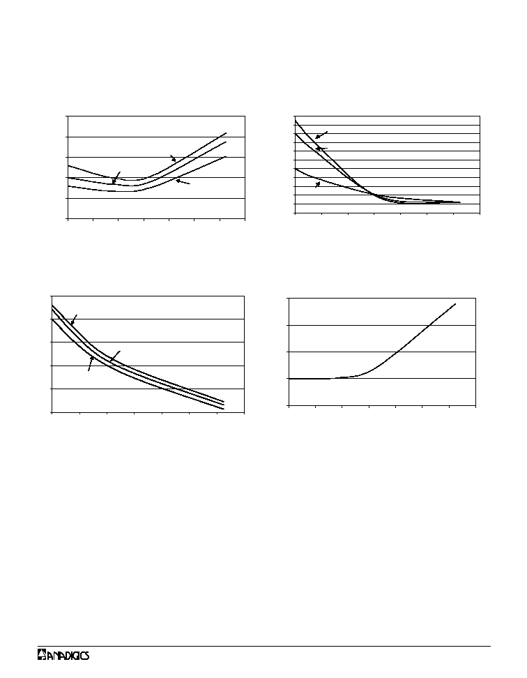
PERFORMANCE DATA (V
DD
= +5V, T
A
= +25∞C, UNLESS OTHERWISE NOTED)
1400.0
1500.0
1600.0
1700.0
1800.0
1900.0
2000.0
2100.0
2200.0
2300.0
2400.0
2500.0
-40
-20
0
20
40
60
80
100
Temperature (∞C)
(M
H
z
)
C
T
= 0.6 pF; I
IN
= 1.5 mA (Average)
VDD = 5.0V
VDD = 5.5V
VDD = 4.5V
350.0
400.0
450.0
500.0
550.0
600.0
-40
-20
0
20
40
60
80
100
Temperature (∞C)
B
a
ndw
i
d
th (M
H
z
)
C
T
= 0.6 pF
VDD = 5.5V
VDD = 4.5V
VDD = 5.0V
1.2
1.3
1.4
1.5
1.6
1.7
-40
-20
0
20
40
60
80
100
Temperature (∞C)
(V)
VDD = 5.0V
VDD = 4.5V
VDD = 5.5V
30.0
35.0
40.0
45.0
50.0
-40
-20
0
20
40
60
80
100
Temperature (∞C)
I
nput
R
e
f
e
rre
d N
o
i
s
e
(
n
A
R
M
S
CT = 0.5 pF; 467 MHz LPF
Figure 4: 3dB Bandwidth vs. Temperature
Figure 5: AGC Bandwidth vs. Temperature
Figure 7: Input Referred Noise vs. Temperature
Figure 6: Input Offset Voltage vs. Temperature