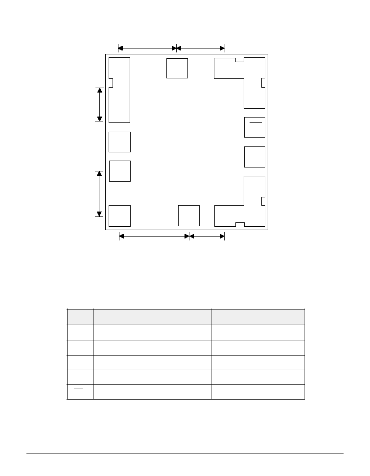
06-01
D1
Die Package
FEATURES
∑
10 Gb/s Differential Output TIA
∑
+5V Power Supply
∑
Low Group Delay
∑
Small Size: 0.95mm x 1.014mm
∑
340mW (typ) power dissipation
APPLICATIONS
∑
SONET OC-192
∑
10 Gb/s DWDM
∑
10 Gb/s Ethernet
PRODUCT DESCRIPTION
ATA7601
5.0V 10 Gb/s TIA
PRELIMINARY DATA SHEET - Rev 2
The ANADIGICS ATA7601D1 is a 5V high-speed
transimpedance amplifier (TIA) for 10 Gb/s
applications available in bare die form and
manufactured using an InGaP HBT process.
The device is used in conjunction with a
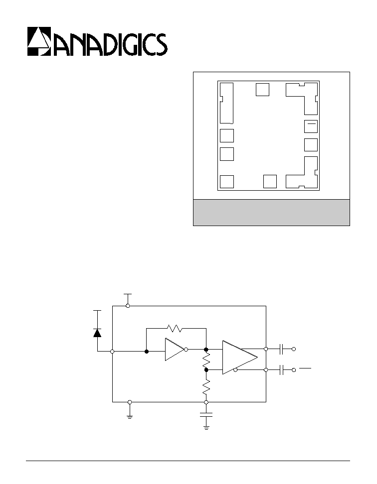
Figure 1: Circuit Block Diagram
GND
GND
GND
GND
GND
V
CC
V
OUT
V
OUT
C
EXT
I
IN
photodetector to convert an optical signal into a
differential voltage that must be AC coupled to a post
amplifier. With its low input noise, a sensitivity of
better than -19dBm (BER <10
-10
) can be achieved
with the ATA7601D1.
V
OUT
V
OUT
V
CC
C
EXT
V
BIAS
I
IN

8
PRELIMINARY DATA SHEET - Rev 2
06-01
ATA7601
Packaging
The ATA7601D1 is provided as bare die. For optimum
performance, the die should be packaged in a
hermetic enclosure and a low inductance ground
plane should be made available for power supply
bypassing and ground bonds. When packaging the
ATA7601D1, the temperature of the die must be kept
below 260
∞
C to ensure the device reliability. The
ATA7601D1 has backside metal and can be epoxy
mounted or solder attached. A good thermally
conductive, silver filled epoxy is recommended for
epoxy mounting. If a solder attach is being used, the
die attach temperature must be kept less than 260
∞
C
to ensure the device reliability. A soft silicon/rubber
tip collet or pyramidal collet should be used for die
mounting, although tweezers can be used with
extreme care.
Thermosonic ball bonding, at a stage temperature
of 150 to 175
∞
C with 1 to 1.3 mil gold wire, is the
recommended interconnect technique. The bond
force, time and ultrasonic power are all critical
parameters and may require optimization to achieve
the correct bond without causing bonding pad
delamination or damage under the bonding pad.
The bond wire from the photodetector to I
IN
should
be made as short as possible. As the inductance of
this connection increases beyond 1nH, more gain
peaking will occur and the group delay performance
will degrade.
Output Connections
The ATA7601D1 provides a differential output that
must be AC coupled to the next stage of the receiver
as the output buffer is not designed to drive a DC
coupled 50W load. For single-ended applications,
one output of the ATA7601D1 must be AC terminated
to a 50W load.
C
EXT
Connection
In order to achieve the desired low frequency cutoff,
an external capacitor is required. A low inductance
surface mount chip capacitor or MIM capacitor is
recommended.
Sensitivity Measurement
The typical sensitivity, as specified in the AC
characteristics, is 19.0dBm. This was measured
at a BER of 10
-10
with a 10Gb/s, 2
23
-1 PRBS, using a
lensed single mode fiber with the photodetector and
TIA in an open test fixture under the following
conditions:
Photodetector active area: 32mm
Photodetector capacitance: 0.2pF
Photodetector responsivity: 0.80A/W
Lensed fiber beam width: 13mm (86.5% of
contained power)
Lensed fiber focal distance: 3mm
When the photodetector and TIA are packaged in a
hermetic enclosure, with the fiber optimally aligned
to the active area of the photodiode, an improvement
in sensitivity should be observed.
Device Modeling and Simulation
S-parameter files of the TIA are available on the
ANADIGICS web site (
http://www.anadigics.com
) or
upon request. Also included on the web-site is a
virtual sample. This is an encrypted model of the
TIA that can be downloaded into the ADS simulation
environment.

12
IMPORTANT NOTICE
ANADIGICS, Inc. reserves the right to make changes to its products or to discontinue any product at any time without
notice. The product specifications contained in Advanced Product Information sheets and Preliminary Data Sheets are
subject to change prior to a products formal introduction. Information in Data Sheets have been carefully checked and are
assumed to be reliable; however, ANADIGICS assumes no responsibilities for inaccuracies. ANADIGICS strongly urges
customers to verify that the information they are using is current before placing orders.
WARNING
ANADIGICS products are not intended for use in life support appliances, devices, or systems. Use of an ANADIGICS
product in any such application without written consent is prohibited.
ANADIGICS, Inc.
141 Mount Bethel Road
Warren, New Jersey 07059, U.S.A
Tel: +1 (908) 668-5000
Fax: +1 (908) 668-5132
http://www.anadigics.com
Mktg@anadigics.com
PRELIMINARY DATA SHEET - Rev 2
06-01
ATA7601
ORDERING INFORMATION
R
E
B
M
U
N
T
R
A
P
N
O
I
T
P
O
E
G
A
K
C
A
P
N
O
I
T
P
I
R
C
S
E
D
E
G
A
K
C
A
P
C
1
D
1
0
6
7
A
T
A
1
D
e
i
D