
01/2006
AWM6430
3.3-3.6 GHz WiMAX Power Amplifier Module
PRELIMINARY DATA SHEET- Rev 1.0
M18 Package
12 Pin 4.5 mm x 4.5 mm x 1.4 mm
Surface Mount Module
FEATURES
∑
27 dB Gain
∑
+24 dBm Linear Output Power
∑
2.3 % EVM (OFDM Modulation)
∑
+5 V to +6 V Supply
∑
High Efficiency
∑
Integrated Step Attenuator
∑
Integrated Output Power Detector
∑
50
Matched RF Ports
∑
RoHS Compliant 4.5 mm x 4.5 mm x 1.4 mm
Surface Mount Module
APPLICATIONS
∑
WiMAX tranceivers that support the IEEE
802.16-2004 and ETSI EN301-021 standards
∑
Broadband Wireless Applications (BWA)
PRODUCT DESCRIPTION
The ANADIGICS AWM6430 WiMAX Power Amplifier
is a high performance device that delivers
exceptional linearity and efficiency at high levels of
output power. Designed to operate in the 3.5 GHz
band, it supports the IEEE 802.16-2004 and ETSI
EN301-021 wireless standards.
The device requires only a single +5 V to +6 V supply
and a low-current reference input. An integrated
detector can be used to monitor output power, and
an integrated 20 dB step attenuator enables gain
control. No external circuits are required for biasing
or RF impedance matching, thus reducing external
component costs and facilitating circuit board
designs.
The AWM6430 is manufactured using advanced
InGaP HBT technology that offers state-of-the-art
reliability, temperature stability and ruggedness. It
is optimized for use in a 50
system, and is offered
in a 4.5 mm x 4.5 mm x 1.4 mm surface mount
module.
Figure 1: Functional Block Diagram
Step
Attenuator
Power
Detector
Bias
Control
Supply
Voltage
Supply
Voltage
Attenuator
Control
Detector
Ouput
RF Input
RF Output
Matching
Network
Bias
Voltage
Ground
AWM6430
AWM6430

2
PRELIMINARY DATA SHEET - Rev 1.0
01/2006
AWM6430
Figure 2: Pinout (X-ray Top View)
Table 1: Pin Description
N
I
P
E
M
A
N
N
O
I
T
P
I
R
C
S
E
D
1
V
C
C
e
g
a
tl
o
V
y
l
p
p
u
S
2
F
R
N
I
t
u
p
n
I
F
R
3
D
N
G
d
n
u
o
r
G
4
V
S
A
I
B
n
w
o
d
t
u
h
S
/
s
a
i
B
5
V
C
C
e
g
a
tl
o
V
y
l
p
p
u
S
6
V
N
T
T
A
l
o
r
t
n
o
C
r
o
t
a
u
n
e
tt
A
7
T
E
D
t
u
p
t
u
O
r
o
t
c
e
t
e
D
8
D
N
G
d
n
u
o
r
G
9
D
N
G
d
n
u
o
r
G
0
1
F
R
T
U
O
t
u
p
t
u
O
F
R
1
1
D
N
G
d
n
u
o
r
G
2
1
V
C
C
e
g
a
tl
o
V
y
l
p
p
u
S
V
CC
RF
OUT
V
BIAS
RF
IN
DET
GND
1
GND
10
2
3
4
5
6
9
8
7
V
CC
GND
GND
GND
12
11
V
CC
V
ATTN

PRELIMINARY DATA SHEET - Rev 1.0
01/2006
AWM6430
3
ELECTRICAL CHARACTERISTICS
Table 2: Absolute Minimum and Maximum Ratings
Stresses in excess of the absolute ratings may cause permanent damage. Functional operation is not
implied under these conditions. Exposure to absolute ratings for extended periods of time may adversely
affect reliability.
Table 3: Operating Ranges
The device may be operated safely over these conditions; however, parametric performance is guaranteed
only over the conditions defined in the electrical specifications.
R
E
T
E
M
A
R
A
P
N
I
M
P
Y
T
X
A
M
T
I
N
U
S
T
N
E
M
M
O
C
)
f
(
y
c
n
e
u
q
e
r
F
g
n
it
a
r
e
p
O
0
0
3
3
-
0
0
6
3
z
H
M
V
(
e
g
a
tl
o
V
y
l
p
p
u
S
C
C
)
0
.
5
+
-
0
.
6
+
V
V
(
e
g
a
tl
o
V
s
a
i
B
S
A
I
B
)
9
.
2
+
0
0
.
3
+
-
1
.
3
+
7
.
0
+
V
"
n
o
"
A
P
"
n
w
o
d
t
u
h
s
"
A
P
V
(
e
g
a
tl
o
V
l
o
r
t
n
o
C
r
o
t
a
u
n
e
tt
A
N
T
T
A
)
h
g
i
H
c
i
g
o
L
w
o
L
c
i
g
o
L
3
.
2
+
0
-
-
7
.
3
+
7
.
0
+
V
d
e
l
b
a
n
e
r
o
t
a
u
n
e
tt
A
n
i
a
g
l
a
n
i
m
o
N
P
(
r
e
w
o
P
t
u
p
t
u
O
F
R
T
U
O
)
-
4
2
+
-
m
B
d
T
(
e
r
u
t
a
r
e
p
m
e
T
e
s
a
C
C
)
0
4
-
-
5
8
+
C
∞
R
E
T
E
M
A
R
A
P
N
I
M
X
A
M
T
I
N
U
S
T
N
E
M
M
O
C
V
(
e
g
a
tl
o
V
y
l
p
p
u
S
C
C
)
0
5
.
6
+
V
V
(
e
g
a
tl
o
V
s
a
i
B
S
A
I
B
)
0
3
.
3
+
V
V
(
e
g
a
tl
o
V
l
o
r
t
n
o
C
r
o
t
a
u
n
e
tt
A
N
T
T
A
)
0
7
.
3
+
V
r
e
w
o
P
t
u
p
n
I
F
R
-
0
m
B
d
l
a
n
g
i
s
d
e
t
a
l
u
d
o
m
M
D
F
O
g
n
it
a
R
D
S
E
A
1
s
s
a
l
C
3
s
s
a
l
C
-
-
-
-
M
B
H
M
D
C
l
e
v
e
L
L
S
M
3
4
-
-
-
-
5
3
2
C
∞
w
o
lf
e
R
k
a
e
P
0
5
2
C
∞
w
o
lf
e
R
k
a
e
P
e
r
u
t
a
r
e
p
m
e
T
e
g
a
r
o
t
S
0
4
-
0
5
1
+
C
∞

4
PRELIMINARY DATA SHEET - Rev 1.0
01/2006
AWM6430
Table 4: Electrical Specifications
(T
C
= +25 ∞C, V
CC
= +6.0 V, V
BIAS
= +3.0 V, f = 3.5 GHz, 50
system)
R
E
T
E
M
A
R
A
P
N
I
M
P
Y
T
X
A
M
T
I
N
U
S
T
N
E
M
M
O
C
n
i
a
G
5
2
7
2
0
3
B
d
p
e
t
S
r
o
t
a
u
n
e
tt
A
5
1
7
1
9
1
B
d
k
s
a
M
m
u
r
t
c
e
p
S
s
t
e
e
M
r
e
w
o
P
t
u
p
t
u
O
4
2
+
-
-
m
B
d
G
e
p
y
T
1
2
0
-
1
0
3
N
E
I
S
T
E
M
V
E
-
3
.
2
5
.
2
%
P
m
B
d
4
2
+
t
a
T
U
O
B
d
1
P
t
u
p
t
u
O
-
1
3
+
-
m
B
d
W
C
3
P
I
t
u
p
t
u
O
-
3
4
+
-
m
B
d
m
B
d
1
2
+
,
s
e
n
o
t
W
C
o
w
t
e
n
o
t
r
e
p
t
u
p
t
u
o
s
c
i
n
o
m
r
a
H
-
0
2
-
-
m
B
d
P
m
B
d
4
2
+
t
a
T
U
O
y
c
n
e
i
c
if
f
E
d
e
d
d
A
-
r
e
w
o
P
-
8
.
2
1
-
%
P
m
B
d
4
2
+
t
a
T
U
O
e
g
a
tl
o
V
r
o
t
c
e
t
e
D
r
e
w
o
P
P
m
B
d
4
2
+
t
a
T
U
O
P
m
B
d
4
1
+
t
a
T
U
O
-
-
6
.
2
+
6
.
0
+
-
-
V
d
a
o
l
e
c
n
a
d
e
p
m
i
h
g
i
H
t
n
e
r
r
u
C
t
n
e
c
s
e
i
u
Q
-
7
8
0
2
1
A
m
n
o
it
p
m
u
s
n
o
C
t
n
e
r
r
u
C
V
C
C
V
S
A
I
B
V
N
T
T
A
-
-
-
5
0
3
8
.
6
2
.
0
5
6
3
8
0
.
1
A
m
P
T
U
O
m
B
d
4
2
+
=
V
3
.
3
+
=
h
g
i
H
c
i
g
o
L
t
n
e
r
r
u
C
e
g
a
k
a
e
L
-
7
.
1
0
.
3
A
m
V
(
n
w
o
d
t
u
h
s
A
P
S
A
I
B
)
V
0
=
Note:
1. All RF measurements performed with an 802.11g 54 Mbps OFDM signal unless otherwise noted.

PRELIMINARY DATA SHEET - Rev 1.0
01/2006
AWM6430
5
PERFORMANCE DATA
Figure 3: Gain vs. Output Power
(T
C
= +25 ∞C, V
CC
= +6.0 V, V
BIAS
= +3.0 V,
f = 3.5 GHz, 54 Mbps OFDM Modulation)
Figure 4: Gain vs. Frequency
(T
C
= +25 ∞C, V
CC
= +6.0 V, V
BIAS
= +3.0 V,
P
OUT
= +24 dBm, 54 Mbps OFDM Modulation)
Figure 5: Uncorrected EVM vs. Output Power
(T
C
= +25 ∞C, V
CC
= +6.0 V, V
BIAS
= +3.0 V, 54 Mbps
OFDM Modulation, system EVM Approx. 0.8 %)
Figure 6: Uncorrected EVM vs. Frequency
(T
C
= +25 ∞C, V
CC
= +6.0 V, V
BIAS
= +3.0 V, 54 Mbps
OFDM Modulation, system EVM Approx. 0.8 %)
25.0
25.5
26.0
26.5
27.0
27.5
28.0
28.5
29.0
29.5
30.0
13
14
15
16
17
18
19
20
21
22
23
24
25
26
Output Power (dBm)
Gain (dB)
25.0
25.5
26.0
26.5
27.0
27.5
28.0
28.5
29.0
29.5
30.0
3.25
3.30
3.35
3.40
3.45
3.50
3.55
3.60
3.65
Frequency (GHz)
Gain (dB)
0
1
2
3
4
5
6
7
13
14
15
16
17
18
19
20
21
22
23
24
25
26
Output Power (dBm)
EVM (%)
3.30 GHz
3.35 GHz
3.40 GHz
3.45 GHz
3.50 GHz
3.55 GHz
3.60 GHz
Frequency
0
1
2
3
4
5
6
7
3.25
3.30
3.35
3.40
3.45
3.50
3.55
3.60
3.65
Frequency (GHz)
EVM (%)
+24 dBm
+23 dBm
+22 dBm
Output Power
0.0
0.5
1.0
1.5
2.0
2.5
3.0
13
14
15
16
17
18
19
20
21
22
23
24
25
26
Output Power (dBm)
Detector Voltage (V)
0.0
0.5
1.0
1.5
2.0
2.5
3.0
3.25
3.30
3.35
3.40
3.45
3.50
3.55
3.60
3.65
Frequency (GHz)
Detector Voltage (V)
+24 dBm
+21 dBm
+18 dBm
+15 dBm
Output Power
Figure 7: Detector Voltage vs. Output Power
(T
C
= +25 ∞C, V
CC
= +6.0 V, V
BIAS
= +3.0 V,
f = 3.5 GHz, 54 Mbps OFDM Modulation)
Figure 8: Detector Voltage vs. Frequency
(T
C
= +25 ∞C, V
CC
= +6.0 V, V
BIAS
= +3.0 V,
54 Mbps OFDM Modulation)

6
PRELIMINARY DATA SHEET - Rev 1.0
01/2006
AWM6430
Figure 9: Effects of Bias Voltage (V
BIAS
) on EVM
(T
C
= +25 ∞C, V
CC
= +6.0 V, f = 3.5 GHz, 54 Mbps
OFDM Modulation, system EVM Approx. 0.8 %)
Figure 10: Effects of Supply Voltage (V
CC
) on EVM
(T
C
= +25 ∞C, V
BIAS
= +3.0 V, f = 3.5 GHz, 54 Mbps
OFDM Modulation, system EVM Approx. 0.8 %)
Figure 11: Effects of Case Temperature on EVM
(V
CC
= +6.0 V, V
BIAS
= +3.0 V, f = 3.5 GHz, 54 Mbps
OFDM Modulation, system EVM Approx. 0.8 %)
0
1
2
3
4
5
6
7
13
14
15
16
17
18
19
20
21
22
23
24
25
26
Output Power (dBm)
EVM (%)
2.80V
2.85V
2.90V
2.95V
3.00V
3.05V
3.10V
Bias Voltage
0
1
2
3
4
5
6
7
13
14
15
16
17
18
19
20
21
22
23
24
25
26
Output Power (dBm)
EVM (%)
6.0 V
5.5 V
5.0 V
Vcc
0
1
2
3
4
5
6
7
12
13
14
15
16
17
18
19
20
21
22
23
24
25
26
Output Power (dBm)
EVM (%)
+85 deg C
+50 deg C
+25 deg C
0 deg C
-25 deg C
-40 deg C
Case Temperature

PRELIMINARY DATA SHEET - Rev 1.0
01/2006
AWM6430
7
Figure 14: Supply Current vs. Output Power
(T
C
= +25 ∞C, V
CC
= +6.0 V, V
BIAS
= +3.0 V,
f = 3.5 GHz, 54 Mbps OFDM Modulation)
Figure 12: Gain vs. Bias Voltage (V
BIAS
)
(T
C
= +25 ∞C, V
CC
= +6.0 V, f = 3.5 GHz,
54 Mbps OFDM Modulation)
Figure 13: Gain vs. Case Temperature
(V
CC
= +6.0 V, V
BIAS
= +3.0 V, f = 3.5 GHz,
P
OUT
= +23 dBm, 54 Mbps OFDM Modulation)
Figure 15: Supply Current vs. Case Temperature
(V
CC
= +6.0 V, V
BIAS
= +3.0 V, f = 3.5 GHz,
P
OUT
= +23 dBm 54 Mbps OFDM Modulation)
25.0
25.5
26.0
26.5
27.0
27.5
28.0
28.5
29.0
29.5
30.0
2.75
2.80
2.85
2.90
2.95
3.00
3.05
3.10
3.15
Bias Voltage (V)
Gain (dB)
25.0
25.5
26.0
26.5
27.0
27.5
28.0
28.5
29.0
29.5
30.0
-50
-40
-30
-20
-10
0
10
20
30
40
50
60
70
80
90
Case Temperature (
o
C )
Gain (dB)
100
150
200
250
300
350
400
13
14
15
16
17
18
19
20
21
22
23
24
25
26
Output Power (dBm)
Icc (mA)
250
260
270
280
290
300
-50
-40
-30
-20
-10
0
10
20
30
40
50
60
70
80
90
Case Temperature (
o
C )
Icc (mA)
8
PRELIMINARY DATA SHEET - Rev 1.0
01/2006
AWM6430
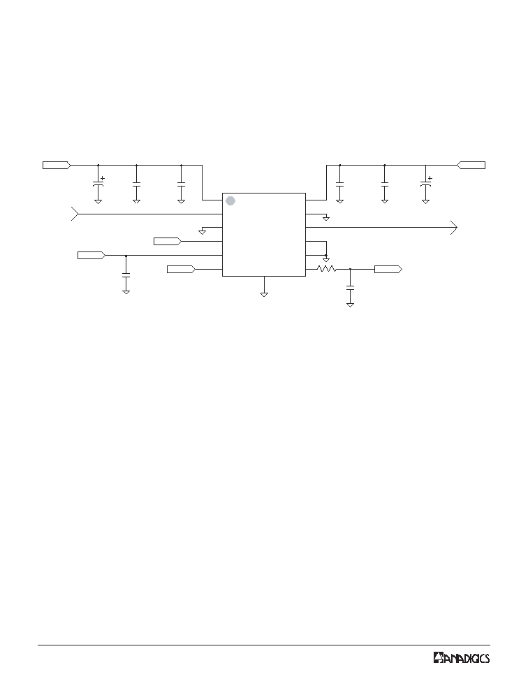
APPLICATION INFORMATION
Transmit Disable and Attenuator Control
The power amplifier is disabled by setting V
BIAS
below +0.7 V. The step attenuator is enabled by
applying a logic high to V
ATTN
; the PA exhibits nominal
gain when a logic low is applied to V
ATTN
.
Figure 16: Application Circuit
GND
at slug
RF IN
2
9
1
6
7
12
8
5
4
3
V
CC
V
BIAS
GND
RF
IN
GND
V
CC
GND
V
CC
GND
RF
OUT
V
CC
V
CC
RF OUT
V
ATTN
DET
V
CC
V
ATTN
DET
OUT
4.7 K
V
BIAS
10
11
2.2
µ
F
150 pF
6.8 pF
0.1
µ
F
0.01
µ
F
1
µ
F
2.2
µ
F
0.1
µ
F

PRELIMINARY DATA SHEET - Rev 1.0
01/2006
AWM6430
9
Figure 17: Land Pattern

10
PRELIMINARY DATA SHEET - Rev 1.0
01/2006
AWM6430
PACKAGE OUTLINE
Figure 18: M18 Package Outline - 12 Pin 4.5 mm x 4.5 mm x 1.4 mm Surface Mount Module

PRELIMINARY DATA SHEET - Rev 1.0
01/2006
AWM6430
11
NOTES

WARNING
ANADIGICS products are not intended for use in life support appliances, devices or systems. Use of an ANADIGICS
product in any such application without written consent is prohibited.
IMPORTANT NOTICE
ANADIGICS, Inc.
141 Mount Bethel Road
Warren, New Jersey 07059, U.S.A.
Tel: +1 (908) 668-5000
Fax: +1 (908) 668-5132
URL: http://www.anadigics.com
E-mail: Mktg@anadigics.com
ANADIGICS, Inc. reserves the right to make changes to its products or to discontinue any product at any time without
notice. The product specifications contained in Advanced Product Information sheets and Preliminary Data Sheets are
subject to change prior to a product's formal introduction. Information in Data Sheets have been carefully checked and are
assumed to be reliable; however, ANADIGICS assumes no responsibilities for inaccuracies. ANADIGICS strongly urges
customers to verify that the information they are using is current before placing orders.
PRELIMINARY DATA SHEET - Rev 1.0
01/2006
12
AWM6430
R
E
B
M
U
N
R
E
D
R
O
E
R
U
T
A
R
E
P
M
E
T
E
G
N
A
R
N
O
I
T
P
I
R
C
S
E
D
E
G
A
K
C
A
P
G
N
I
G
A
K
C
A
P
T
N
E
N
O
P
M
O
C
8
P
8
1
M
R
0
3
4
6
M
W
A
C
∞
5
8
+
o
t
C
∞
0
4
-
n
i
P
2
1
t
n
a
il
p
m
o
c
-
S
H
o
R
m
m
4
.
1
x
m
m
5
.
4
x
m
m
5
.
4
e
l
u
d
o
M
t
n
u
o
M
e
c
a
f
r
u
S
l
e
e
R
d
n
a
e
p
a
T
e
c
e
i
p
0
0
5
,
2
ORDERING INFORMATION