
AWT1921S11
Integrated High Power Amp 1610 MHz
Advanced Product information
Rev 4
DESCRIPTION
The AWT1921 is a four stage monolithic amplifier for
use in communication systems that require high gain
and output intercept point. The device has been
specifically designed for fixed satellite access
equipment and handset booster amplifier applications.
DESCRIPTION
High Output Intercept Point
High Linearity
True Surface Mount Package
Internal Bias Circuit Requiring Nominal Input
Voltages + 10%
Low Cost
Off Chip Output Matching Circuit Allows Application
Optimization
ABSOLUTE MAXIMUM RATINGS
PIN
SIGNAL
MAX RATING
PIN
SIGNAL
MAX RATING
2
V
DD
+7V
DC
11
V
REF
+7 V
DC
3
RF
IN
+20 dBm
12
V
SS
-7 V
DC
4,5
V
D1
+10 V
DC
18,19,20,21,22,23,24,25
V
D3
+10 V
DC
Operating Temperature: - 30 to + 85
o
C
Storage Temperature: - 55 to +100
o
C
S11
SSOP-28
28 Pin Wide Body w/ Heat Slug
A

2
A
AWT1921S11
Advanced Product information - Rev. 4
ELECTRICAL SPECIFICATIONS
(1)
(Pin with CDMA modulation, fo = 1610 1626.5 MHz, V
DS1
= V
DS2
= V
DS3
= V
DS4
= 9.0V, V
SS
= -5V, Tc=25C, 50
System
(2)
)
PARAMETER
SYMBOL
MIN.
TYP.
MAX.
UNITS
Frequency
fo
1610
1626.5
MHz
Power Output
P
OUT
-
35
dBm
Power Added Efficiency
Eff
-
25
%
Gain @ P
OUT
= +35 dBm
PG
-
28
dB
ACPR @
0.730 MHz
1.23 MHz
-
-
25
-28
-
dBc
Harmonics
(3)
2nd
3rd
4th
-
-
45
52
-45
-
dBc
Stability: - 60 dBc all spurious
outputs relative to desired signal
-
-
3:1
-
VSWR load, all
phase angles
Bias supply currents
I
SS
I
REF
I
DD
-
15
5
15
-
mA
Quiescent Currents
I
DQ1
I
DQ2
I
DQ3
I
DQ4
-
60
90
150
200
-
mA
Input Return Loss
-
-
10
-
dB
Gain Flatness @ Pout = +35 dBm
PG
-
1.0
-
dB
Thermal Resistance
4
-
-
4.5
-
C/W
Notes:
1:
As measured in ANADIGICS test fixture, see application section
2: 50
Measurement system after off chip matching circuit, input terminated in 50
3: Measured at Pout =+ 35 dBm
4: Thermal resistance for junction to bottom of slug
OUT
SUP
D
D
D
D
P
V
I
I
I
I
Tc
Tj
jc
-
+
+
+
-
)
(
4
3
2
1
ACPR @ Pout = 35 dBm
ACPR @ Pout = 35 dBm
3
A
AWT1921S11
Advanced Product information - Rev. 4
ADC
Pout & Eff vs Pin
15
20
25
30
35
40
-15
-10
-5
0
5
10
15
Pin (dBm)
0
10
20
30
40
50
60
70
80
90
100
Pout
Eff
Pout vs Supply Voltage
34
35
36
37
38
39
40
5
5.5
6
6.5
7
7.5
8
8.5
9
9.5
Vsup(v)
Pout
MARKER 2
1.615750000 GHz
MARKER TO MAX
MARKER TO MIN
MARKER READOUT
FUNCTIONS
0
.2
.5
1
2
5
.2
-.2
.5
-.5
1
-1
2
-2
5
-5
0.100000000 - 4.800000000 GHz
S11 FORWARD REFLECTION
IMPEDANCE
CH 1
- S11
REFERENCE PLANE
6.3507 cm
0.100000000 GHz
3.225500000 GHz
4.800000000 GHz
542.467 m
45.066
7.790
164.733
34.621 j
-10.839 j
112.368 j
-244.870 j
1
3
4
1
2
3
4
MARKER 2
1.615750000 GHz
MARKER TO MAX
MARKER TO MIN
MARKER READOUT
FUNCTIONS
0
.2
.5
1
2
5
.2
-.2
.5
-.5
1
-1
2
-2
5
-5
0.100000000 - 4.800000000 GHz
S11 FORWARD REFLECTION
IMPEDANCE
CH 1
- S11
REFERENCE PLANE
6.3507 cm
0.100000000 GHz
3.225500000 GHz
4.800000000 GHz
4.443
46.485
13.359
6.663
86.992 j
8.658 j
-31.442 j
16.669 j
1
3
4
1
2
3
4
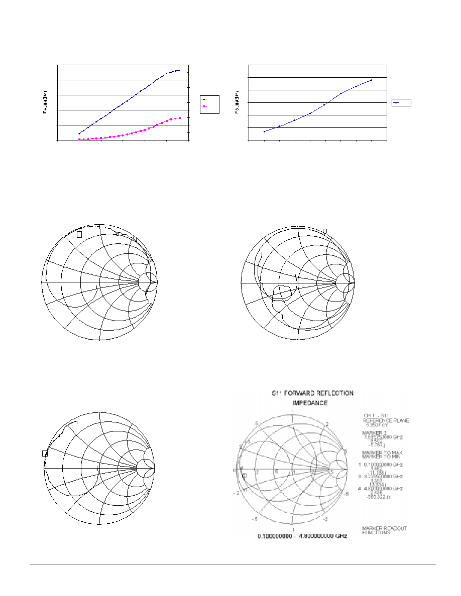
* Pout with CDMA Modulation
Pin = 10 dBm, with CDMA Modulation
Impedance as seen by V
DS1
Impedance as seen by V
DS2
MARKER 2
1.615750000 GHz
MARKER TO MAX
MARKER TO MIN
MARKER READOUT
FUNCTIONS
0
.2
.5
1
2
5
.2
-.2
.5
-.5
1
-1
2
-2
5
-5
0.100000000 -
4.800000000 GHz
S11 FORWARD REFLECTION
IMPEDANCE
CH 1
- S11
REFERENCE PLANE
6.3507 cm
0.100000000 GHz
3.225500000 GHz
4.800000000 GHz
423.067 m
46.696
2.436
2.544
4.971 j
-381.126 jm
18.889 j
31.529 j
1
3
4
1
2
3
4
Impedance as seen by V
DS3
Impedance as seen by V
DS4

4
A
AWT1921S11
Advanced Product information - Rev. 4
Pin 1
Pin 28
Pin 14
Pin 15
GND
V
GS1
/RF
IN
V
D1
V
D2
GND
GND
GND
V
D3
V
D3
V
GS2
V
SS
V
GS3
GND
GND
GND
V
DD
V
REF
V
D4
V
D4
V
D4
V
D4
V
D4
V
D4
V
D4
V
D4
V
GS4
V
GS4
GND
PROCEDURE FOR AMPLIFIER OPERATION AND TEST
1) Slug must be thermally and electrically connected to obtain rated performance
2) The V
SS
Voltage should be applied first to the amplifier prior to V
D1
, V
D2
, V
D3,
or V
D4
voltages
3) V
GS1
, V
GS2
, V
GS3
, V
GS4
may be used as monitor points to verify that the bias circuit is working properly. These
pins should measure as negative voltage potential, after V
SS
is applied.
4) The Bias Pins V
DD
and V
REF
may be applied with no V
SS
voltage present
5) Always Follow ESD precautions when handling these devices
PIN
SIGNAL
DESCRIPTION
1,14,15,28, slug
GND
AC and RF Ground
2
V
GS1
&
RF
IN
First Stage Gate terminal & RF Input
27
V
DD
Positive Supply of Bias Circuit(+5V)
4
V
D2
Second Stage drain supply (+9V)
3
V
D1
First Stage drain supply (+9V)
5,6,7,8
GND
First and Second Stage Source ground
9,10
V
D3
Third Stage drain supply (+9V)
11
V
GS2
Second Stage Gate Terminal
26
V
REF
Bias control Pin (+5V)
12
V
SS
Negative Supply for Bias Circuit (-5V)
13
V
GS3
Third Stage Gate terminal
16,17
V
GS4
Fourth Stage Gate terminal
18-25
V
D4
Fourth Stage drain supply (+9V) & RF out
PIN DESCRIPTION

5
A
AWT1921S11
Advanced Product information - Rev. 4
2
23
28
3
22
7
4
8
20
21
24
25
18
19
10
9
C1
F3
C7
F2
C1
2
C1
4
F5
C1
8
C2
2
C4
V
D4
V
D2
V
D3
V
DD
/V
RE
F
V
SS
GN
D
V
G4
A
W
T
192
1S
11
V
D2
V
D1
RF
IN
/V
GS
1
GN
D
V
RE
F
V
DD
V
G3
V
D4
V
GS2
V
SS
GN
D
V
GS
4
V
D1
RF
IN
5 6
26
R4
13
27
14
15
SLUG
V
D3
C
F1
C5
C1
0
C1
1
C1
3
C3
R3
1
C1
5
C1
6
C1
7
R2
C1
F4
L5
C2
3
R5
17
16
12
11
1610 1626.5 MHZ TEST CIRCUIT SCHEMATIC

6
A
AWT1921S11
Advanced Product information - Rev. 4
DESIGNATION
VALUE
C1,C3,C5,C22
2.2
�
F
C2,C7,C9,C24
Not Used
C4
15 pF
C6, C10
10 pF
C11,C19
27
pF
C12,C13,C20,C21
33
pF
C14,C16,C17,C23
0.01
uF
C15
22 pF
C18
4.7
pF
F1,F2,F3,F4,F5
Feritte
L1,L3
Shim
L2
2.7
nH
L4
8 nH
L5
47 nH
R2,
R5
5600
?
R3
1500
?
R4
2200
?
TEST CIRCUIT SCHEMATIC FOR 1610 -1626.5 MHZ APPLICATION
Notes:
1. Material 6 layer FR4
2. 1 oz. copper
3. 14 mil layers
4. Gerber files available
1610 1626.5 MHz Test Circuit Layout

7
A
AWT1921S11
Advanced Product information - Rev. 4
D
T
HEAT SINK
E
S
A
A
2
A
1
h
a
SLUG
LE
C
L
e
Notes:
1. Controlling dimensions : inches
2. Dimension d does not includemold flash, protrusions or
gate burrs. Mold flash, rotrusions and gate burrs shall
not exceed 0.006 (0.16mm)
3. Dimension e does not include inter-lead or protrusions.
Inter-lead flash and protrusions shall not exceed
4. 0.010 (0.25mm) per side.
5. Maximum lead twist/skew to be 0.002 (0.05mm)
5. Mold flash shall not extend more than 0.010 (0.25mm)
on any edge of heat slug
PACKAGE OUTLINE
INCHES
MILLIMETERS
SYMBOL
MIN.
MAX.
MIN.
MAX.
NOTE
A
0.087
0.093
2.21
2.36
A
1
0.000
0.004
0.00
0.10
A
2
0.087
0.089
2.21
2.25
B
0.008
0.012
0.36
0.46
C
0.007
0.009
0.18
0.25
D
0.400
0.408
10.16
10.36
2
E
0.292
0.296
7.42
7.52
2
e
0.025
BSC
0.64
BSC
4
H
0.410
0.418
10.41
40.62
h
0.018
0.024
0.48
0.61
L
0.034
0.038
0.86
0.97
LE
0.84
1.37
a
0
8
0
8
S
0.139
0.141
3.54
3.55
5
T
0.349
0.351
8.86
8.92
5

8
ANADIGICS, Inc.
35 Technology Drive
Warren, New Jersey 07059
Tel: (908) 668-5000 / Fax: (908) 668-5132
Email: Mkg@anadigics.com
www.anadigics.com
IMPORTANT NOTICE
ANADIGICS, Inc. reserves the right to make changes to its products or discontinue any product at any time without notice. The Advanced Product data
sheets and product specifications contained in this data sheet are subject to change prior to a products formal introduction. The information in this data
sheet has been carefully checked and is assumed to be reliable. However, ANADIGICS assumes no responsibility for inaccuracies. ANADIGICS strongly
urges customers to verify that the information they are using is current before placing orders.
WARNING
ANADIGICS products are not intended for use in life support appliances, device, or systems. Use of an ANADIGICS product in any such application
without written consent is prohibited.
A
AWT1921S11
Advanced Product information - Rev. 4
Designation
Value
Manufacture
Manufacture Part #
Web Address
C1,C3,C5,C22
2.2
�
F
Panasonic
ECS-H1AY225R
www.panasonic.com
C2,C7,C9,C24
Not Used
C4
15 pF
Murata
GRM36COG150J50
www.murata.com
C6,C10
10 pF
Murata
GRM36COG100J50
C11,C19
27 pF
Murata
GRM36COG270J50
www.murata.com
C12,C13,C20,C21
33 pF
Murata
GRM36COG330J50
www.murata.com
C14,C16,C17, C23
0.01 uF
Murata
GRM36X7R103K16
www.murata.com
C15
22 pF
Murata
GRM36COG220J50
www.murata.com
C18
4.7 pF
American Technical Ceramics
ATC100A4R7CW150X
www.atc-cap.com
F1,F2,F3,F4,F5
Ferrite 47
@ 100 MHz, 1A Rating
Taiyo Yuden
BK2125HS470
www.t-yuden.com
L1, L3
Shim
L2
2.7 nH
Toko
LL2012-F2N7S
www.tokoam.com
L4
8 nH
Coilcraft
A03T
www.coilcraft.com
L5
47 nH
Coilcraft
0805CS470XMBC
www.coilcraft.com
R2,R5
5600
Panasonic
ERJ-36SYJ562V
www.panasonic.com
R3
1500
W
Panasonic
ERJ-36SYJ302V
www.panasonic.com
R4
2200
W
Panasonic
ERJ-36SYJ512V
www.panasonic.com