01/2006
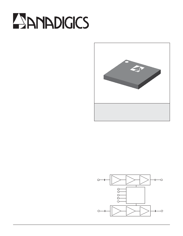
Figure 1: Block Diagram
FEATURES
∑
Internal Reference Voltage
∑
Integrated Power Control Scheme
∑
InGaP HBT Technology
∑
ESD Protection on All Pins (2.5 kV)
∑
Low profile 1.3 mm
∑
Small Package Outline 7 mm x 7 mm
∑
EGPRS Capable (class 12)
∑
RoHS Compliant Package, 250
o
C MSL-3
GMSK MODE
∑
Integrated power control (CMOS)
∑
+35.5 dBm GSM850/900 Output Power
∑
+33.5 dBm DCS/PCS Output Power
∑
55 % GSM850/900 PAE
∑
53 % DCS/PCS PAE
∑
Power control range > 50 dB
EDGE MODE
∑
+29 dBm GSM850/900 Output Power
∑
+28.5 dBm DCS/PCS Output Power
∑
25 % GSM850/900 PAE
∑
30 % DCS/PCS PAE
∑
64 dB Typical ACPR (400 kHz)
∑
74 dB Typical ACPR (600 kHz)
APPLICATIONS
∑
Dual/Tri/Quad Band Handsets and PDAs
∑
Dual/Tri/Quad Band Wireless Data Cards
PRODUCT DESCRIPTION
This power amplifier module supports dual, tri and
quad band applications for GMSK and 8-PSK modu-
lation schemes using an open loop polar architec-
ture. There are two amplifier chains, one to support
GSM850/900 bands, the other for DCS/PCS bands.
Each amplification chain is optimized for excellent
EDGE efficiency, power, and linearity in a Polar loop
environment while maintaining high efficiency in the
GSM/GPRS mode.
The module includes an internal reference voltage
and integrated power control scheme for use in both
GMSK and 8-PSK operation. This facilitates fast and
easy production calibration and reduces the num-
ber of external components required to complete a
power control function.
AWT6168R
Quad-band GSM/GPRS/Polar EDGE
Power Amplifier Module
with Integrated Power Control
PRELIMINARY DATA SHEET - REV 1.0
GSM850/900_IN
T
X
_EN
DCS/PCS_IN
GSM850/900_OUT
GSM850/900
Bias/Power
Control
DCS/PCS_OUT
DCS/PCS
BS
V
RAMP
V
BATT
C
EXT
M11 Package
18 Pin 7 mm x 7 mm x 1.3 mm
Surface Mount Module
AWT6168R
The amplifier's power control range is typically 55
dB, with the output power set by applying an analog
voltage to V
RAMP
. All of the RF ports for this device are
internally matched to 50
.
3
AWT6168R
PRELIMINARY DATA SHEET - Rev 1.0
01/2006
Stresses in excess of the absolute ratings may cause
permanent damage. Functional operation is not implied under
these conditions. Exposure to absolute ratings for extended
periods of time may adversely affect reliability.
ELECTRICAL CHARACTERISTICS
Table 2: Absolute Maximum Ratings
R
E
T
E
M
A
R
A
P
N
I
M
X
A
M
S
T
I
N
U
(
e
g
a
tl
o
V
y
l
p
p
u
S
V
T
T
A
B
)
-
7
+
V
(
r
e
w
o
P
t
u
p
n
I
F
R
F
R
N
I
)
-
1
1
m
B
d
(
e
g
a
tl
o
V
l
o
r
t
n
o
C
V
P
M
A
R
)
3
.
0
-
8
.
1
V
(
e
r
u
t
a
r
e
p
m
e
T
e
g
a
r
o
t
S
T
G
T
S
)
5
5
-
0
5
1
C
∞
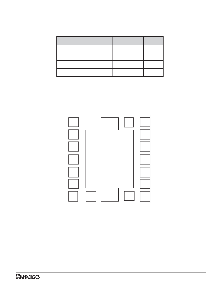
18
1
9
8
7
2
3
4
5
6
10
16
11
13
15
12
14
17
GND
V
CC2
>+2500 V
<-2500 V
V
CC2
>+2500 V
<-2500 V
GND
GND
GND
GND
GND
V
OUT
>+2500 V <-2500 V
GSM_OUT
>+2500 V <-2500 V
DCS/PCS_OUT
>+2500 V <-2500 V
GSM_IN
>+1500 V <-1500 V
DCS/PCS_IN
>+2500 V <-2500 V
BS
>+2500 V <-2500 V
TX_EN
>+2500 V <-2500 V
V
BATT
>+2500 V <-2500 V
C
EXT
>+2500 V <-2500 V
V
RAMP
>+2500 V <-2500 V
GND
Figure 3: ESD Pin Rating
ELECTROSTATIC DISCHARGE SENSITIVITY
The AWT6168R part was tested to determine the
ESD sensitivity of each package pin with respect to
ground. All the package pins were subjected to an
ESD pulse event using the Human Body Model out-
lined in JESD22-A114C.01 in either polarity with re-
spect to ground. The pre and post test I-V character-
istics of each pin are recorded. The ratings on each
pin require that it sustain the ESD event and show
no degradation.

4
AWT6168R
PRELIMINARY DATA SHEET - Rev 1.0
01/2006
Table 5: Digital Inputs
Table 6: Logic Control Table
R
E
T
E
M
A
R
A
P
L
O
B
M
Y
S
N
I
M
P
Y
T
X
A
M
S
T
I
N
U
e
g
a
tl
o
V
h
g
i
H
c
i
g
o
L
V
H
I
2
.
1
-
0
.
3
V
e
g
a
tl
o
V
w
o
L
c
i
g
o
L
V
L
I
-
-
5
.
0
V
t
n
e
r
r
u
C
h
g
i
H
c
i
g
o
L
I|
IH
|
-
-
0
3
mA
t
n
e
r
r
u
C
w
o
L
c
i
g
o
L
I|
IL
|
-
-
0
3
mA
E
D
O
M
L
A
N
O
I
T
A
R
E
P
O
S
B
N
E
_
X
T
0
0
9
/
0
5
8
M
S
G
W
O
L
H
G
I
H
S
C
P
/
S
C
D
H
G
I
H
H
G
I
H
D
E
L
B
A
S
I
D
A
P
-
W
O
L
Table 4: Operating Conditions
The device may be operated safely over these conditions; however, parametric performance is guaranteed
only over the conditions defined in the electrical specifications.
R
E
T
E
M
A
R
A
P
N
I
M
P
Y
T
X
A
M
S
T
I
N
U
S
T
N
E
M
M
O
C
(
e
r
u
t
a
r
e
p
m
e
t
e
s
a
C
T
C
)
0
2
-
-
5
8
C
∞
(
e
g
a
tl
o
v
y
l
p
p
u
S
V
T
T
A
B
)
0
.
3
5
.
3
8
.
4
V
t
n
e
r
r
u
c
e
g
a
k
a
e
l
y
l
p
p
u
s
r
e
w
o
P
-
1
0
1
µ
A
V
T
T
A
B
V
,
V
8
.
4
=
P
M
A
R
,
V
0
=
W
O
L
=
N
E
_
X
T
d
e
il
p
p
a
F
R
o
N
e
g
n
a
R
e
g
a
tl
o
V
l
o
r
t
n
o
C
2
.
0
-
6
.
1
V
(
e
m
i
T
n
o
n
r
u
T
T
N
O
)
-
-
1
µ
s
V
P
M
A
R
W
O
L
=
N
E
_
X
T
,
V
2
.
0
=
Y
H
G
I
H
P
N
I
B
d
5
=
(
e
m
i
T
ff
O
n
r
u
T
T
F
F
O
)
-
-
1
µ
s
V
P
M
A
R
H
G
I
H
=
N
E
_
X
T
,
V
2
.
0
=
Y
W
O
L
P
N
I
B
d
5
=
(
e
m
i
T
e
s
i
R
T
E
S
I
R
)
-
-
1
µ
s
P
T
U
O
m
B
d
0
1
-
=
Y
P
X
A
M
)
B
d
2
.
0
n
i
h
ti
w
(
(
e
m
i
T
ll
a
F
T
L
L
A
F
)
-
-
1
µ
s
P
T
U
O
P
=
X
A
M
Y
)
B
d
2
.
0
n
i
h
ti
w
(
m
B
d
0
1
-
V
P
M
A
R
e
c
n
a
ti
c
a
p
a
C
t
u
p
n
I
-
3
-
F
p
V
P
M
A
R
t
n
e
r
r
u
C
t
u
p
n
I
-
-
0
1
µ
A
e
l
c
y
C
y
t
u
D
-
-
0
5
%

5
AWT6168R
PRELIMINARY DATA SHEET - Rev 1.0
01/2006
Table 7: Electrical Characteristics for GSM850 GMSK mode
Unless otherwise specified: V
BATT
= 3.5 V, P
IN
= 3.0 dBm, Pulse Width =1154
µµ
µµ
µ
s, Duty = 25%,
Z
IN
= Z
OUT
= 50
, T
C
= 25 ∞C, V
RAMP
= 1.6 V, BS = LOW, TX_EN = HIGH
R
E
T
E
M
A
R
A
P
N
I
M
P
Y
T
X
A
M
T
I
N
U
S
T
N
E
M
M
O
C
y
c
n
e
u
q
e
r
F
g
n
it
a
r
e
p
O
(
F
N
I
)
4
2
8
-
9
4
8
z
H
M
P
(
r
e
w
o
P
t
u
p
n
I
N
I
)
0
3
5
m
B
d
P
(
r
e
w
o
P
t
u
p
t
u
O
X
A
M
)
5
.
4
3
8
.
5
3
-
m
B
d
z
H
M
9
4
8
o
t
4
2
8
=
q
e
r
F
r
e
w
o
P
t
u
p
t
u
O
d
e
d
a
r
g
e
D
P
(
T
U
O
)
8
.
2
3
8
.
3
3
-
m
B
d
V
T
T
A
B
T
,
V
0
.
3
=
C
C
∞
5
8
=
P
N
I
m
B
d
0
=
P
@
E
A
P
X
A
M
8
4
3
5
-
%
z
H
M
9
4
8
o
t
4
2
8
=
q
e
r
F
1
n
o
it
a
l
o
s
I
d
r
a
w
r
o
F
-
6
3
-
0
3
-
m
B
d
P
,
V
0
=
N
E
_
X
T
N
I
m
B
d
5
=
2
n
o
it
a
l
o
s
I
d
r
a
w
r
o
F
-
0
3
-
0
2
-
m
B
d
V
,
H
G
I
H
=
N
E
_
X
T
P
M
A
R
V
2
.
0
=
P
N
I
m
B
d
5
=
n
o
it
a
l
o
s
I
s
s
o
r
C
F
2
(
o
F
3
,
o
)
t
r
o
p
S
C
P
/
S
C
D
@
-
7
2
-
0
2
-
m
B
d
P
T
U
O
<
m
B
d
5
.
4
3
c
i
n
o
m
r
a
H
d
n
o
c
e
S
-
0
2
-
0
1
-
m
B
d
P
T
U
O
<
m
B
d
5
.
4
3
c
i
n
o
m
r
a
H
d
r
i
h
T
-
0
4
-
5
1
-
m
B
d
P
T
U
O
<
m
B
d
5
.
4
3
n
(
o
f
*
n
>
F
,
)
4
o
5
7
.
2
1
z
H
G
-
0
3
-
0
1
-
m
B
d
P
T
U
O
<
m
B
d
5
.
4
3
y
ti
li
b
a
t
S
P
,
s
e
s
a
h
P
ll
A
1
:
8
=
R
W
S
V
T
U
O
<
m
B
d
5
.
4
3
-
-
6
3
-
m
B
d
F
T
U
O
z
H
G
1
<
-
-
0
3
-
m
B
d
F
T
U
O
z
H
G
1
>
s
s
e
n
d
e
g
g
u
R
n
o
it
a
d
a
r
g
e
D
t
n
e
n
a
m
r
e
P
o
N
s
e
l
g
n
A
e
s
a
h
P
ll
A
,
1
:
0
1
R
W
S
V
P
T
U
O
<
m
B
d
5
.
4
3
r
e
w
o
P
e
s
i
o
N
X
R
-
4
8
-
2
8
-
m
B
d
F
X
T
,
z
H
k
0
0
1
=
W
B
R
,
z
H
M
9
4
8
=
F
X
R
P
,
z
H
M
4
9
8
o
t
9
6
8
=
T
U
O
<
m
B
d
5
.
4
3
s
s
o
L
n
r
u
t
e
R
t
u
p
n
I
-
1
:
5
.
1
1
:
5
.
2
R
W
S
V
P
T
U
O
<
m
B
d
5
.
4
3