 | –≠–ª–µ–∫—Ç—Ä–æ–Ω–Ω—ã–π –∫–æ–º–ø–æ–Ω–µ–Ω—Ç: AAT3141 | –°–∫–∞—á–∞—Ç—å:  PDF PDF  ZIP ZIP |

AAT3141
High Efficiency 1X/1.5X/2X Charge Pump
for White LED Applications
3141.2005.12.1.2
1
ChargePump
TM
General Description
The AAT3141 is a low noise, constant frequency
charge pump DC/DC converter that uses a tri-mode
load switch (1X), fractional (1.5X), and doubling (2X)
conversion to maximize efficiency for white LED appli-
cations. The device produces current levels up to
30mA on each of its four current source outputs to
drive various arrangements of LEDs from a 2.7V to
5.5V input. Outputs may be operated individually or in
parallel for driving higher-current LEDs. A low external
parts count (two 1µF flying capacitors and two small
1µF capacitors at V
IN
and CP) make the AAT3141 ide-
ally suited for small battery-powered applications.
The AAT3141 is equipped with AnalogicTech's unique
AutoBiasTM technology which allows individual LEDs
to be powered either by charge pump or battery input,
determined internally and automatically to maximize
the power efficiency even with a large difference in
LED forward voltage.
AnalogicTech's Advanced Simple Serial ControlTM
(AS
2
CwireTM) digital input is used to enable, disable,
and set the LED drive current with a 32-level logarith-
mic scale LED brightness control. The AAT3141 has a
thermal management system to protect the device in
the event of a short-circuit condition at an output pin.
Built-in soft-start circuitry prevents excessive inrush
current during start-up. A high charge pump switching
frequency enables the use of very small external
capacitors. In shutdown mode, the device disconnects
the load from V
IN
and reduces quiescent current to
less than 1µA. The AAT3141 is available in the very
small, Pb-free 12-pin TSOPJW package.
Features
∑
V
IN
Range: 2.7V to 5.5V
∑
Tri-Mode 1X, 1.5X, and 2X Charge Pump for
Maximum Efficiency and V
F
Coverage
∑
Drives Low-V
F
and High-V
F
Type LEDs
∑
Up to Four 30mA Outputs
∑
AS
2
Cwire Independent 3+1 Output Addressing
∑
32-Position Logarithmic Scale with Digital
Control
∑
Low Noise Constant Frequency Operation
∑
1MHz Switching Frequency
∑
AutoBias Technology
∑
Small Application Circuit
∑
Regulated Output Current
∑
Automatic Soft Start
∑
No Inductors
∑
I
Q
<1µA in Shutdown
∑
12-Pin TSOPJW Package
Applications
∑
Color (RGB) Lighting
∑
Programmable Current Sources
∑
White LED Backlighting
∑
White Photo Flash for Digital Still Cameras
Typical Application
C
IN
1
µF
V
BATTERY
C
CP
1
µF
EN/SET
C1
1
µF
C2
1
µF
D3
D2
D1
VIN
CP
C1+
C1-
C2+
C2-
D1
D2
D3
D4
EN/SET
GND
AAT3141
D4

AAT3141
High Efficiency 1X/1.5X/2X Charge Pump
for White LED Applications
2
3141.2005.12.1.2
Pin Descriptions
Pin Configuration
TSOPJW-12
(Top View)
1
2
3
4
5
6
12
11
10
9
8
7
C2+
CP
C1-
C1+
D3
D2
C2-
GND
IN
EN/SET
D1
D4
Pin #
Symbol
Function
1
C2+
Flying capacitor 2 positive terminal. Connect a 1µF capacitor between C2+
and C2-.
2
CP
Charge pump output. Requires 1µF capacitor connected between this pin and
ground.
3
C1-
Flying capacitor 1 negative terminal.
4
C1+
Flying capacitor 1 positive terminal. Connect a 1µF capacitor between C1+
and C1-.
5
D3
Current source output #3.
6
D2
Current source output #2.
7
D4
Current source output #4.
8
D1
Current source output #1.
9
EN/SET
AS
2
Cwire serial interface control pin.
10
IN
Input power supply. Requires 1µF capacitor connected between this pin and
ground.
11
GND
Ground.
12
C2-
Flying capacitor 2 negative terminal.

AAT3141
High Efficiency 1X/1.5X/2X Charge Pump
for White LED Applications
3141.2005.12.1.2
3
Absolute Maximum Ratings
1
Thermal Information
3
Symbol
Description
Value
Units
P
D
Maximum Power Dissipation
4
625
mW
JA
Maximum Thermal Resistance
160
∞C/W
Symbol
Description
Value
Units
V
IN
Input Voltage
-0.3 to 6
V
V
EN/SET
EN/SET to GND Voltage
-0.3 to V
IN
+ 0.3
V
I
OUT
2
Maximum DC Output Current
150
mA
T
J
Operating Junction Temperature Range
-40 to 150
∞C
1. Stresses above those listed in Absolute Maximum Ratings may cause permanent damage to the device. Functional operation at condi-
tions other than the operating conditions specified is not implied. Only one Absolute Maximum Rating should be applied at any one time.
2. Based on long-term current density limitation.
3. Mounted on an FR4 board.
4. Derate 6.25mW/∞C above 25∞C.

AAT3141
High Efficiency 1X/1.5X/2X Charge Pump
for White LED Applications
4
3141.2005.12.1.2
Electrical Characteristics
1
C
IN
= C
CP
= C
1
= C
2
= 1.0µF; T
A
= -40∞C to +85∞C, unless otherwise noted. Typical values are at T
A
= 25∞C,
V
IN
= 3.5V.
Symbol
Description
Conditions
Min Typ Max Units
Input Power Supply
V
IN
Operation Range
2.7
5.5
V
I
cc
Operating Current
VD1:D4 = 2.0V, CP = 1X
550
µA
No Load Current, CP = 1.5X
3
5
mA
I
SHDN
Shutdown Current
V
IN
= 3.5V, EN/SET = 0
1
µA
I
DX
Output Current Accuracy
2
V
IN
= 3.5V, T
A
= 25∞C
-10
10
%
V
IN
= 3.5V, T
A
= 25∞C, Code 28 17.1
19
20
mA
I
(D-Match)
Current Matching
3
VD1:D4 = 3.6V, V
IN
= 3.5V
-3
±0.5
3
%
CP
Charge Pump Section Efficiency
V
IN
= 3.5V, I
OUT(TOTAL)
= 120mA,
93
%
Measured from IN to CP
Charge Pump Section
T
SS
Soft-Start Time
50
µs
F
CLK
Clock Frequency
1
MHz
EN/SET
V
EN(L)
Enable Threshold Low
V
IN
= 2.7V
0.4
V
V
EN(H)
Enable Threshold High
V
IN
= 5.5V
1.4
V
T
EN/SET LO
EN/SET Low Time
0.3
75
µs
T
EN/SET HI MIN
Minimum EN/SET High Time
50
ns
T
EN/SET HI MAX
Maximum EN/SET High Time
75
µs
T
OFF
EN/SET Off Timeout
500
µs
T
LAT
EN/SET Latch Timeout
500
µs
I
EN/SET
EN/SET Input Leakage
V
EN/SET
= 5.5V, V
IN
= 5.5V
-1
1
µA
1. The AAT3141 is guaranteed to meet performance specifications over the -40∞C to +85∞C operating temperature range and is assured
by design, characterization, and correlation with statistical process controls.
2. Codes 2 through 7 are guaranteed to be within
±
15% of stated current level.
3. Current matching is defined as I
(D-Match)
= (I
D
- I
AVE
)/I
AVE
.
AAT3141
High Efficiency 1X/1.5X/2X Charge Pump
for White LED Applications
3141.2005.12.1.2
5
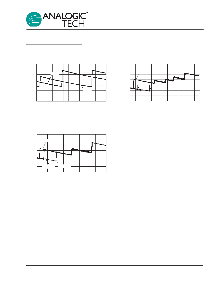
Typical Characteristics
Unless otherwise noted, V
IN
= 3.5V, C
IN
= C
CP
= C
1
= C
2
= 1µF, T
A
= 25∞C.
Input Voltage (V)
Efficiency (%)
30
40
50
60
70
80
90
100
2.9
3.0
3.1
3.2
3.3
3.4
3.5
3.6
3.7
3.8
3.9
4.0
4.1
4.2
Code 32
Code 28
Code 26
Efficiency vs. Input Voltage
(D1-D2 = 3.5V; D3-D4 = 3.2V)
Efficiency vs. Input Voltage
(D1 = 3.5V; D2 = 3.3V; D3 = 3.2V; D4 = 3.0V)
Input Voltage (V)
Efficiency (%)
30
40
50
60
70
80
90
100
2.9
3.0
3.1
3.2
3.3
3.4
3.5
3.6
3.7
3.8
3.9
4.0
4.1
4.2
Code 32
Code 28
Code 26
Input Voltage (V)
Efficiency (%)
30
40
50
60
70
80
90
100
2.9
3.0
3.1
3.2
3.3
3.4
3.5
3.6
3.7
3.8
3.9
4.0
4.1
4.2
Efficiency vs. Input Voltage
(Code 26)
3.5V
F
3.0V
F