 | –≠–ª–µ–∫—Ç—Ä–æ–Ω–Ω—ã–π –∫–æ–º–ø–æ–Ω–µ–Ω—Ç: DBS2050A | –°–∫–∞—á–∞—Ç—å:  PDF PDF  ZIP ZIP |
2.4 GS/s Dual-Channel
Arbitrary Waveform Generator
C Size VXI Instrument Module
DBS 2050A
Features
Sampling Rate: 2.4 GS/s (Single
Channel)
Bandwidth: 800 MHz Typical
Waveform Resolution: 8 Bit
Voltage Range: 4.0V peak-to-peak
Voltage Offset: ±3.5 VDC
Waveform Memory: 8 Mbytes
Sequence Memory: 4k Segments
100% Performance Tested and
Regulatory Certified
Application Development:
∑ VXI Plug and Play Compliant
Drivers for WIN and Solaris
Frameworks
Applications
Automatic Test Equipment
Telecommunications
Mass Storage
RADAR
Ultrasonics
Navigation
LAN/WAN
Wireless
RF Controls
bus
Introduction
Building on thirty years of success developing state-of-the-art measurement
solutions, Analogic introduces the most advanced broadband stimulus
instrumentation available today.
Engineers and scientists who rely on ultra-high-performance arbitrary waveform
generators can anticipate significant performance improvements from the new
DBS 2050A.
Finally, an arbitrary waveform generator (AWG) possesses the power and flexi-
bility to provide the right signals for your applications.
Dramatically improve the quality of performance characterization testing on
all kinds of electronic devices
Generate arbitrary waveforms, including Pulse Pattern and Sinusoidal stimu-
lus, over a frequency range of DC to 1.2 GHz with 8 bits of vertical resolution
and over 60 dB of programmable gain and offset
Synchronize dual outputs with a maximum time skew of ±100 ps
Produce rise/fall times of 400 ps
Play back waveforms with sample rate jitter of less than 10 ps RMS
Increase memory efficiency by over 100 times over conventional AWG de-
signs by using the flexible waveform and sequence memory architecture
Use waveform independent runtime parameters to change the output level
and offset "on the fly"
Preload up to 4096 unique waveforms in memory and seamlessly link them
for playback (creating very long waveform playback periods), using Dynamic
Waveform Sequencing
Advance from one waveform to the next using conditional waveform repeat
(loop) counts as well as internal or external trigger events.
Generate precise standard waveforms: square, sine, positive and negative
ramps, pulse, noise, triangle, positive and negative haversines, sin(x)/x, and DC
Bring your next high-speed analog or mixed signal design to market faster while
dramatically reducing errors or oversight in critical design verifications. The
DBS 2050A is ideal for use on the production floor or in the laboratory.
General Description
Analog signal outputs are available in true differential or single-ended form for
one channel operation and single ended when operating in dual channel mode.
Output amplitudes are 1.0V peak-to-peak using the primary X1 amplifiers; 4.0V
peak-to-peak using the high-level X4 amplifiers. Offsets can be set to ±3.5V
with 2 mV resolution.
In addition to the full bandwidth output, the DBS 2050A has three selectable low
pass output filters with cutoff frequencies of 200 MHz, 20 MHz and 2 MHz.
Other filter requirements are accommodated with available SMA feed-thru filter
modules.
The sampling clock is built around a precision phase detector capable of
synchronizing to internal or external references. The sample clock rate is
programmable over a range of 600 S/s to 2.4 GS/s. The external reference
input can range from 2.5 MHz to 100 MHz.
Flexible Operating Modes
Each output channel has two physical ports; A and B. This
highly flexible architecture facilitates fast switching
between ports without external control elements.
The high-level output amplifiers are capable of operation to
4.0V peak-to-peak. The low-level output amplifiers deliver
1.0V peak-to-peak waveforms with great spectral purity.
Gain control has 60 dB of adjustment range.
Single Channel Modes
Dynamic Waveform Sequencing
The unique architecture of the DBS 2050A provides a level
of flexibility and functionality not found in any other arbi-
trary waveform generator.
Control of the output signal path is decoupled from wave-
form memory so gain and offset changes can be made
over a wide dynamic range without disruption of the output
signal.
Dual Channel Modes
VXI Bus Interface
The DBS 2050A comes equipped with a fully compliant
VXI Plug and Play Driver, soft front panel and application
source code. The toolset supports application-specific
developments in Visual C/C++ or Visual BASIC, as well as
National Instruments' LabWindows/CVI and LabVIEW.
Waveform creation and editing software is provided by
WavesmithTM, a versatile waveform development system for
Windows. This tool provides a "no programming required"
work environment for rapid prototyping of user waveforms,
as well as direct control of all instrument functions.
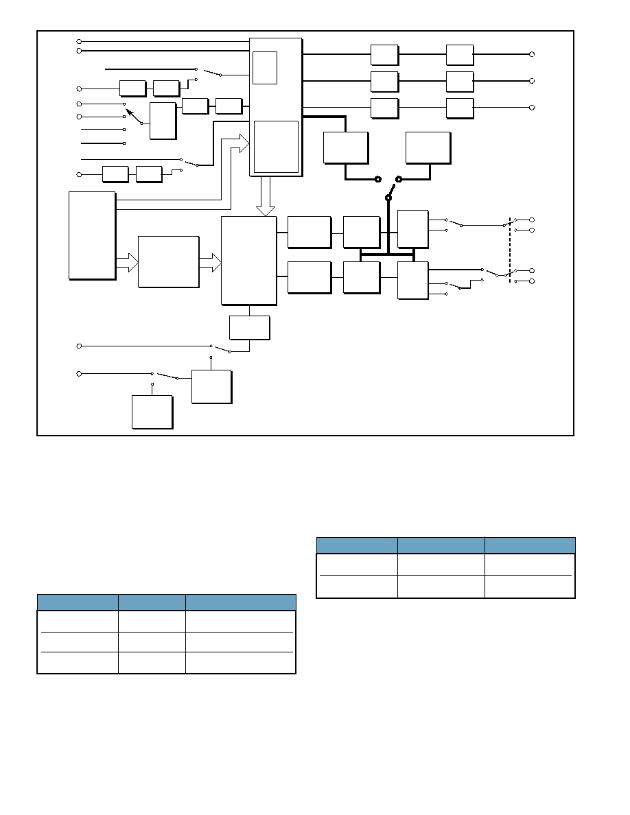
Branch
Vector
Branch SW Commands
Polarity
Level
Polarity
Level
Trigger
Mode
VXI_ECL0
VXI_ECL1
Trigger A
Trigger B
Branch
Trigger
Advance SW Commands
Polarity
Level
Advance
Trigger
VXI Bus
Interface
Waveform
Memory
DACs/Combiner
Internal
Reference
Clock
Ext Clock
Input
Ext Ref
Clock
Input
Sequencer
Branch
Vector
Table
Marker 1
Marker 2
Marker 3
Delay
Delay
Delay
Pulse
Width
Pulse
Width
Pulse
Width
Sequence
Gain/Offset
Direct Gain
and Offset
Low Pass
or
Pass Through
Low Pass
or
Pass Through
Amplitude
Amplitude
Offset
Offset
4X+
1X+
4X+
1X+
1X≠
Output 1A
Output 1B
Output 2A
Output 2B
Sequence
Memory
Time Base
Generator
Phase Lock
Loop
Ch1
Ch2
Programmable
Programmable
Figure 1. DBS 2050A Functional Block Diagram.
Mode
Main Output
Complementary Output
2.0 V Differential
1A
2A
1B
2B
1.0V Single Ended
1A
--
(X1 Output)
1B
--
4.0V Single Ended
1A
--
(X4 Output)
1B
--
Mode
Channel 1 Output
Channel 2 Output
1.0V Single Ended
1A
2A
(X1 Output)
1B
2B
4.0V Single Ended
1A
2A
(X4 Output)
1B
2B
DBS 2050A
Specifications
OUTPUT CHARACTERISTICS
Parameter
Conditions
Value
X1 OUTPUT MODE
Max. Amplitude
Differential
2.0V pk-pk
Single-Ended
1.0V pk-pk
Accuracy
50
Terminated
±2.0% at full scale
Gain Ctrl Accuracy
25∞ ±5∞C
±1% of setting, ±.00025 V/V
Resolution
>3500 steps/60 dB
Flatness (1)
Sinusoid 0.5V pk-pk
±0.5 dB to 30 MHz
±2.0 dB to 300 MHz
Bandwidth
<0.5V pk-pk
>700 MHz
Rise/Fall Time
<0.5V pk-pk
<500 ps
<1.0V pk-pk
<600 ps
Amplitude Con-
50 ns to within 10% of final
trol Settling Time
200 ns to within 20% of final
X4 OUTPUT MODE
Max. Amplitude
Single-Ended Only
4.0V p-p
Accuracy
50
Terminated
±2.0% at full scale
Gain Ctrl Accuracy
25∞ ±5∞C
±1% of setting, ±.00025 V/V
Flatness (1)
Sinusoid 2.0V pk-pk
±0.5 dB to 30 MHz
±2.0 dB to 100 MHz
Bandwidth
<2.0V pk-pk
>165.0 MHz
Rise/Fall Time
<2.0V pk-pk
<2.2 ns
<4.0V pk-pk
<2.5 ns
DC OFFSET
Resolution
2.0 mV
Range
Differential
±2.0V
Single-Ended Mode
±3.5V
Accuracy Single-
±2.0% of setting
Ended Output
Output Mode (X1)
±20 mV
±2.0% of setting
Output Mode (X4)
±80 mV
Accuracy
Common Mode
±2.0% of setting
Differential
X1 Output Mode
±20 mV
Output
Differential
±2.0% of setting
X1 Output Mode
±30 mV
Offset Control
6 µs to within 2%
Settling Time
of new setting Max.
FILTER CHARACTERISTICS
Parameter
Conditions
Value
Type
3-pole Bessel Low Pass
≠3 dB
2 MHz
Bandwidth
Selectable
20 MHz
200 MHz
Rise Time
0.35/Bandwidth
TIME BASE/SAMPLING CLOCK
Parameter
Conditions
Value
INTERNAL SAMPLE CLOCK
Range
Single Channel Mode
600 S/s to 2.4 GS/s
Dual Channel Mode
300 S/s to 1.2 GS/s
Resolution
0.4% of Desired Rate Max.
Accuracy
±2 ppm Typ.
Jitter
100 ns Measurement
<10 ps RMS
Window Internal
Clock Only
EXTERNAL REFERENCE CLOCK INPUT
Range
0.8 ≠ 1.5V pk-pk
2.5 MHz to 100 MHz
Resolution
at
2.5 MHz Steps
Duty Cycle
10 MHz
50% Nom.
Impedance
50 ohms AC coupled
EXTERNAL SAMPLE CLOCK
Range
0.8 ≠ 1.5V pk-pk
100 kHz to 2.4 GHz
Slew Rate 0.5V/ns
TRIGGER CHARACTERISTICS
Parameter
Conditions
Value
MAIN TRIGGER
Sources
Trigger A, Trigger B, ECL0, ECL1
Modes
Free Run, Start, Stop, Gate and Start/Stop
Threshold
±10.0V
Range
Threshold
±5% of Setting
Accuracy
±140 mV Typ.
Hysteresis
40 mV pk-pk
Input Impedance
4.0 k
Nom.
Trigger to
Dual Channel
42 ns + 17 clock
Output
Mode
cycles
Delay
Single Channel
42 ns + 35 clock
Mode
cycles
BRANCH AND ADVANCE TRIGGER
Threshold
TTL Mode
1.5V Typ.
Zero Crossing
0V Typ.
Input Impedance
10 k
Nom.
Trigger to Output
1.66 µs + 256/FS (2)
Delay
SINEWAVE CHARACTERISTICS
Parameter
Conditions
Value
X1 OUTPUT MODE
SFDR
<10 MHz
Measured from 1 MHz
>45 dBc
<50 MHz
to Nyquist.
>40 dBc
<200 MHz
1.0V pk-pk 2.4 GS/s
>30 dBc
SINAD
50 MHz Carrier
1.0V pk-pk 2.4 GS/s
>37 dBc
5 MHz to Nyquist
X4 OUTPUT MODE
SFDR
Measured from 1 MHz
<50 MHz
to 600 MHz
>40 dBc
4.0V pk-pk
0V Offset
SINAD
50 MHz Carrier
4.0V pk-pk
37 dBc
5 MHz to
605 MHz BW
MARKER OUTPUTS 1, 2, 3
Parameter
Conditions
Value
Output
No Load
TTL
Impedance
50
Nom.
Delay Range
0 to 2 x 10⁶ x sample
clock period Max.
Delay Resolution
32 x sample clock period
Pulse Width
0 to 1.31 x 10⁵ x sample
Range
clock period Max.
Resolution
32 x sample clock period
Response
PHYSICAL CHARACTERISTICS
Parameter
Conditions
Value
Weight
Without Packaging
7.25 kg
Size
VXI Double Wide C Size
Cooling
7 liters/sec
REGULATORY
VXI Compliance
VXI Plug and Play Register based instrument
REV 1.4
Electromagnetic
EN61326-1 Class A
Compatibility
FCC Part 15, Subpart B, Class A
Safety
EN61010-1, IEC 1010-1, UL3111-1
DBS 2050A
Specifications (cont.)
Analogic Corporation
Test & Measurement Division
8 Centennial Drive
Peabody, MA 01960-7987, USA
Tel: (978) 977-3000
Fax: (978) 977-6814
email: t&m_info@analogic.com
www.analogic.com
Printed in U.S.A.
© 2000/2001 ANALOGIC Corporation
Bulletin No. 16-100649 REV 0 8/00 2M
CALIBRATION/WARRANTY
Maintenance
Unit is self-calibrating at startup
Warm-Up Time
15 minutes
Recommended
Annually
Factory
Re-Certification
ACCESSORIES
User's Manual
Support Software
Includes:
∑ VXI P&P Driver for WIN NT, WIN 95, WIN 98
∑ LabView Soft Front Panel Source Code
∑ WavesmithTM Waveform Development
Software for Win NT, 95, 98
Contact Analogic for a complete listing of other VXI products and accessories.
ENVIRONMENTAL
Parameter
Conditions
Value
Operating
At Rated Air Flow
Temperature
Full Compliance
10∞C to 40∞C
Range
with Specifications
Storage
Temperature
≠20∞C to +70∞C
Range
Relative
Non-Condensing
10%≠90%
Humidity
Total Power
Operating
130 watts
Dissipation
DC Current
+5 VDC
6.2A
Consumption
≠5.2 VDC
8.5A
+24 VDC
0.1A
≠24 VDC
0.1A
+12 VDC
0.7A
≠12 VDC
1.0A
≠2 VDC
3.6A
Vibration
Operating
IEC 68-2-6
Non-Operating
Shock
Operating
6.0G, 11 ms _sine
IEC 68-2-29
Non-Operating
10G
Notes
All specifications are subject to change without notice.
All specifications are valid within the operating limits stated.
Calibration values are not user accessible.
All specifications are valid for 50
output terminations unless otherwise stated.
1. Allowance Made for sin(x)/x Rolloff.
2. FS -- sample clock rate.
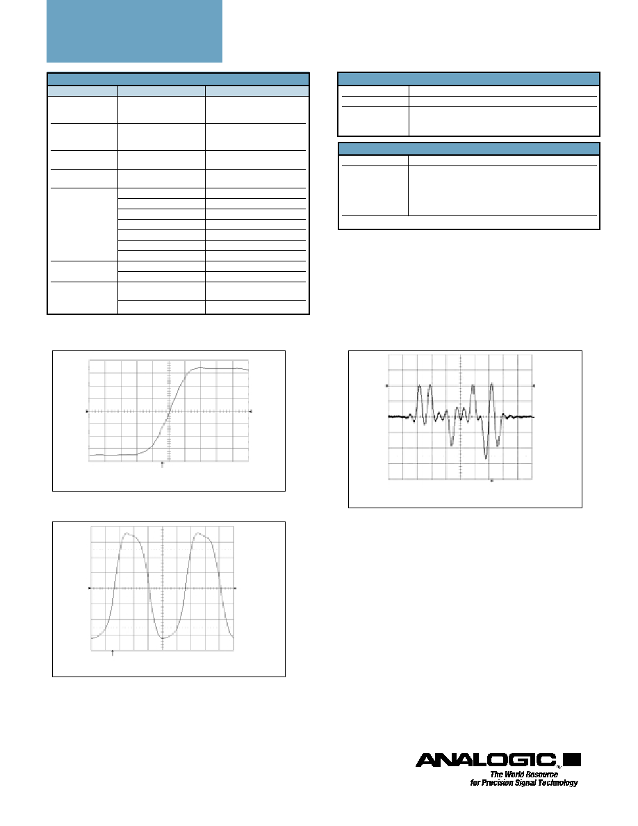
Typical rise time ≠FS to +FS in one sample clock period.
Square wave, 6 pts/cycle. Sampled at 2.4 GS/s.
Typical PR4 pulse pattern. 6 ns step size. 10 pts/bit pulse.
140 mV
140 mV
8 GS/s
.5 ns
Rise (2)
Over+ (2)
429 ps
1.57%
25 GS/s
.2 ns
2
100 mV
8 GS/s
20 ns
2
2