 | –≠–ª–µ–∫—Ç—Ä–æ–Ω–Ω—ã–π –∫–æ–º–ø–æ–Ω–µ–Ω—Ç: DBS2055 | –°–∫–∞—á–∞—Ç—å:  PDF PDF  ZIP ZIP |
Introduction
Building on thirty years of success developing state-of-the-art measurement so-
lutions, Analogic introduces the DBS2055 -- a powerful adaptation of our most
advanced broadband stimulus instrument, the DBS2050A.
Engineers and scientists who rely on ultra-high-performance arbitrary waveform
generators can anticipate significant performance improvements from this new
instrument. The DBS2055 can:
Generate arbitrary waveforms, including Pulse Pattern and Sinusoidal stimu-
lus, over a frequency range of DC to 2 GHz with up to 8 bits of vertical resolu-
tion and over 60 dB of programmable gain and offset
Produce rise/fall times of < 250 ps
Play back waveforms with sample rate jitter of < 10 ps RMS
Increase memory efficiency by > 100 times over conventional AWG designs
by using the flexible waveform and sequence memory architecture
Use waveform-independent runtime parameters to change the output level
and offset "on the fly"
Preload up to 4,096 unique waveforms in memory and seamlessly link them
for playback (creating very long waveform playback periods), using Dynamic
Waveform Sequencing
Advance from one waveform to the next using conditional waveform repeat
(loop) counts as well as internal or external trigger events
Synchronize the analog outputs with up to 6 independent TTL level markers
Generate precise standard waveforms: square, sine, positive and negative
ramps, pulse, noise, triangle, positive and negative haversines, sin(x)/x, and DC
Bring your next high-speed analog or mixed signal design to market faster while
dramatically reducing errors or oversights in critical design verifications. The
DBS2055 is ideal for use on the production floor or in the laboratory.
General Description
The DBS2055 has three modes of operation: single channel, synchronous dual
channel, and synchronous quad channel.
In single channel mode the unit operates at the highest sample rate, 4.8 GS/s,
using the internal time base. Single channel mode produces the fastest edges
and covers the widest bandwidth. Dual synchronous mode takes advantage of
the DBS2055's unique architecture to produce matched waveforms with negligi-
ble time skew and jitter of <10 ps RMS. Quad channel mode extends this capa-
bility to four waveforms with an individual sample rate of 1.2 GS/s. In single or
dual sync modes the unit produces true differential or single ended waveforms
with full scale output levels up to 4.0V peak to peak.
continued
Features
Sampling Rate: 4.8 GS/s
Bandwidth: 1.9 GHz
Waveform Resolution: 8-Bit
Voltage Range: 4.0V peak-to-peak
in X4 Output Mode
Voltage Offset: ±3.5 VDC
Waveform Memory: 8 Mbytes
Sequence Memory: 4k Segments
100% Performance Tested with
NIST Traceable Cert. of Comp.
Application Development: VXI Plug
and Play Compliant Drivers for
Win 98, NT, 2K
IEEE-488/1394/100Base-T Ethernet
Applications
Automatic Test Equipment
HDD Read/Write Chan. Development
Telecom/Datacom
Mass Storage
RADAR
Ultrasonics
Navigation
LAN/WAN
Wireless
RF Controls
Fiber
4.8 GS/s Universal, High Speed
Arbitrary Waveform Generator
DBS2055
Preliminar
y
7/1/02
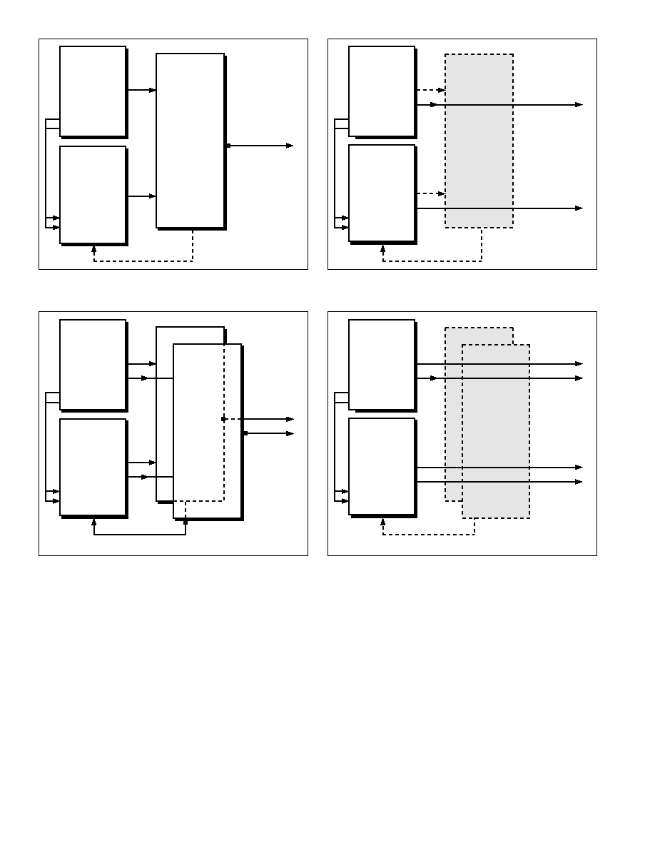
Master Module
DBS2055 Output
Combiner 1
Sync Clk+
Sync Clk≠
Output 1A
+
IN1
IN2
CAL
Sync Clk+
Sync Clk≠
Slave Module
Output 1A
REF Clk IN
Out
Master Module
Channel 1 Output
Combiner 1
Sync Clk+
Sync Clk≠
Output 1B
+
Channel 2 Output
+
Sync Clk+
Sync Clk≠
Slave Module
Output 1A
REF Clk IN
Output 1A
Output 1B
Master Module
Channel 1 Output
+
Combiner 1
Combiner 2
Output 1B
Sync Clk+
Sync Clk≠
Output 2B
≠
Channel 2 Output
+
≠
Sync Clk+
Sync Clk≠
Slave Module
Output 1B
REF Clk IN
Output 2B
Master Module
DBS2055 Output
Combiner 1
Output 1A
Sync Clk+
Sync Clk≠
Sync Clk+
Sync Clk≠
Slave Module
IN 1
≠
+
Output 1A
IN 2
IN 1
IN 2
Combiner 2
Cal
Cal
IN 2
IN 1
REF Clk IN
Output 2A
Output 2A
DBS2055 Single Channel Mode (Single Ended Output)
DBS2055 Single Channel Mode (Differential Output)
DBS2055 Dual Synchronous Mode (Single Ended Outputs)
DBS2055 Dual Synchronous Mode (Differential Outputs)
Continued from page 1
The provided waveform pre-compensation algorithms can
be used to exchange output level for dramatic increases in
analog bandwidth. The operator defines the desired signal
bandwidth and the waveforms conform to the desired fre-
quency response. The DBS2055 also achieves stunning
frequency response over the full bandwidth of operation.
Amplitude flatness is less than ±0.5 dB up to 700 MHz.
Waveform pre-compensation involves the application of
principles from sampling theory that compensates for the
frequency response of the system, including cables.
Waveform creation and editing software is provided by
WavesmithTM, a versatile waveform development system
for Windows. This tool provides a "no programming re-
quired" work environment for rapid prototyping of user
waveforms, as well as di
rect control of all instrument
functions.
HDD-NARB, Hard Disk Drive Read/Write
Channel Testing
HDD/NARB is an application specific software tool that,
when combined with the DBS2055, tackles one of the
toughest problems faced by developers in the hard disk
drive industry: managing the rapid advances in Read/Write
channel complexity, data rates and sensitivity. An HDD-
NARB and DBS2055 can literally replace the physical
media head.
HDD-NARB generates accurate and precise pulse pat-
terns representative of actual drive media, waveforms that
are critical to design verification by both chip and disk
drive manufacturers. HDD-NARB will easily model media
noise, thermal asperities, and dropouts ≠ the three deadly
effects that plague disk drives.
SINEWAVE CHARACTERISTICS
Parameter
Conditions
Value
X1 OUTPUT MODE
SFDR
<10 MHz
Measured from 1 MHz
>45 dBc
<50 MHz
to Nyquist.
>40 dBc
<200 MHz
1.0 Vp-p 4.8 GS/s
>30 dBc
SINAD
50 MHz Carrier
1.0 Vp-p 4.8 GS/s
>37 dBc
5 MHz to Nyquist
X4 OUTPUT MODE
SFDR
Measured from 1 MHz
<50 MHz
to 600 MHz
>40 dBc
4.0 Vp-p
0V Offset
SINAD
50 MHz Carrier
4.0 Vp-p
37 dBc
5 MHz to
605 MHz BW
FILTER CHARACTERISTICS
Parameter
Conditions
Value
Type
3-pole Bessel Low Pass
≠3 dB
2 MHz
Bandwidth
Selectable
20 MHz
200 MHz
Rise Time
0.35/Bandwidth
TIME BASE/SAMPLING CLOCK
Parameter
Conditions
Value
INTERNAL SAMPLE CLOCK
Range
Single Channel Mode
2410 MS/s to 4.8 GS/s
Dual Channel Mode
600 S/s to 2.4 GS/s
Quad Channel Mode
300 S/s to 1.2 GS/s
Resolution
0.4% of Desired Rate Max.
Accuracy
±2 ppm Typ.
Jitter
100 ns Measurement
<10 ps RMS
Window Internal
Clock Only
EXTERNAL REFERENCE CLOCK INPUT
Range
0.8 ≠ 1.5 Vp-p
2.5 MHz to 100 MHz
Resolution
at
2.5 MHz Steps
Duty Cycle
10 MHz
50% Nom.
Impedance
50 ohms AC coupled
EXTERNAL SAMPLE CLOCK
Range
0.8 ≠ 1.5 Vp-p Slew
100 kHz to 2.4 GHz
Rate 0.5V/ns Applied to
Master, 50
AC Coupled
TRIGGER CHARACTERISTICS
Parameter
Conditions
Value
MAIN TRIGGER
Sources
Trigger A, Trigger B
Modes
Free Run, Start, Stop, Gate and Start/Stop
Threshold
±10.0V
Range
Threshold
±5% of Setting
Accuracy
±140 mV Typ.
Hysteresis
40 mVp-pk
Input Impedance
4.0 k
Nom.
Trigger to
Quad Channel
42 ns + 17
Output
Mode
clock cycles
Delay
Dual Synchronous
42 ns + 35
Mode
clock cycles
Single Channel
42 ns + 70
Mode
clock cycles
BRANCH AND ADVANCE TRIGGER
(Multi-Channel Mode)
Threshold
TTL Mode
1.5V Typ.
Zero Crossing
0V Typ.
Input Impedance
10 k
Nom.
Trigger to Output
1.66 µs + 256/FS (2)
Delay
MARKER OUTPUTS 1, 2, 3
Parameter
Conditions
Value
Output
No Load
TTL
Impedance
50
Nom.
Delay Range
Single Channel
0 to 4 x 10⁶ x sample
clock period Max.
Delay Resolution
Single Channel
64 x sample clock period
Pulse Width
0 to 2.62 x 10⁵ x sample
Range
clock period Max.
Resolution
64 x sample clock period
Response
OUTPUT CHARACTERISTICS
Parameter
Conditions
Value
X1 OUTPUT MODE
Max. Amplitude
Differential
2.0 Vp-p
Single-Ended
1.0 Vp-p
Accuracy
50
Terminated
±2.0% at full scale
Gain Ctrl Accuracy
25∞ ±5∞C
±1% of setting, ±.00025 V/V
Resolution
>3500 steps/60 dB
Flatness (3)
0.5 Vp-p, 4.8 GS/s
±0.2 dB
<30 MHz
0.5 Vp-p, 4.8 GS/s
±0.3 dB
<300 MHz
0.5 Vp-p, 4.8 GS/s
±0.5 dB
<700 MHz
Bandwidth
<0.1 Vp-p
1.9 GHz
(Small Signal)
4.8 GS/s
Rise/Fall Time (3)
0.1 Vp-p, 4.8 GS/s
<250 ps
Amplitude Con-
50 ns to within 10% of final
trol Settling Time
200 ns to within 20% of final
X4 OUTPUT MODE
Max. Amplitude
Single-Ended Only
4.0 Vp-p
Accuracy
50
Terminated
±2.0% at full scale
Gain Ctrl Accuracy
25∞ ±5∞C
±1% of setting, ±.00025 V/V
Flatness (1)
Sinusoid 2.0 Vp-p
±0.5 dB to 30 MHz
±2.0 dB to 100 MHz
Bandwidth
<2.0 Vp-p
>165.0 MHz
Rise/Fall Time
<2.0 Vp-p
<2.2 ns
<4.0 Vp-p
<2.5 ns
DC OFFSET
Resolution
2.0 mV
Range
Differential
±2.0V
Single-Ended Mode
±3.5V
Accuracy Single-
Output Mode (X1)
±2.0% of setting
Ended Output
±20 mV
Output Mode (X4)
±2.0% of setting
±80 mV
Accuracy
Common Mode
±2.0% of setting
Differential
X1 Output Mode
±20 mV
Output
Differential
±2.0% of setting
X1 Output Mode
±30 mV
Offset Control
6 µs to within 2%
Settling Time
of new setting Max.
DBS2055
Specifications
Printed in U.S.A.
© 2001, 2002 ANALOGIC Corporation
Bulletin No. 16-100676 REV 1 5/02
Analogic Corporation
Test & Measurement Division
8 Centennial Drive
Peabody, MA 01960-7987, USA
Tel: (978) 977-3000
Fax: (978) 977-6814
email: t&m_info@analogic.com
www.analogic.com
DBS2055
Specifications, Cont.
REGULATORY
VXI Compliance
VXI Plug and Play Register based instrument
Electromagnetic
EN61326-1 Class A
Compatibility
FCC Part 15, Subpart B, Class A
Safety
EN61010-1, CSA C22.2 No. 1010.1, UL61010A-1
ENVIRONMENTAL
Parameter
Conditions
Value
Operating
At Rated Air Flow
Temperature
Full Compliance
10∞C to 40∞C
Range
with Specifications
Storage
Temperature
≠20∞C to +70∞C
Range
Relative
Non-Condensing
10%≠90%
Humidity
Total Power
Operating
260 watts
Dissipation
DC Current
+5 VDC
12.4 A Max.
Consumption
≠5.2 VDC
17 A Max.
+24 VDC
0.2 A Max.
≠24 VDC
0.2 A Max.
+12 VDC
1.4 A Max.
≠12 VDC
2.0 A Max.
≠2 VDC
7.2 A Max.
Vibration
Operating
IEC 68-2-6
Non-Operating
IEC 68-2-6
Shock
Operating
6.0G, 11 ms _sine
IEC 68-2-29
Non-Operating
10G
Transportation
ISTA Project 2A
CALIBRATION/WARRANTY
Warm-Up Time
15 minutes
Recommended
Annually
Factory
Re-Certification
ACCESSORIES
User's Manual
Support Software
Includes:
∑ VXI P&P Driver for Framework, 98,2K, Win NT
∑ LabWindows CVI Soft Front Panel Source Code
∑ WavesmithTM Waveform Development
Software for Win NT, 98, 2K
∑ HDD-NARB Pulse Pattern and Synthesis Software for
Hard Disk Drive Industry
Contact Analogic for a complete listing of other VXI products and accessories.
Notes
All specifications are subject to change without notice.
All specifications are valid within the operating limits stated.
Calibration values are not user accessible.
All specifications are valid for 50
output terminations unless otherwise stated.
1. Allowance made for sin(x)/x Rolloff.
2. Fs ≠ sample clock rate.
3. With Waveform Pre-Compensation
PHYSICAL CHARACTERISTICS
Parameter
Conditions
Value
Weight
Without Packaging
16 kg
Size
VXI 4-Slot Wide C Size
Cooling
4 liters min/sec/slot
@ 0.5 mm H20
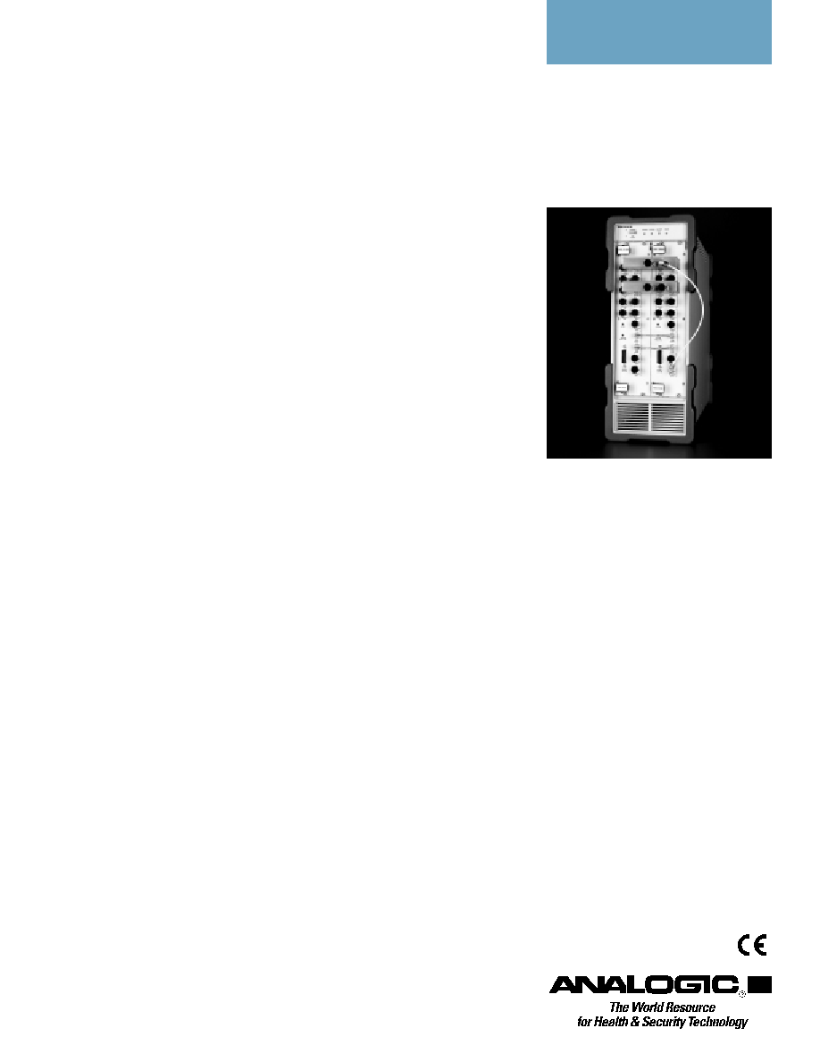
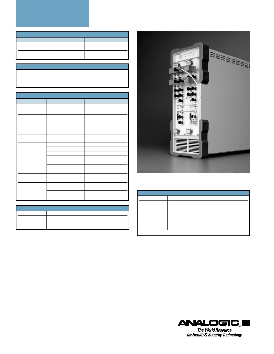
Shown Installed in Analogic DP7040-2 Bench Top Chassis.