 | –≠–ª–µ–∫—Ç—Ä–æ–Ω–Ω—ã–π –∫–æ–º–ø–æ–Ω–µ–Ω—Ç: AAT1101 | –°–∫–∞—á–∞—Ç—å:  PDF PDF  ZIP ZIP |
Advanced Analog Technology, Inc.
≠
≠
≠
Advanced Analog Technology, Inc
.
≠
Page 1 of 23 V 1.0
AAT1101 Series
Details are subject to change without notice
TRIPLE OUTPUT TFT LCD PWM CONTROLLER
Features
Complete PWM Power Control Circuitry
Precision Reference: 1.25V±1% (25
C
o
)
Low Operating Voltage: 2.5V to 6.5V
Under-Voltage Lockout Protection
5V or 3.3V Selectable Over Voltage
Lockout Protection (AAT1101/A only)
AAT1101/AAT1101A/AAT1101C: 500kHz Fixed
AAT1101B: 50k~1MHz Programmable
Internal Power Up Sequence Control
Totem Pole Output
Output Short Circuit Protection
Low Dissipation Current: 2.5mA
(f=500kHz, Duty=50%)
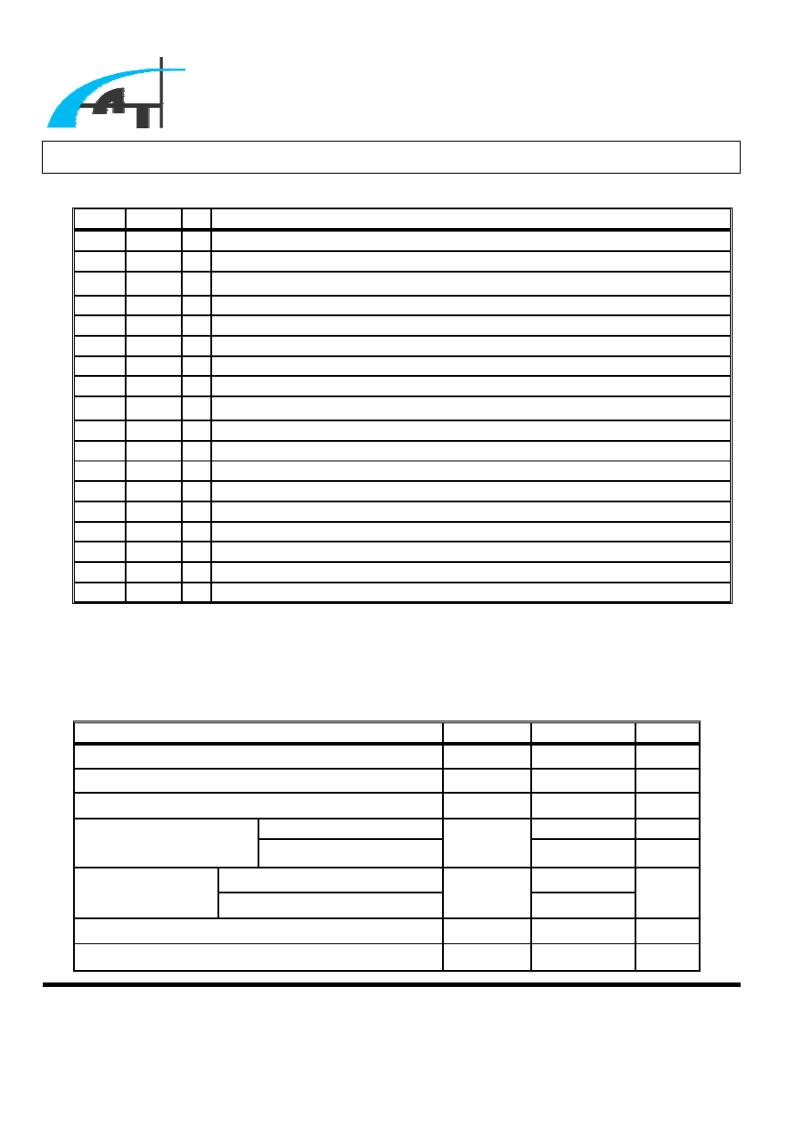
Pin Configuration
TOP VIEW
1
2
3
4
5
6
7
8
16
15
14
13
12
11
10
9
IE2
PRDB
OUT2
OUT3
OUT1
SCP
GND
SHDN
IE1
IE3
EO 1
PRDS
CHC
OVS (OSC) (NC)
DD
V
REF
V
(TSSOP-16 PACKAGE)
General Description
The AAT1101 series provide an integrated
triple-channel pulse width modulation (PWM) solution
for the power supply of LCD displays. These devices
offer system engineers the flexibility to tailor-make the
power supply circuitry for specific applications. Each
channel contains its own error amplifier, PWM
comparator, dead≠time control (DTC) and output driver.
The under-voltage protection, over voltage protection,
power sequence control, shutdown control circuit,
oscillator, short circuit protection, and voltage reference
circuits are the common features of the three channels.
The AAT1101 series contain two exclusive boost
circuits at CH1, CH3 and an exclusive buck_boost
circuit at CH2. AAT1101's Power Up sequence initiates
at CH1 then CH2 and finally CH3. AAT1101A/C's
Power Up sequence acts in the order of CH2, CH3, and
then CH1. AAT1101B's Power Up sequence starts
from CH2, CH1, and then CH3. At the completion of
the Power Up sequencing, the SCP pin stays low and
enters the Wait State of short circuit protection. Power
Up sequencing delay and short circuit protection delay
are set by connecting a capacitor to the SCP pin.
Furthermore, these devices can operate with supply
voltage ranging from 2.5V to 6.5V and function
efficiently in an environment with low power supply.
With a minimum number of external components, the
AAT1101 series offer a simple and cost effective
solution for TFT LCD.
Advanced Analog Technology, Inc.
≠
≠
≠
Advanced Analog Technology, Inc
.
≠
Page 2 of 23 V 1.0
AAT1101 Series
Pin Description
Pin # Name I/O
Description
1
IE2
I Inverted Input of Error Amplifier 2 (EA2)
2
PRDB O Power Ready Output
3
DD
V
I Supply Voltage
4
OUT2 O Channel 2 (CH2) Output
5
OUT3 O Channel 3 (CH3) Output
6
OUT1 O Channel 1 (CH1) Output
7 GND
Ground
8
SCP
I Short Circuit Protection
9
REF
V
O Reference Voltage Output
10*
OVS I/O 3.3V or 5.0V Over Voltage Selection and Over Voltage Output
10** OSC I/O Frequency Setting Capacitor & Resistor Input
10*** NC
NC
11
CHC O Channel Control
12
PRDS I Power Ready Set
13
EO1 I/O Feedback Input of Error Amplifier 1 (EA1)
14
IE1
I Inverted Input of Error Amplifier 1 (EA1)
15
IE3
I Inverted Input of Error Amplifier 3 (EA3)
16
SHDN I Shutdown Control
*
AAT1101A only
**AAT1101B only
***AAT1101C only
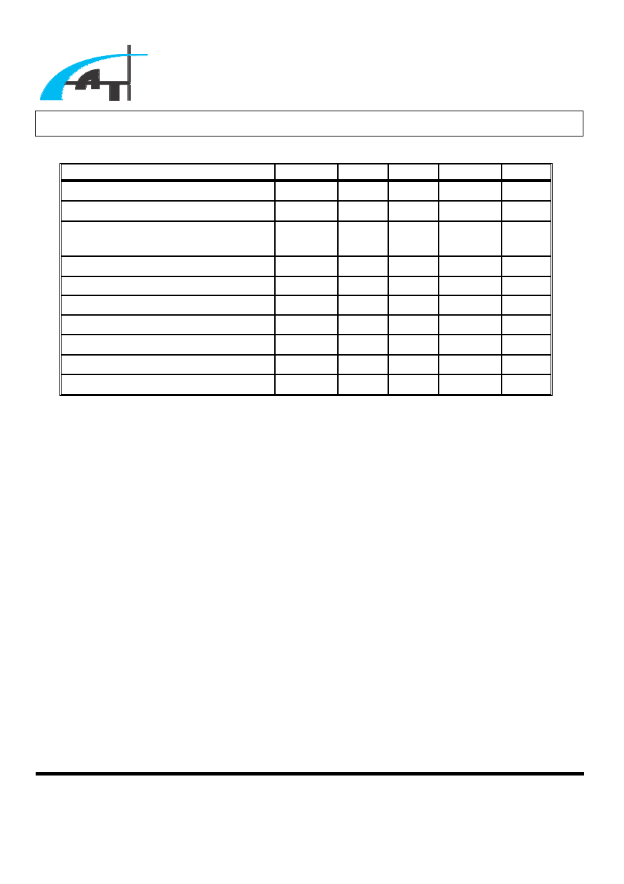
Absolute Maximum Ratings
CHARACTERISTICS SYMBOL
VALUE
UNIT
Supply Voltage
DD
V
8 V
Input Voltage (
-
IE
)
I
V
DD
V
V
Output Voltage
O
V
DD
V +0.3
V
CH1, CH3
41
-
/+21 mA
Output Current
CH2
O
I
21
-
/+41
mA
Sink (
w
t 2
s
µ
, Duty10%)
+200
Output Peak Current Source (
w
t 2
s
µ
, Duty10%)
opeak
I
200
-
mA
Operating Free-Air Temperature Range
C
T
20
-
to +85
o
C
Storage Temperature Range
storage
T
45
-
to +125
o
C
Advanced Analog Technology, Inc.
≠
≠
≠
Advanced Analog Technology, Inc
.
≠
Page 3 of 23 V 1.0
AAT1101 Series
Recommended Operating Conditions
Symbol
Min
Typ
Max
Unit
Supply Voltage,
DD
V
(with
OVS
R
)
DD
V
2.5 5.0 5.7 V
Supply Voltage,
DD
V
(without
OVS
R
)
DD
V
2.5 3.3 3.8 V
Supply Voltage,
DD
V
(AAT1101B/C Only
DD
V
2.5 3.3 6.5 V
Input Voltage, IE1, IE3
13
I
V
0.95 - 1.55 V
Input Voltage, IE2
2
I
V
0.4 - 1.0 V
Output Voltage
O
V
0
-
DD
V
V
Output Current,
1
out
I
,
3
out
I
13
O
I
- -
40
-
/+20
mA
Output Current,
2
out
I
2
O
I
- -
20
-
/+40
mA
Output Current of Error Amplifier
OE
I
- - 60 µA
Operating Free-Air Temperature
C
T
20
-
- 85
o
C
Advanced Analog Technology, Inc.
≠
≠
≠
Advanced Analog Technology, Inc
.
≠
Page 4 of 23 V 1.0
AAT1101 Series
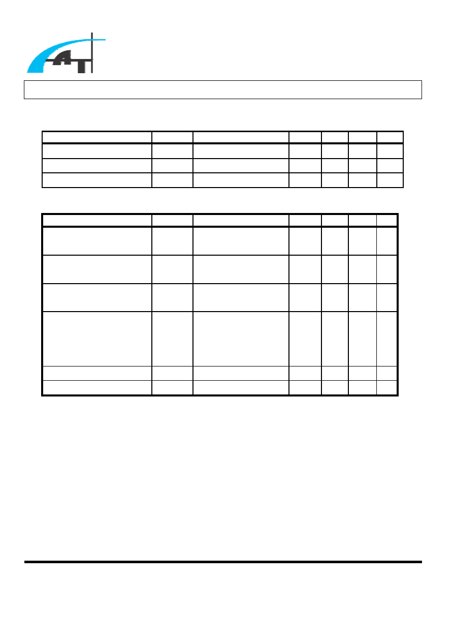
Electrical Characteristics,
DD
V
= 3.3V (Unless Otherwise Specified) (See Note 1)
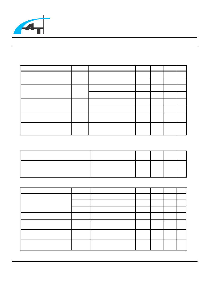
OscillatorAAT1101/AAT1101A/AAT1101C
OscillatorAAT1101B only
Parameter
Test Condition
Min Typ Max
Unit
Frequency
OSC
f
OSC
C
= 130pf,
OSC
R
= 7
k
400 500 600
kHz
"H" Level Output Voltage
OSCH
V
OSC
C
= 130pf,
OSC
R
= 7
k
0.95 1.00 1.05 V
"L" Level Output Voltage
OSCL
V
OSC
C
= 130pf,
OSC
R
= 7
k
0.35 0.40 0.45 V
Frequency Change with
DD
V
V
f
DD
V = 2.5V to 6.5V,
C
T = 25
o
C
OSC
C
= 130pf,
OSC
R
= 7
k
- 1 2
%
Frequency Changes with
C
T
T
f
-
- 5
10
%
Output Source Current
OSC
I
-
220
-
200
-
180
-
A
µ
Parameter
Test Condition
Min Typ Max Unit
Frequency
OSC
f
C
T = 25
o
C
400 500 600 kHz
Frequency Changes with
C
T
T
f
- 5
10
%
Maximum Duty Cycle
xon
T
70 85 95 %
Advanced Analog Technology, Inc.
≠
≠
≠
Advanced Analog Technology, Inc
.
≠
Page 5 of 23 V 1.0
AAT1101 Series
Electrical Characteristics,
DD
V
= 3.3V (Unless Otherwise Specified) (Cont.)
Under Voltage (UV) and Over Voltage (OV) Protection
Parameter
Test
Condition
Min
Typ
Max
Unit
C
T
= 25
o
C, AAT1101/A/B
2.1 2.3 2.5 V
UV Upper Threshold
Voltage
UPH
V
C
T
= 25
o
C, AAT1101C
2.0 2.2 2.4 V
C
T
= 25
o
C, AAT1101/A/B
1.9 2.1 2.3 V
UV Lower Threshold
Voltage
UPL
V
C
T
= 25
o
C, AAT1101C
1.7 1.87 2.05 V
C
T
= 25
o
C, AAT1101/A/B
0.1 0.2 0.3 V
UV Hysteresis (
UPH
V
≠
UPL
V
)
HYS
V
C
T
= 25
o
C, AAT1101C
0.18 0.33 0.48 V
OV 3.3V Threshold
Voltage**
33
OP
V
C
T
= 25
o
C
3.8 4.1 4.4 V
OV 5V Threshold
Voltage**
5
OP
V
C
T
= 25
o
C, OVS connects a
56
k
resistor to
DD
V
5.7 6.1 6.5 V
**: AAT1101/AAT1101A only
Shutdown Control
Parameter
Test Condition
Min
Typ
Max Unit
Shutdown Release Input Voltage
2.0 - - V
Shutdown Enable Input Voltage
- -
0.5
V
Short Circuit Protection Control
Parameter
Test
Condition
Min
Typ
Max
Unit
1
r
V
CH1 (EO1)
1.10 1.15 1.20 V
1
r
V
CH3 (IE3)
1.20 1.25 1.30 V
Input Threshold Voltage
2
r
V
CH2 (IE2)
0.67 0.70 0.73 V
Latch Reset Voltage by
DD
V
VDD
_
R
V
C
T = 25
o
C
0.8 1.5 1.8 V
Latch Reset Voltage by
SHDN
SHDN
_
R
V
C
T = 25
o
C
- -
0.5
V
Short-Circuit Detection
Threshold Voltage
3
r
V
1.20 1.25 1.30 V
SCP Terminal Source
Current
SCP
I
6
.
2
-
0
.
2
-
4
.
1
-
A
µ