 | –≠–ª–µ–∫—Ç—Ä–æ–Ω–Ω—ã–π –∫–æ–º–ø–æ–Ω–µ–Ω—Ç: AAT1123 | –°–∫–∞—á–∞—Ç—å:  PDF PDF  ZIP ZIP |

AAT1123
1MHz Step-Down Converter
1123.2006.05.1.5
1
SwitchReg
TM
General Description
The AAT1123 SwitchRegTM is a member of
AnalogicTech's Total Power Management ICTM
(TPMICTM) product family. It is a 1MHz step-down
converter with an input voltage range of 2.7V to
5.5V and output as low as 0.6V. Its low supply cur-
rent, small size, and high switching frequency
make the AAT1123 the ideal choice for portable
applications.
The AAT1123 is available in either a fixed version
with internal feedback or a programmable version
with external feedback resistors. It can deliver up
to 600mA of load current while maintaining a low
25µA no load quiescent current. The 1MHz switch-
ing frequency minimizes the size of external com-
ponents while keeping switching losses low. The
AAT1123 feedback and control delivers excellent
load regulation and transient response with a small
output inductor and capacitor.
The AAT1123 is designed to maintain high efficien-
cy throughout the operating range and provides
fast turn-on time.
The AAT1123 is available in a space-saving
2.0x2.1mm SC70JW-8 package and is rated over
the -40∞C to +85∞C temperature range.
Features
∑
V
IN
Range: 2.7V to 5.5V
∑
V
OUT
Adjustable Down to 0.6V
-- Fixed or Adjustable Version
∑
Fast Turn-On Time (100µs Typical)
∑
25µA No Load Quiescent Current
∑
Up to 97% Efficiency
∑
Output Current Up to 600mA
∑
1MHz Switching Frequency
∑
Soft Start
∑
Over-Temperature Protection
∑
Current Limit Protection
∑
100% Duty Cycle Low-Dropout Operation
∑
0.1µA Shutdown Current
∑
SC70JW-8 Package
∑
Temperature Range: -40∞C to +85∞C
Applications
∑
Cellular Phones
∑
Digital Cameras
∑
Handheld Instruments
∑
Microprocessor / DSP Core / IO Power
∑
PDAs and Handheld Computers
∑
USB Devices
Typical Application (Fixed Output Voltage)
AAT1123 Efficiency
(V
OUT
= 2.5V; L = 10
H)
Output Current (mA)
Efficiency (%)
60
70
80
90
100
0.1
1
10
100
1000
V
IN
= 3.3V
4.7
H
L1
22
F
C1
4.7
F
C2
EN
1
OUT
2
VIN
3
LX
4
AGND
5
PGND
6
PGND
7
PGND
8
AAT1123
U1
V
IN
V
O
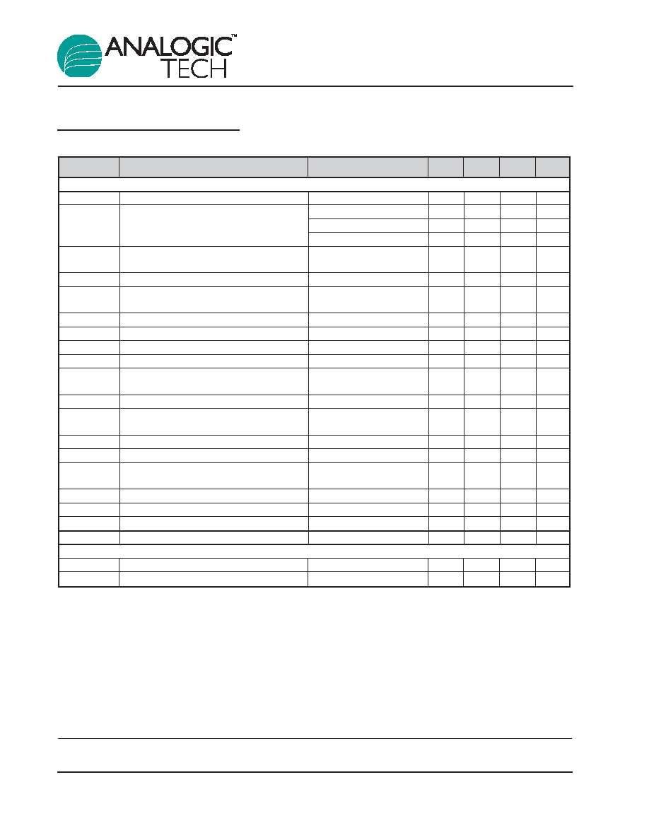
Pin Descriptions
Pin Configuration
SC70JW-8
(Top View)
OUT
VIN
LX
PGND
PGND
PGND
AGND
EN
1
2
3
4
5
6
7
8
Pin #
Symbol
Function
1
EN
Enable pin.
2
OUT
Feedback input pin. This pin is connected either directly to the converter
output or to an external resistive divider for an adjustable output.
3
VIN
Input supply voltage for the converter.
4
LX
Switching node. Connect the inductor to this pin. It is internally connected to
the drain of both high- and low-side MOSFETs.
5
AGND
Non-power signal ground pin.
6, 7, 8
PGND
Main power ground return pin. Connect to the output and input capacitor
return.
AAT1123
1MHz Step-Down Converter
2
1123.2006.05.1.5
Absolute Maximum Ratings
1
Thermal Information
Symbol
Description
Value
Units
P
D
Maximum Power Dissipation (SC70JW-8)
625
mW
JA
Thermal Resistance
2
(SC70JW-8)
160
∞C/W
Symbol
Description
Value
Units
V
IN
Input Voltage GND
6.0
V
V
LX
L
X
to GND
-0.3 to V
P
+ 0.3
V
V
OUT
OUT to GND
-0.3 to V
P
+ 0.3
V
V
EN
EN to GND
-0.3 to 6.0
V
T
J
Operating Junction Temperature Range
-40 to 150
∞C
T
LEAD
Maximum Soldering Temperature (at leads, 10 sec)
300
∞C
AAT1123
1MHz Step-Down Converter
1123.2006.05.1.5
3
1. Stresses above those listed in Absolute Maximum Ratings may cause permanent damage to the device. Functional operation at condi-
tions other than the operating conditions specified is not implied. Only one Absolute Maximum Rating should be applied at any one time.
2. Mounted on an FR4 board.
Electrical Characteristics
1
T
A
= -40∞C to +85∞C, unless otherwise noted. Typical values are T
A
= 25∞C, V
IN
= 3.6V.
Symbol
Description
Conditions
Min
Typ
Max Units
Step-Down Converter
V
IN
Input Voltage
2.7
5.5
V
V
IN
Rising
2.6
V
V
UVLO
UVLO Threshold
Hysteresis
100
mV
V
IN
Falling
1.8
V
V
OUT
Output Voltage Tolerance
I
OUT
= 0 to 600mA,
-3.5
+3.5
%
V
IN
= 2.7V to 5.5V
V
OUT
Output Voltage Range
0.6
V
IN
V
I
Q
Quiescent Current
No Load, 0.6V Adjustable
25
50
µA
Version
I
SHDN
Shutdown Current
EN = AGND = PGND
1.0
µA
I
OUT_X
Maximum Load Current
600
mA
R
DS(ON)H
High Side Switch On Resistance
0.45
R
DS(ON)L
Low Side Switch On Resistance
0.40
I
LXLEAK
LX Leakage Current
V
IN
= 5.5V, V
LX
= 0 to V
IN
,
1
µA
EN = GND
V
Linereg
Line Regulation
V
IN
= 2.7V to 5.5V
0.5
%/V
V
OUT
Out Threshold Voltage Accuracy
0.6V Output, No Load
591
600
609
mV
T
A
= 25∞C
I
OUT
Out Leakage Current
0.6V Output
0.2
µA
R
OUT
Out Impedance
>0.6V Output
250
k
T
S
Start-Up Time
From Enable to Output
100
µs
Regulation
F
OSC
Oscillator Frequency
T
A
= 25∞C
0.7
1.0
1.5
MHz
T
SD
Over-Temperature Shutdown Threshold
140
∞C
T
HYS
Over-Temperature Shutdown Hysteresis
15
∞C
EN
V
EN(L)
Enable Threshold Low
0.6
V
V
EN(H)
Enable Threshold High
1.4
V
I
EN
Input Low Current
V
IN
= V
FB
= 5.5V
-1.0
1.0
µA
AAT1123
1MHz Step-Down Converter
4
1123.2006.05.1.5
1. The AAT1123 is guaranteed to meet performance specifications over the -40∞C to +85∞C operating temperature range and is assured
by design, characterization, and correlation with statistical process controls.

AAT1123
1MHz Step-Down Converter
1123.2006.05.1.5
5
Typical Characteristics
DC Regulation
(V
OUT
= 1.5V; L = 4.7
H)
Output Current (mA)
Output Error (%)
-3.0
-2.0
-1.0
0.0
1.0
2.0
3.0
0.1
1
10
100
1000
V
IN
= 3.6V
V
IN
= 4.2V
V
IN
= 2.7V
Efficiency vs. Load
(V
OUT
= 1.5V; L = 4.7
H)
Output Current (mA)
Efficiency (%)
50
60
70
80
90
100
0.1
1
10
100
1000
V
IN
= 3.6V
V
IN
= 4.2V
V
IN
= 2.7V
DC Regulation
(V
OUT
= 2.5V; L = 10
H)
Output Current (mA)
Output Error (%)
-3.0
-2.0
-1.0
0.0
1.0
2.0
3.0
0.1
1
10
100
1000
V
IN
= 3.6V
V
IN
= 3.3V
V
IN
= 3.0V
Efficiency vs. Load
(V
OUT
= 2.5V; L = 10
H)
Output Current (mA)
Efficiency (%)
60
70
80
90
100
0.1
1
10
100
1000
V
IN
= 3.0V
V
IN
= 3.6V
V
IN
= 3.3V
DC Regulation
(V
OUT
= 3.3V; L = 10
H)
Output Current (mA)
Output Error (%)
-3.0
-2.0
-1.0
0.0
1.0
2.0
3.0
0.1
1
10
100
1000
V
IN
= 4.2V
V
IN
= 3.9V
Efficiency vs. Load
(V
OUT
= 3.3V; L = 10
H)
Output Current (mA)
Efficiency (%)
60
70
80
90
100
0.1
1
10
100
1000
V
IN
= 3.9V
V
IN
= 4.2V